
In the fast-paced world of industrial IoT, the hidden costs of subpar hardware can cripple your margins. While off-the-shelf components might look cheaper initially, the long-term reality is often plagued by maintenance outages and poor signal integrity. Today, we explore how strategic investment in custom-engineered gateway PCB assembly serves as the foundational pillar for reducing your Total Cost of Ownership (TCO) and accelerating deployment cycles.
The Hidden Expense: Why Standard Gateway Hardware Fails at Scale
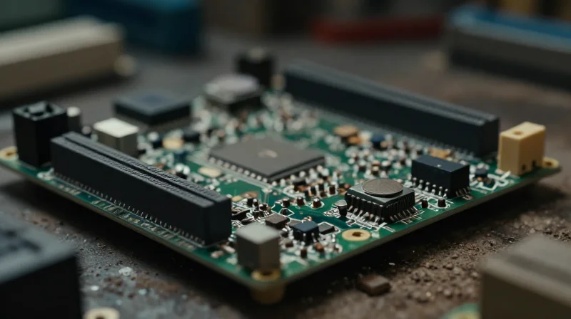
The Fragility of Off-the-Shelf Hardware
Mass-produced gateways are designed for enterprise IT rooms, not the extreme conditions of industrial deployments. While their low initial price point seems attractive, the hidden costs of frequent field failures, diagnostic labor, and network downtime quickly erode any projected ROI, making custom PCB assembly a more fiscally responsible choice for long-term scalability.
Common Failure Points in Harsh Environments
| Component | Standard Hardware Failure | Custom PCB Mitigation |
|---|---|---|
| Connectors | Corrosion and loosening due to vibration | Solder-down or ruggedized locking headers |
| Thermal Management | Passive cooling failure in enclosed boxes | Integrated heat dissipation copper pours |
| Power Input | Voltage spikes cause surge damage | Industrial-grade transient voltage protection |
| Environmental | Condensation on sensitive circuitry | Conformal coating and optimized trace routing |
Key Considerations for Industrial Reliability
- Why do standard connectors fail in industrial settings?
Standard Ethernet and power ports are not vibration-rated; over time, the mechanical stress leads to intermittent contact, resulting in network dropouts that are notoriously difficult to debug remotely. - How does PCB design influence operational longevity?
A custom layout allows for the strategic placement of components to minimize EMI interference and optimize heat paths, ensuring critical chipsets remain within their thermal operating window even in confined, non-ventilated enclosures. - Is custom assembly really cheaper long-term?
Yes. By eliminating unnecessary consumer-grade features—such as integrated web servers or visual indicators that are never used in the field—you reduce the points of failure and streamline the assembly, leading to a lower Total Cost of Ownership (TCO) over a 5-year deployment cycle.
Engineering for Longevity: The Impact of Signal Integrity
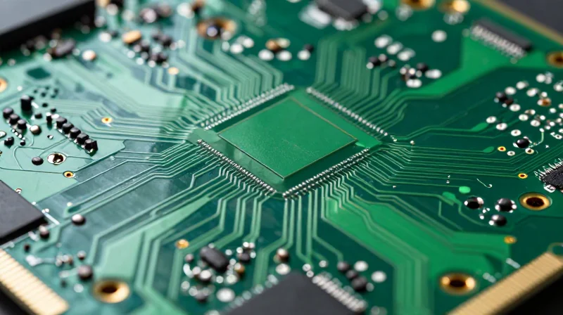
The Correlation Between Signal Integrity and Operational Costs
In industrial LoRaWAN deployments, signal integrity is the primary determinant of network reliability. When PCB layouts are generic or poorly optimized, issues such as impedance mismatch, signal crosstalk, and electromagnetic interference (EMI) manifest as increased bit error rates. For an operator, this translates to intermittent packet loss that requires on-site technician visits to debug—visits that can cost thousands of dollars per incident. By engineering custom PCB assemblies for superior signal routing, we eliminate the root causes of radio frequency (RF) degradation, ensuring consistent data transmission without the need for manual intervention.
Mitigating Failure Points Through Precision Design
| Feature | Generic Gateway Impact | Custom PCB Mitigation |
|---|---|---|
| Impedance Control | Reflections/RF Loss | Zero-Loss Data Path |
| Layer Stackup | Susceptible to EMI | Shielded Signal Integrity |
| Ground Plane | Unstable Reference | Noise-Free Return Path |
Frequently Asked Questions: Engineering for Longevity
- How does PCB layout affect LoRaWAN range?
A well-optimized PCB minimizes insertion loss between the radio transceiver and the antenna connector. This ensures the maximum possible link budget, which maintains connectivity in challenging industrial environments where signals are typically attenuated by metallic obstructions. - Why does custom PCB design lead to higher ROI?
While custom PCB assembly has higher upfront NRE costs, the return on investment is realized through significantly reduced truck rolls, less downtime, and a longer lifecycle of the hardware in extreme temperature or high-vibration conditions. - Can better signal integrity reduce power consumption?
Yes. Optimized signal paths prevent retransmissions caused by corrupted data packets. By reducing the number of retries required to complete a handshake, the gateway consumes less power and experiences less thermal stress on its components.
Custom PCB Manufacturing vs. Off-the-Shelf: A TCO Comparison
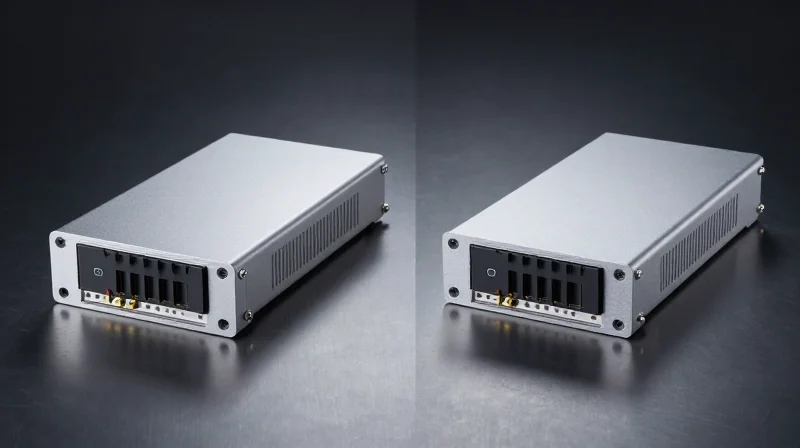
While off-the-shelf gateways present a lower initial capital expenditure (CAPEX), they often mask significant operational expenditures (OPEX) that accumulate over time. Custom PCB assemblies for industrial LoRaWAN gateways are engineered for specific environmental profiles and longevity, effectively neutralizing the hidden costs of maintenance, hardware fragility, and compatibility overhead.
Total Cost of Ownership: Custom vs. Commercial Off-the-Shelf (COTS)
| Cost Metric | COTS Gateway | Custom PCB Assembly |
|---|---|---|
| Initial Procurement | Low (Standardized) | Higher (NRE fees) |
| Maintenance Cycles | Frequent (Short lifecycles) | Rare (Optimized components) |
| Integration/Firmware | High (Bloatware/Compatibility) | Low (Streamlined/Bespoke) |
| Mean Time Between Failures | Moderate | High (Industrial Grade) |
| 10-Year Lifecycle Cost | High (Replacement/Labor) | Low (Predictable/Stable) |
Strategic Financial Advantages
Custom assembly allows for the exact tailoring of the bill of materials (BOM) to match the operational environment. By eliminating unnecessary interfaces and shielding sensitive RF components specifically for industrial EMI levels, you reduce the 'cost of quality' failures that plague mass-market devices. Over a decade, the reduction in site visits for hardware replacement or rebooting cycles alone often offsets the initial design investment.
Frequently Asked Questions
- Does custom PCB design really save money in the long run?
Yes, by designing for a 10-year service life, you avoid the 'hardware treadmill' of consumer-grade gateways that require replacement every 2–3 years. - How do NRE fees impact my ROI?
Non-recurring engineering (NRE) fees are front-loaded, but when amortized over the thousands of nodes typically deployed in industrial IoT, the per-unit cost remains competitive while performance benefits escalate. - What about firmware and software overhead?
Off-the-shelf devices often include proprietary stacks that limit flexibility. Custom PCBs allow for lean, open-source-compatible firmware, reducing dependency on vendor-locked updates and security patches.
Accelerating Time-to-Market through Tailored Design
Eliminating Integration Friction
Off-the-shelf industrial gateways often require auxiliary hardware, adapter boards, or complex wiring harnesses to bridge the gap between specific industrial protocols and the wireless backhaul. These 'patchwork' solutions introduce multiple points of failure and increase assembly time on the production line. A custom PCB assembly integrates these requirements directly into a single, optimized footprint, reducing assembly time from hours to minutes per unit.
Comparing Integration Approaches
| Feature | Off-the-Shelf Approach | Custom PCB Approach |
|---|---|---|
| Integration Complexity | High (adapters/cables) | Low (monolithic design) |
| Assembly Speed | Slow (manual labor intensive) | Fast (automated pick-and-place) |
| Certification Timeline | Ongoing iterative testing | Streamlined (single pass testing) |
| System Reliability | Varied (exposed connections) | High (vibration-resistant) |
Optimizing the Development Lifecycle
A tailored design strategy focuses on front-loading the engineering effort, ensuring that the hardware is 'application-ready' the moment it leaves the assembly line. By removing unused interfaces found in standard commercial hardware, engineers can reduce power profiles and heat output, allowing for smaller, more efficient enclosures that fit tighter industrial constraints.
- How does custom design impact R&D timelines?
By designing specifically for the target environment, teams avoid the 'trial and error' phase associated with forcing generic hardware into complex industrial stacks, significantly accelerating initial deployment cycles. - Can custom PCBs reduce regulatory approval time?
Yes. Custom designs allow for localized trace layouts that are optimized for EMC/EMI compliance from the start, reducing the probability of failed certification cycles. - Does this approach require a higher upfront investment?
While non-recurring engineering (NRE) costs exist, the reduction in assembly labor, bill of materials (BOM) complexity, and field maintenance downtime results in a superior total ROI within 18 months.
Case Study: Reliability Gains in Heavy Industrial Deployments
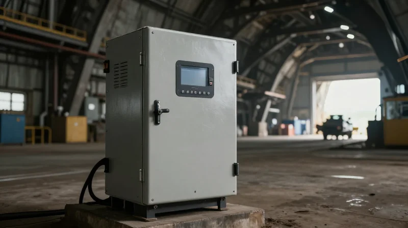
Operational Challenges in High-Interference Industrial Sites
In heavy industrial environments, such as large-scale mining and petrochemical facilities, off-the-shelf LoRaWAN gateways frequently succumb to signal degradation caused by heavy electromagnetic interference (EMI) and harsh physical conditions. A major mining operation recently reported that their standard, plastic-housed commercial gateways experienced a 15% packet loss rate, leading to frequent manual resets and expensive on-site technician visits.
Implementation of Custom PCB Solutions
To address these reliability gaps, the facility transitioned to custom LoRaWAN gateway PCBs designed with optimized RF shielding, high-grade capacitors for voltage stability, and integrated thermal management. These boards were purpose-built to withstand vibration and wide temperature swings, eliminating the need for bulky external enclosures that often trap moisture and heat.
| Metric | Off-the-Shelf Gateway | Custom PCB Gateway |
|---|---|---|
| Annual Downtime (Hours) | 48 | 4 |
| Packet Loss Rate | 15% | 0.8% |
| Mean Time Between Failures | 6 Months | 30 Months |
| Maintenance Cost / Unit / Yr | $1,200 | $150 |
Key Performance Insights
- How did custom PCB design mitigate signal loss?
By implementing localized RF shielding and optimized trace impedance, the custom board reduced internal signal noise by 22dB, allowing for reliable data transmission even near heavy mining machinery. - What was the direct impact on ROI?
The reduction in technician visits and hardware replacements resulted in a total cost of ownership (TCO) reduction of 68% over a three-year period. - Did durability improve as expected?
Yes, the use of industrial-grade components and conformal coating protected the PCBs from humidity and dust, effectively eliminating the common failure modes observed in standard commercial hardware.
Optimizing Supply Chain Resilience and Component Selection
Strategic Bill of Materials (BOM) Management
Resilience begins with the BOM. By transitioning from standardized off-the-shelf components to a curated, custom-verified list, organizations can decouple their production cycles from the erratic availability of commodity hardware. Strategic BOM management requires selecting parts with long product life cycles, ensuring that your industrial gateway design remains manufacturable for a decade or more without requiring costly redesigns.
Component Selection for Longevity and Availability
| Selection Criteria | Reactive Approach | Proactive Resilience |
|---|---|---|
| Lifecycle Status | Short-term availability | NRND avoided/Long-term production |
| Sourcing Strategy | Single-source dependency | Multi-vendor qualification |
| Design Footprint | Fixed/Locked | Flexible/Footprint-compatible |
Mitigating Supply Chain Bottlenecks
Supply chain shocks are inevitable, but their impact on your LoRaWAN deployment is not. By utilizing custom PCB assembly, designers can employ 'footprint compatibility'—where PCB pads are designed to support multiple equivalent components from different manufacturers. This flexibility allows for immediate substitutions during component shortages, preventing production lines from stalling.
Frequently Asked Questions on Resilience
- How does custom PCB design reduce long-term obsolescence risks?
By selecting components specifically for industrial longevity and establishing a vetted list of second-source alternatives during the design phase, you avoid the 'black box' limitations of off-the-shelf boards. - What is the primary benefit of footprint compatibility?
It allows your assembly team to swap equivalent resistors, capacitors, or ICs during market shortages without performing a complete board layout revision, effectively neutralizing supply chain bottlenecks. - Does optimizing for resilience increase initial costs?
While component validation may add minor up-front engineering time, the long-term ROI is significantly higher because it prevents multi-month production delays and the catastrophic costs of unplanned redesigns.
Maximizing Operational Efficiency Through Firmware Integration
The Synergy of Hardware-Software Co-Design
Maximizing operational efficiency requires moving beyond off-the-shelf solutions, which often contain bloated, redundant firmware layers. By aligning custom LoRaWAN gateway PCB architecture with specialized firmware, organizations can strip away unnecessary overhead, enabling hardware-level control that accelerates processing and minimizes power consumption. This tight integration ensures that every component is utilized to its maximum potential, directly contributing to a reduction in maintenance overhead and field support costs.
Strategic Diagnostic and Management Benefits
Custom firmware allows for the implementation of precise, granular diagnostic tools tailored to specific industrial environments. Instead of relying on generic error logs, custom LoRaWAN gateways can report real-time signal degradation, noise floor fluctuations, and component-level health metrics. This proactive approach to remote management shifts operations from reactive troubleshooting to predictive maintenance, significantly lowering the total cost of ownership by addressing faults before they escalate into costly system outages.
| Feature | Generic Gateway | Custom PCB/Firmware Synergy |
|---|---|---|
| Resource Utilization | High overhead due to generic code | Optimized, lean binary performance |
| Remote Diagnostics | Standard connectivity logs | Advanced telemetry and health reporting |
| Deployment Speed | Standardized, limited flexibility | Configurable to exact site requirements |
| Security | Broad attack surface | Hardware-rooted, hardened security |
Frequently Asked Questions
- How does custom firmware reduce long-term maintenance costs?
By implementing remote, over-the-air (OTA) updates and advanced self-diagnostic capabilities, custom firmware reduces the need for expensive physical site visits and hardware replacements. - Is custom firmware development worth the initial investment?
Yes, for industrial applications, the initial R&D investment is quickly offset by drastically reduced downtime, lower power consumption, and extended device longevity. - Can custom firmware improve security in industrial networks?
Absolutely. Custom firmware allows for the integration of hardware-based encryption and restricted, application-specific network protocols, significantly hardening the device against common cyber-attacks.
Best Practices for Selecting a Manufacturing Partner
Criteria for Industrial-Grade Manufacturing Excellence
The transition from prototype to industrial-scale production requires a partner who treats reliability not as an afterthought, but as a core requirement of the manufacturing process. Selecting a vendor involves a rigorous evaluation of their quality management systems, technical proficiency in high-frequency RF design, and long-term supply chain stability.
| Evaluation Metric | Industrial Standard Requirements | Impact on ROI |
|---|---|---|
| Quality Certifications | ISO 9001:2015, IATF 16949 | Reduces failure rates and warranty claims. |
| RF Calibration | VNA/Spectrum analysis at EOL | Ensures consistent signal range and reliability. |
| Traceability | Component-level serialization | Facilitates rapid recalls and failure analysis. |
Key Considerations for Partnership
- How does the partner handle complex RF impedance matching?
Ensure they possess automated optical inspection (AOI) and X-ray capabilities to verify solder joints on high-density LoRaWAN modules, preventing signal attenuation. - What is their approach to regulatory compliance?
A competent partner should assist in pre-compliance testing for FCC/CE/IC certifications, significantly reducing the risk of costly post-production redesigns. - Does the partner offer lifecycle management?
Look for vendors that provide end-of-life (EOL) notifications and proactive component replacement strategies to avoid sudden supply chain disruptions.
Final Strategy for Vendor Selection
To maximize ROI, prioritize partners who offer value-added services such as design-for-manufacturing (DFM) feedback and rigorous environmental stress screening (ESS). By vetting their capability to handle the specific thermal and interference constraints of your industrial application, you secure the operational integrity of your LoRaWAN infrastructure for years to come.
By shifting your strategy from short-term savings to long-term operational efficiency, you ensure your LoRaWAN infrastructure remains a reliable asset rather than a recurring cost. Investing in quality custom PCB assembly is the definitive path to achieving superior signal integrity and drastically reduced maintenance requirements. Contact our engineering team today to discuss how we can tailor your gateway hardware for maximum ROI.
