
In the competitive landscape of modern electronics, every square millimeter of PCB real estate directly translates to either profit or loss. As device miniaturization accelerates, designers face a critical decision: how to achieve high-density routing without ballooning fabrication costs. The strategic implementation of blind and buried vias offers a sophisticated solution to this challenge, enabling smaller form factors and streamlined assembly processes.
Understanding the Role of Interconnect Complexity
The Interconnect Density Challenge
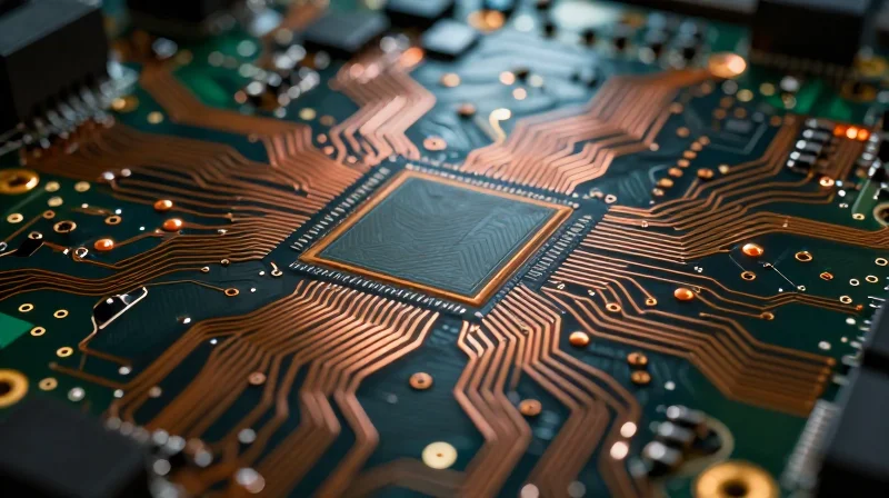
Interconnect complexity is the primary constraint in modern PCB design, acting as a bottleneck for both miniaturization and performance. As component pin densities escalate—particularly with fine-pitch BGAs—the traditional reliance on through-hole vias creates significant routing congestion. This congestion forces designers to add layers to the stack-up to maintain signal paths, which drives up production costs and complicates assembly. By leveraging advanced via architectures, such as microvias and blind/buried vias, designers can reclaim valuable board real estate, effectively reducing the necessary layer count and shrinking the overall PCB footprint.
Comparing Via Technologies
| Via Type | Routing Density | Signal Integrity | Cost Impact |
|---|---|---|---|
| Through-Hole | Low | Moderate (Stub issues) | Low (Standard) |
| Blind/Buried | High | High | Moderate |
| Stacked Microvia | Very High | Excellent | High (Precision req.) |
Strategic Impact on Signal Integrity
Beyond physical dimensions, via technology is a critical determinant of signal integrity. Through-hole vias often result in long barrels that act as stubs, introducing unwanted reflections and resonance at high frequencies. Advanced via technologies like laser-drilled microvias allow for shorter interconnects, significantly reducing parasitic capacitance and inductance. This transition not only enhances high-speed performance but also simplifies the routing topology, allowing for shorter trace lengths and improved impedance control.
Key Considerations for Implementation
- How do microvias reduce assembly costs?
By increasing routing density per layer, microvias allow for a reduction in total board layers, directly lowering material costs and the complexity of the lamination cycle. - Do advanced vias negatively impact yield?
While they require tighter manufacturing tolerances, advanced via structures often lead to higher overall yields by reducing the likelihood of shorts and opens caused by excessive, congested via-in-pad transitions. - What is the ROI threshold for transitioning to HDI?
The ROI becomes clear when the cost savings from reduced layer counts and decreased board area outweigh the premium costs of laser-drilling and sequential lamination processes.
The Economics of PCB Miniaturization
The Economic Impact of Footprint Reduction
Miniaturization is not merely a design objective; it is a financial strategy. By utilizing advanced via technologies—such as laser-drilled microvias, blind/buried vias, and via-in-pad—engineers can drastically reduce the physical footprint of a circuit board. This reduction allows more PCB units to fit onto a single standard manufacturing panel, directly lowering the cost-per-board (CPB) of the raw laminate material and significantly decreasing the overhead of multi-pass fabrication.
| Metric | Standard Via Design | Advanced Microvia Design |
|---|---|---|
| Panel Utilization | 65-75% | 85-95% |
| Raw Material Usage | Baseline | 20-40% Reduction |
| Manufacturing Passes | High | Optimized |
Key Economic Considerations
- How does via density impact panel waste?
Lower via density requires larger keep-out zones and routing areas, forcing a larger overall board size. Advanced microvias enable higher routing density in a smaller area, improving the 'net-to-panel' ratio. - Does high-density via technology increase assembly costs?
While fabrication cost per square inch increases with HDI complexity, the total system cost often drops due to reduced board size, fewer layers required, and the ability to fit into smaller, less expensive enclosures. - What is the primary ROI driver in volume production?
The multiplier effect of panel utilization is the primary driver. Increasing the count of PCBs per panel by even 10% can lead to substantial annual savings in high-volume production environments.
Ultimately, the transition to advanced via interconnects shifts the cost burden from raw material waste to intelligent design. By consolidating signal layers and minimizing PCB real estate, companies can achieve higher yields per panel, ensuring that the initial investment in higher-technology fabrication is quickly offset by the economies of scale achieved through footprint optimization.
Blind and Buried Vias: Technical Fundamentals
Defining Blind and Buried Vias
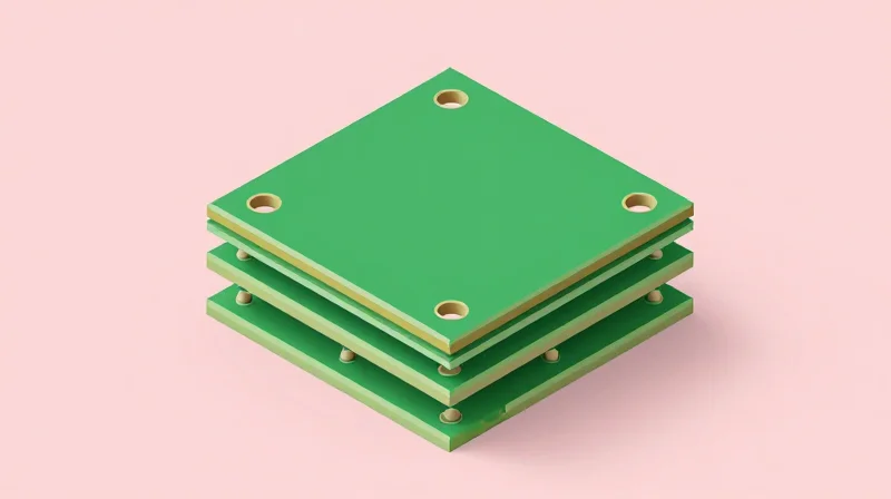
Blind and buried vias represent a shift from traditional through-hole drilling methods, which traverse the entire board thickness. A blind via connects an outer layer to an internal layer but does not penetrate the entire board, while a buried via connects two or more internal layers without reaching the external surfaces. These interconnects are essential for high-density interconnect (HDI) designs, as they clear routing paths on signal layers that would otherwise be blocked by through-hole pads.
Technical Comparison of Via Architectures
| Via Type | Layer Access | Primary Benefit |
|---|---|---|
| Through-Hole | All Layers | Lowest manufacturing cost |
| Blind Via | Outer + Inner | Saves top/bottom surface area |
| Buried Via | Inner Layers Only | Maximizes internal routing density |
Impact on Design and Assembly
By moving away from through-hole vias, designers can reduce the number of signal layers required, potentially lowering total board thickness and raw material costs. Furthermore, since blind and buried vias are typically laser-drilled or micro-via based, they support finer pitch component placement, such as Fine Pitch Ball Grid Arrays (FBGA), which are otherwise impossible to route on standard through-hole boards.
- How do these vias affect signal integrity?
These vias reduce parasitic capacitance and inductance by minimizing via stub lengths, which is critical for high-speed signal propagation. - What are the primary manufacturing constraints?
Blind and buried vias require sequential lamination processes, which increase board fabrication cycle time and cost compared to standard manufacturing. - When is it cost-effective to transition to advanced vias?
The ROI becomes positive when the reduced layer count and board size lead to lower overall material costs or enable a higher number of boards per production panel.
Real-World Case Study: Improving Lifecycle Performance
Case Study: Industrial IoT Sensor Redesign
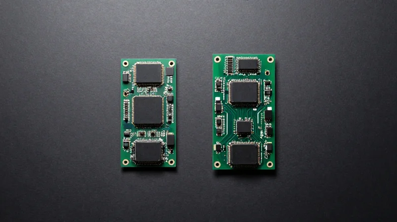
A leading industrial IoT manufacturer faced significant challenges with a legacy PCB design for their vibration monitoring unit. The original board, reliant on traditional through-hole vias, suffered from excessive footprint size and poor thermal dissipation during 24/7 operation in harsh environments. By migrating to a high-density interconnect (HDI) architecture utilizing stacked micro-vias, the engineering team achieved a 35% reduction in PCB surface area and a 15% increase in Mean Time Between Failures (MTBF).
| Metric | Legacy Design (Through-Hole) | Advanced Design (Stacked Micro-Vias) | Improvement |
|---|---|---|---|
| Board Footprint | 120 cm² | 78 cm² | 35% Reduction |
| Layer Count | 8 Layers | 6 Layers | 25% Efficiency |
| Thermal Resistance | 42 °C/W | 31 °C/W | 26% Reduction |
Key Performance Insights
- How did micro-vias improve thermal performance?
By utilizing stacked micro-vias, the design created efficient thermal paths directly from high-heat components to internal ground planes, lowering the junction temperature of critical ICs. - What was the impact on assembly costs?
Although the fabrication cost per square inch increased, the reduced layer count and the elimination of extraneous signal routing allowed for higher panel utilization, resulting in a net 12% lower assembly cost per unit. - Why did product longevity increase?
Reducing the mechanical stress on the PCB through smaller, laser-drilled vias decreased the occurrence of micro-cracks during thermal cycling, directly extending the sensor's lifecycle in the field.
The transition to advanced via technology demonstrated that ROI is not merely a function of material reduction. By optimizing signal paths through HDI techniques, the manufacturer successfully minimized inductive crosstalk and improved power integrity, proving that advanced via selection is a strategic tool for enhancing product lifecycle performance.
Reducing Assembly Complexity and Failure Points
Optimizing Component Density via Via-in-Pad
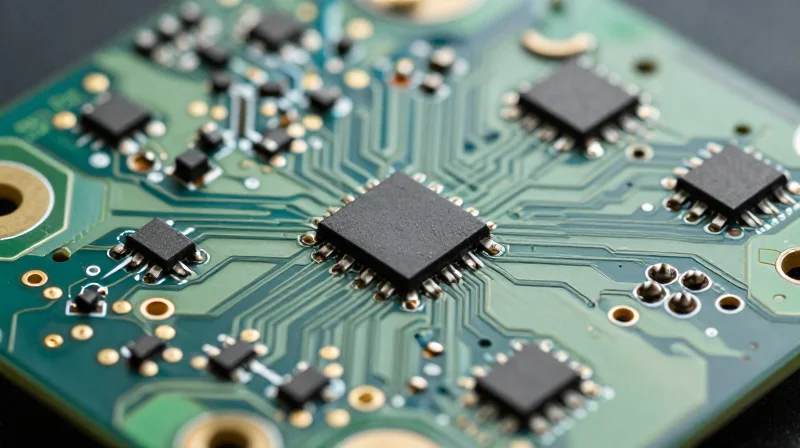
Traditional through-hole via design often forces a physical separation between the component pad and the routing trace, leading to increased trace lengths and routing congestion. By utilizing Via-in-Pad (VIP) technology, engineers can place vias directly underneath the mounting pad. This eliminates 'dog-bone' escape routing, significantly reducing the surface area required for connectivity and allowing for higher component density on smaller board footprints.
Impact on Assembly and Manufacturing Reliability
Complex routing paths often increase the risk of solder bridges and tombstoning during reflow. Advanced via placement strategies facilitate cleaner signal paths, which minimizes parasitic inductance and simplifies the thermal profile of the PCB. When vias are properly plugged and capped (via-in-pad plated over), they provide a flat surface that improves the structural integrity of the solder joint and prevents solder wicking, a primary cause of assembly failure.
| Via Type | Escape Routing Density | Assembly Complexity | Primary Benefit |
|---|---|---|---|
| Standard Through-Hole | Low | High | Lowest Cost |
| Blind/Buried Vias | Medium | Moderate | Increased Layer Efficiency |
| Via-in-Pad (VIP) | Very High | Low | Superior Signal Integrity |
Frequently Asked Questions
- How does Via-in-Pad reduce assembly defects?
By plating over the via, the pad surface becomes flat, preventing solder from draining into the via hole during reflow, which ensures a consistent and strong solder joint. - Does switching to advanced vias increase production costs?
While unit board costs may increase due to specialized drilling and plating processes, the overall ROI is typically higher because it reduces assembly rework and allows for a smaller, more cost-efficient PCB footprint. - Are there limits to via-in-pad density?
Density is limited primarily by the PCB fabricator's drill-to-copper registration capabilities and the thickness of the board, which dictates the aspect ratio requirements for reliable plating.
Design for Manufacturing (DFM) Best Practices
Strategic DFM Guidelines for Advanced Vias
The successful integration of blind and buried vias relies on balancing electrical performance requirements with the capabilities of your fabrication house. By optimizing aspect ratios and plating standards early in the design cycle, engineers can significantly reduce yield loss and manufacturing lead times.
| Parameter | Standard Constraint | DFM Recommendation |
|---|---|---|
| Aspect Ratio | 10:1 | Limit to 6:1 for high-yield |
| Via Diameter | 0.25mm | Minimize to 0.15mm with laser drill |
| Annular Ring | 0.1mm | Ensure 0.05mm min per IPC-2221 |
Optimizing for Assembly Costs
When incorporating HDI features, placement accuracy remains the greatest cost driver. Always verify that via-in-pad (VIPPO) structures are properly filled and capped to prevent solder wicking, which can cause intermittent shorts during the reflow process.
Frequently Asked Questions
- How do I minimize fabrication costs?
Stick to standard stack-up sequences and avoid staggered via patterns whenever possible, as complex layer-to-layer connections increase the number of drilling and lamination cycles. - Why should I use conductive epoxy for via filling?
Conductive filling provides superior thermal dissipation and planar surface integrity, allowing components to be placed directly over the via without risking solder voids. - What is the impact of via density on board cost?
Excessive via density increases the number of drill hits, which elevates machine time and tool wear charges. Optimize your fan-out to use the fewest vias required for signal integrity.
Calculating Your Return on Investment (ROI)

The ROI Framework for Advanced Via Integration
Transitioning from standard thru-hole or simple blind/buried vias to HDI (High-Density Interconnect) structures like via-in-pad or laser-drilled microvias requires a shift in how you evaluate PCB procurement. While unit costs per board often increase due to complex drilling and plating sequences, the aggregate ROI is realized through footprint reduction, which lowers raw material usage and enables smaller, more efficient device enclosures.
Cost-Benefit Comparison
| Metric | Standard Via Design | Advanced Via (HDI) Design |
|---|---|---|
| Board Size | Larger (Baseline) | 15%–40% Reduction |
| Layer Count | Higher | Lower (via density increase) |
| Assembly Yield | Moderate | Higher (reduced congestion) |
| Unit Cost | Lower | Higher |
Calculating the Break-Even Point
To determine when advanced via technology pays for itself, use a total cost of ownership (TCO) model. The formula should account for the reduction in PCB surface area—which lowers laminate costs—and the savings gained from fewer layers required to achieve equivalent signal routing.
ROI = [(Total Savings in Assembly + Saved Material Costs) - (Added Manufacturing Complexity Premiums)] / (Total Initial Investment)- How do I account for yield improvements in my ROI calculation?
Factor in the reduction of rework cycles and scrap rates. Because via-in-pad technologies reduce signal path congestion, SMT assembly defects are statistically lower, leading to higher first-pass yields. - Is the ROI immediate?
No. The initial prototyping phase often incurs a 'complexity tax.' Real ROI typically manifests once you transition to high-volume production, where the per-unit material savings and improved assembly throughput outweigh the NRE costs. - What is the biggest hidden saving?
Product longevity and thermal reliability. By minimizing failure points and optimizing thermal dissipation, you reduce warranty claims and field returns, which are often the most significant but overlooked costs in hardware lifecycles.
By leveraging blind and buried vias, engineering teams can achieve superior density and efficiency, ultimately driving down costs and improving performance at scale. Don't let outdated routing techniques hold your product back. Contact our design experts today to review your board layout and start optimizing for your next high-volume production run.
