
In the cutthroat world of next-generation networking, the margin between market dominance and obsolescence often lies in the efficiency of the printed circuit board. As WiFi 7 introduces unprecedented data throughput, engineers face the dual pressure of mitigating complex signal interference and managing soaring fabrication costs. This article explores how data-driven design optimizations are reshaping the economics of high-speed hardware manufacturing.
The WiFi 7 Manufacturing Challenge: Balancing Speed and Scale

The Physical Layer Constraint of WiFi 7
WiFi 7 (IEEE 802.11be) elevates throughput capabilities through 320 MHz channels and 4K-QAM modulation, placing unprecedented strain on PCB fabrication. At these higher frequencies and tighter signal margins, even microscopic defects in dielectric materials or copper trace geometry can result in catastrophic signal loss and decreased ROI.
Manufacturing Complexity Metrics
| Parameter | WiFi 6/6E Standard | WiFi 7 Requirement | Manufacturing Impact |
|---|---|---|---|
| Max Bandwidth | 160 MHz | 320 MHz | Higher spectral purity required |
| Modulation | 1024-QAM | 4096-QAM | Stringent signal-to-noise ratio |
| Insertion Loss | Standard Tolerance | Ultra-low tolerance | Advanced substrate materials |
Balancing High-Speed Performance with Cost-Efficiency
Manufacturers face a dual challenge: the necessity for specialized, low-loss laminate materials versus the commercial requirement for competitive pricing. To achieve economies of scale, production lines must shift toward automated optical inspection (AOI) and refined etching processes that minimize impedance discontinuities without relying on prohibitively expensive bespoke substrate stacks.
Common Industry Questions
- Why does 4096-QAM increase PCB manufacturing difficulty?
4096-QAM requires an incredibly clean signal path; even minor trace surface roughness or dielectric inconsistencies create phase noise that prevents the receiver from correctly demodulating the dense signal constellation. - Can standard FR-4 substrates support WiFi 7?
Generally, no. Standard FR-4 exhibits excessive dielectric loss at WiFi 7 operating frequencies, necessitating the use of specialized high-frequency, low-loss laminate materials that challenge traditional cost models. - What is the biggest driver of ROI loss in MIMO PCB production?
Yield degradation due to signal integrity failures at the final testing stage is the primary driver. Minimizing scrap rates through tighter process control early in the etching and lamination phases is essential for profitability.
Identifying the Hidden Costs of Signal Interference

The Financial Impact of EMI and Crosstalk
In advanced MIMO router manufacturing, signal integrity is synonymous with yield. When Electromagnetic Interference (EMI) shielding is inadequate or trace coupling exceeds design tolerances, crosstalk occurs, leading to performance degradation in high-frequency bands. These technical failures manifest immediately on the production line as high scrap rates, as defective boards often cannot be reworked economically. Furthermore, the need for exhaustive end-of-line testing to isolate these intermittent signal faults extends cycle times, directly eroding your Return on Investment.
| Failure Mechanism | Primary Production Impact | Economic Consequence |
|---|---|---|
| Inadequate EMI Shielding | High EMI test failure rates | Increased WIP and material scrap |
| Excessive Trace Crosstalk | Signal throughput instability | Extended calibration and testing time |
Hidden Cost Drivers in Production
- Why does crosstalk increase testing costs?
Crosstalk often creates intermittent signal failures that are difficult to diagnose. This forces manufacturers to implement multi-stage testing, which lengthens production lead times and consumes expensive RF testing equipment capacity. - How do shielding defects impact ROI?
Substandard shielding results in non-compliant units that fail regulatory and performance testing. The cost isn't just the board itself, but the lost labor, overhead, and throughput capacity spent on manufacturing a board destined for the scrap heap.
To mitigate these costs, manufacturers must transition from reactive testing to proactive design validation. Integrating automated optical inspection for shield placement and utilizing advanced simulation software to predict crosstalk during the CAM phase ensures that issues are resolved long before the board reaches the physical assembly line, thereby maximizing ROI.
Strategic PCB Stack-up Optimization for Cost Efficiency

Optimizing a PCB stack-up for advanced MIMO routers is a balancing act between physical space, thermal dissipation, and signal integrity. By transitioning from high-layer-count designs to more compact configurations through advanced routing densities, manufacturers can drastically lower material expenses and improve yield rates. This strategy hinges on moving away from 'blindly adding planes' toward precision signal path management.
Reducing Layer Count via Micro-via Technology
Traditional multi-layer boards often suffer from 'layer inflation' due to inefficient trace routing. By utilizing HDI (High-Density Interconnect) techniques—specifically micro-vias and via-in-pad technology—designers can consolidate multiple signal layers into a single, optimized routing layer. This not only reduces the total board thickness and copper weight but also minimizes the drill cycle time, which is a major contributor to production costs.
| Strategy | Cost Impact | Signal Integrity Benefit |
|---|---|---|
| Standard Thru-hole | High (More layers) | Low (High parasitic) |
| HDI Micro-via | Medium (Reduced layer) | High (Better impedance) |
| Back-drilling | High (Complexity) | Optimal (Reduces stubs) |
Strategic Material Selection
Material costs in WiFi 7 equipment are driven by the need for low-loss laminates. Instead of using expensive high-frequency laminates throughout the entire stack, a hybrid stack-up strategy—where high-performance material is relegated to the outer critical signal layers and standard FR-4 or mid-tier laminates are used for internal power/ground cores—can optimize ROI without degrading MIMO performance.
Frequently Asked Questions on Stack-up Optimization
- Does reducing layer count increase crosstalk?
Not necessarily; if routing density increases, crosstalk must be managed through stricter isolation guidelines and better field solver modeling, which is cheaper than the cost of extra physical layers. - How does HDI affect production cycle time?
While laser drilling adds a process step, it eliminates the need for mechanical drill passes across 10-12+ layers, often leading to a net reduction in overall fabrication time and scrap rates. - Is hybrid stack-up reliable for long-term thermal cycling?
Yes, provided the Coefficient of Thermal Expansion (CTE) of the chosen laminate materials is carefully matched to prevent delamination and barrel cracking.
Case Study: Streamlining MIMO Antenna Array Design
Project Overview: Optimizing the MIMO Antenna Array
A leading networking hardware manufacturer faced mounting pressure from rising component costs and high scrap rates in their next-generation WiFi 7 MIMO router production. The design was plagued by excessive signal loss due to complex trace routing and high component counts in the RF front-end, necessitating an immediate intervention to maintain profit margins.
Implementation Strategy
The engineering team employed a three-pronged approach to address the technical and financial bottlenecks:
- Component Consolidation
Replaced discrete surface-mount matching components with integrated, multi-functional RF modules, reducing the total component count by 22%. - Trace Geometry Refinement
Adopted high-precision controlled-impedance routing to minimize signal reflections, allowing for thinner dielectric layers without sacrificing signal integrity. - Via Structure Optimization
Transitioned to blind/buried via technology to free up board surface area, allowing for a more compact antenna placement that shortened total path lengths.
Performance and Cost Comparison
| Metric | Original Design | Optimized Design |
|---|---|---|
| Total Component Count | 142 | 111 |
| Signal Insertion Loss (dB) | -2.8 | -1.9 |
| Unit Production Cost | Baseline | -15% Reduction |
Key Takeaways for Future Design
- Can consolidation increase yield?
Yes, by reducing the number of pick-and-place operations, we significantly lowered the potential for solder-related defects and improved overall first-pass yield. - How does signal loss relate to ROI?
Minimizing signal loss reduces the need for expensive high-frequency substrate materials and decreases testing time, directly lowering the per-unit cost.
Material Selection and Its Impact on Long-term Profitability
Strategic Material Selection for MIMO Routers
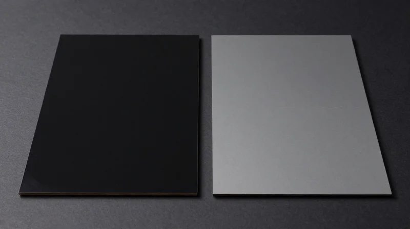
In mass-market MIMO router production, the dielectric material is the primary cost driver and the most critical factor for signal integrity. Choosing between standard FR-4, mid-range high-speed laminates, and ultra-low-loss PTFE-based materials requires a precise understanding of the router's operating frequency. Selecting a material that is 'over-engineered' for the required data rate results in unnecessary material expenses, while choosing low-cost, high-loss materials leads to failed compliance testing, higher scrap rates, and field failures.
| Material Class | Signal Performance | Cost Index | Best Use Case |
|---|---|---|---|
| Standard FR-4 | Low | 1.0x | Low-frequency routers |
| Modified Epoxy (Mid-Loss) | Moderate | 1.5x - 2.0x | Wi-Fi 6/6E consumer routers |
| PTFE/Ceramic Filled | Very High | 3.5x - 5.0x | High-end enterprise MIMO arrays |
Balancing Performance and Production Yield
Profitability is not merely the cost of raw copper and substrate; it is defined by the total yield of the manufacturing process. Modern MIMO designs often rely on strict impedance control. Higher-performing materials with lower moisture absorption rates often reduce the need for expensive post-production drying processes and improve stability during the reflow process, ultimately lowering the total cost of ownership by increasing the number of good boards per panel.
- How does material selection affect signal loss?
Materials with lower Dissipation Factor (Df) reduce signal attenuation over long trace runs, allowing for thinner copper traces or fewer layers while maintaining the signal budget required for MIMO performance. - Can switching to cheaper laminates increase costs?
Yes. If the laminate's thermal expansion coefficient (CTE) does not match the process requirements, it leads to via barrel cracking during assembly, significantly increasing scrap rates and rework costs. - Is hybrid board construction a viable cost-saving measure?
Hybrid stack-ups, which use high-frequency laminates for critical signal layers and cost-effective FR-4 for inner routing or power planes, offer the most balanced ROI for complex multi-antenna MIMO systems.
Implementing Design for Manufacturing (DFM) Protocols
Integrating DFM to Mitigate MIMO Interference
DFM is no longer an optional review step; for complex MIMO architectures, it is a critical gatekeeping process. By establishing manufacturing constraints—such as minimum trace-to-plane clearances and via-stitching requirements—directly within the CAD environment, engineers can identify signal integrity bottlenecks before a single prototype is ordered. This proactive approach standardizes the transition from design to fabrication, ensuring that high-speed traces are optimized for impedance matching while simultaneously adhering to cost-effective production tolerances.
Key DFM Constraints for High-Frequency Routers
| Design Parameter | Manufacturing Constraint | Impact on ROI |
|---|---|---|
| Trace Spacing | Maintain >3x dielectric height | Prevents crosstalk, avoids board scrap |
| Via Placement | Strict antipad geometry | Reduces signal reflections, improves yield |
| Copper Weight | Uniform 0.5 oz to 1 oz usage | Minimizes etching time and chemical cost |
Frequently Asked Questions
- How does early DFM improve ROI?
Early detection of layout issues allows for corrections in software, avoiding the massive sunk costs of scrapping faulty physical PCBs and repeating fabrication cycles. - Does stricter DFM increase manufacturing costs?
Paradoxically, no. While high-precision tolerances are required, standardizing the design library reduces the 'special handling' surcharges that fabricators apply to non-standard or 'difficult' board files. - What is the primary benefit for MIMO arrays?
Consistent DFM ensures that parasitic capacitance and inductance remain within simulation parameters, which is vital for maintaining the phase alignment necessary for high-performance MIMO throughput.
The ROI of Advanced Simulation Tools

The Economic Imperative of Simulation-Driven Design
In the context of high-performance MIMO router manufacturing, the cost of a single board-level re-spin often exceeds the initial licensing fees of professional-grade simulation software. By migrating from 'build-and-test' methodologies to virtual prototyping, engineering teams can validate signal impedance, crosstalk, and thermal management in a synthetic environment, effectively eliminating the primary drivers of hardware iteration delays.
Comparative Cost Impact of Prototyping Approaches
| Parameter | Physical Prototyping Cycle | Simulation-Driven Design |
|---|---|---|
| Typical Lead Time | 3-6 Weeks | 2-5 Days (Virtual) |
| Cost per Iteration | High (Fabrication & Assembly) | Low (Compute Resource) |
| Error Detection | Late (Post-Fabrication) | Early (Pre-Fabrication) |
Key Advantages for MIMO Signal Integrity
Advanced simulation platforms allow for the granular analysis of MIMO antenna arrays, which are notoriously sensitive to parasitic coupling. By precisely predicting these interactions, designers can optimize trace length and shielding without needing physical testing to confirm performance targets.
- How does simulation impact ROI?
It reduces the number of physical hardware iterations, which are the most expensive stage of the development lifecycle due to fabrication, shipping, and testing labor. - Can simulation predict long-term field reliability?
Yes, by modeling thermal stress and power integrity, engineers can simulate aging effects, ensuring the device meets longevity requirements without needing extensive destructive testing. - Is the learning curve worth the investment?
While training costs exist, the ability to iterate at the speed of software allows firms to accelerate time-to-market, providing a competitive advantage that quickly offsets tool overhead.
Future-Proofing Your Hardware Production Strategy
Anticipating Next-Generation Connectivity Standards
As MIMO technology evolves toward higher order antenna arrays and ultra-wideband spectrum utilization, the physical layer constraints become increasingly unforgiving. Future-proofing necessitates shifting focus from today's performance benchmarks to the modular requirements of upcoming standards like Wi-Fi 7 and 6G. Production strategies must prioritize material scalability and advanced interconnect integrity to avoid obsolescence before the product lifecycle concludes.
Strategic Alignment: Design and Manufacturing Collaboration
To mitigate the risk of signal degradation in high-density MIMO routers, the silo between RF design engineers and fabrication facilities must be dismantled. Early-stage joint engineering reviews are no longer optional but a critical component of ROI protection.
| Strategy Phase | Reactive Approach | Future-Proof Approach |
|---|---|---|
| Material Selection | Short-term cost optimization | Standardized multi-tier RF substrate portfolio |
| Design Review | Post-layout validation only | Concurrent RF/DFM collaborative modeling |
| Production Scalability | Single-vendor dependency | Cross-vendor validated production templates |
Frequently Asked Questions on Future-Proofing
- How does modularity improve ROI?
Modular designs allow for upgrading RF front-end components without requiring a complete PCB re-spin, significantly reducing time-to-market and tooling costs for iterative releases. - Why is material standardization critical?
Standardizing on a limited range of high-frequency laminates allows for better volume pricing with material suppliers and ensures consistent performance characteristics across multiple production batches. - What is the role of digital twins in this strategy?
Digital twins bridge the gap between design and physical fabrication, allowing for real-time adjustments to manufacturing tolerances that account for dielectric variations before a single prototype is cut.
Achieving profitability in the high-speed networking market requires moving beyond traditional design methodologies to embrace a holistic approach where cost-efficiency and performance are engineered in tandem. By refining PCB stack-ups and prioritizing DFM practices, manufacturers can ensure their WiFi 7 products lead the market in both capability and margin. Ready to optimize your next production run? Contact our engineering team today for a comprehensive design-for-cost audit.
