
In the cutthroat landscape of high-speed networking, the margin between market leadership and obsolescence is often found on the assembly line. As data rates climb and tolerances tighten, manufacturers face mounting pressure to reconcile aggressive cost targets with the rigid performance demands of optical transceivers. This article explores how strategic PCBA integration transforms these challenges into a competitive advantage, proving that reliability and cost-efficiency are not mutually exclusive.
The Economics of Modern PCBA Assembly in Networking
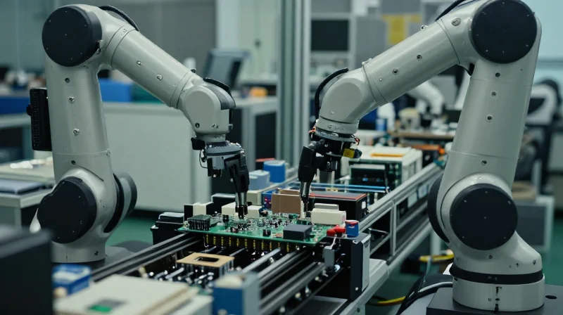
The Erosion of Traditional Assembly Economics
Traditional PCBA manufacturing models are increasingly ill-equipped to handle the requirements of 400G, 800G, and future-generation optical transceivers. As signal integrity becomes paramount, the cost of iterative prototyping and manual assembly labor is rising exponentially. The primary failure of legacy approaches lies in the inability to manage thermal density and parasitic capacitance effectively during high-volume production, leading to higher rejection rates and hidden yield-loss costs.
Critical Cost Drivers in High-Speed Module Production
| Cost Driver | Impact on ROI | Mitigation Strategy |
|---|---|---|
| Material Scrap | High | Advanced Solder Paste Printing |
| Manual Inspection | Moderate | Automated Optical Inspection (AOI) |
| Signal Integrity Rework | Extreme | Integrated SI/PI Simulation |
| Thermal Management | High | Precision Heat Sink Integration |
Strategic Shifts for Enhanced ROI
Maximizing ROI requires moving beyond simple per-unit pricing and focusing on Total Cost of Ownership (TCO). By integrating advanced assembly techniques such as fine-pitch flip-chip mounting and rigorous substrate characterization, manufacturers can significantly reduce latent defects that surface during final testing. This shift requires up-front investment in design-for-manufacturing (DFM) tools, which pays dividends by accelerating time-to-market and stabilizing yield consistency.
- Why do traditional PCBA assembly methods struggle with current optical transceivers?
They lack the precision required for tight tolerance margins and fail to optimize for the extreme thermal and signal interference levels prevalent in high-speed optical networking. - How does advanced integration directly influence ROI?
Through minimized yield loss, reduced rework cycles, and superior product longevity, manufacturers can extract more value from the production line while maintaining competitive market pricing.
Identifying the Hidden Costs of Yield Loss

The Anatomy of Yield Loss in High-Speed Optics
Yield loss in optical transceiver PCBA assembly is rarely the result of a single catastrophic event; rather, it is the cumulative effect of marginal design decisions failing to account for high-frequency signal integrity and thermal dissipation requirements. When DFM principles are ignored, the integration process becomes susceptible to microscopic defects that only emerge during final optical power-up or high-temperature stress testing.
| Failure Category | Primary Trigger | Impact on ROI |
|---|---|---|
| Signal Integrity Degradation | Improper trace impedance/Via stub | High rework/Scrap rate |
| Thermal Delamination | Inconsistent PCB stack-up/CTE | Field failure/Warranty costs |
| Optical Misalignment | Tolerance stack-up in housing | Low first-pass yield |
Hidden Financial Drivers
The financial impact extends beyond the immediate scrap value of a defective unit. Manufacturers often overlook the 'shadow costs' of yield loss, which include capacity bottlenecking and extended quality assurance cycle times. When failure rates exceed the standard deviation of an optimized line, engineering teams are diverted from product innovation to perform forensic failure analysis, effectively doubling the R&D cost per unit produced.
- Why does rework sometimes cost more than scrap?
Rework introduces thermal stress to high-speed components, potentially causing latent defects that pass immediate tests but fail in the field, leading to catastrophic reputational damage. - How does PCB stack-up impact optical transceiver yield?
Inaccurate stack-up design directly affects impedance control on high-speed differential pairs; deviations as small as 5% can cause eye-pattern closure, rendering the optical engine non-compliant. - Can DFM integration mitigate these costs?
Yes, by integrating optical alignment tolerances into the initial PCB layout and utilizing automated optical inspection (AOI) specifically calibrated for transceiver geometry, manufacturers can capture defects at the earliest possible stage.
Design for Manufacturing (DFM) Best Practices
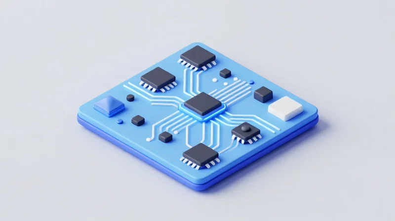
Synchronizing Signal Integrity with SMT Yield
The primary challenge in modern optical transceiver assembly lies in balancing the stringent electromagnetic requirements of high-speed differential pairs with the physical constraints of Surface Mount Technology (SMT) processes. Optimizing the PCBA requires a shift toward 'design-for-assembly-first' workflows, where pad geometry, trace routing, and thermal relief patterns are finalized prior to electrical sign-off.
| Parameter | Signal Integrity Impact | Manufacturing Impact |
|---|---|---|
| Via-in-Pad | Minimized parasitic inductance | Risk of solder wicking and voids |
| Thermal Relief | Potential impedance discontinuity | Improved reflow consistency |
| Trace Symmetry | Balanced propagation delay | Reduced stencil aperture complexity |
Key DFM Optimization Strategies
- Optimizing Land Patterns
Utilize IPC-7351 standard footprints modified for high-frequency signal propagation; specifically, adjust copper pullback to prevent solder bridging while maintaining consistent impedance profiles. - Thermal Management Consistency
Avoid large copper planes connected directly to small SMT pads, as these act as heat sinks that prevent uniform reflow, leading to cold solder joints or tombstoning. - Stackup Symmetry
Ensure substrate stackup is balanced to prevent PCB warpage during high-temperature reflow cycles, which is essential for maintaining alignment in high-density BGA packages.
Frequently Asked Questions
- How does via-in-pad affect signal integrity?
While via-in-pad is necessary to save space for high-speed routing, it can introduce signal discontinuities; proper plugging and capping processes are required to ensure both electrical performance and manufacturing reliability. - Can DFM measures increase total cost of ownership?
Initially, yes; however, the upfront investment in DFM analysis significantly reduces long-term costs by eliminating the high expense associated with scrap, rework, and field failures.
Strategic Component Selection for Longevity
Substrate Material Selection: Balancing Performance and Longevity
The choice of base material directly dictates signal loss, thermal dissipation, and mechanical stability at high frequencies. Transitioning from standard FR-4 to advanced low-loss laminates like polyimide or specialized PTFE-based substrates is essential for mitigating dielectric loss and ensuring consistent impedance matching over the module's lifespan.
| Substrate Type | Thermal Conductivity | Signal Integrity (High Freq) | Cost Profile |
|---|---|---|---|
| Standard FR-4 | Low | Poor | Minimal |
| High-Tg Epoxy | Moderate | Fair | Moderate |
| PTFE/Low-Loss Laminate | High | Excellent | Premium |
Passive Component Reliability
Passive components, particularly capacitors and inductors, are often the primary failure points in miniaturized transceiver assemblies. Selecting components with superior temperature coefficients and high-reliability AEC-Q or industrial-grade qualification standards reduces field failure rates, thereby protecting the overall ROI by minimizing costly service calls.
- Why should I avoid 'consumer-grade' passives for high-speed modules?
Consumer-grade components often suffer from parasitic variances and higher failure rates under the rigorous thermal cycling associated with continuous optical transceiver operation, leading to premature signal degradation. - How does substrate choice impact long-term ROI?
While premium substrates involve a higher initial BOM cost, they significantly decrease field-return rates and extend the MTBF (Mean Time Between Failures), ensuring the total cost of ownership remains low over the five-to-ten-year deployment cycle. - Is thermal management a component-level concern?
Yes; integrating components with high thermal stability and matching the CTE (Coefficient of Thermal Expansion) of the substrate prevents cracking in solder joints during repeated thermal cycles, a critical factor in module endurance.
Thermal Management as a Cost-Reduction Tool
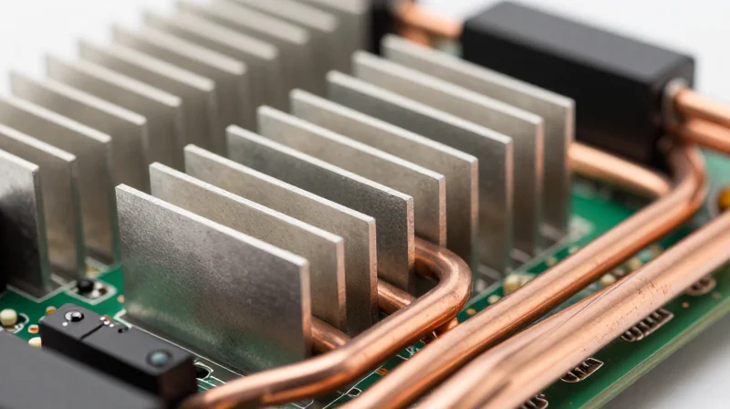
Mitigating Lifecycle Costs Through Thermal Integrity
In high-density optical transceiver PCBA designs, thermal management is not merely an engineering requirement but a primary driver of financial efficiency. When heat is poorly managed, local hotspots accelerate the degradation of delicate laser diodes and sensitive silicon-photonics interfaces. By implementing advanced thermal dissipation strategies—such as optimized copper pouring, high-conductivity thermal interface materials (TIM), and intelligent component placement—manufacturers can significantly extend the Mean Time Between Failures (MTBF). This reduction in infant mortality and mid-cycle failures translates directly into lower warranty provision requirements and minimized field service overhead, protecting the overall project ROI.
Thermal Strategy Impact Analysis
| Thermal Strategy | Cost Impact | Performance Benefit |
|---|---|---|
| Standard Passive Cooling | Low Initial/High Long-term | Risk of Hotspots |
| Optimized Heat Spreading | Moderate/Low Long-term | Uniform Temp/Longer Life |
| Integrated Micro-Cooling | High Initial/Negligible Long-term | Peak Performance/Zero Drift |
Frequently Asked Questions
- How does better thermal design improve ROI?
Reduced thermal stress directly correlates to lower failure rates. Fewer field returns mean lower logistics, replacement, and labor costs over the transceiver’s operational lifecycle. - Are high-end thermal materials justified for cost-sensitive markets?
Yes, when calculating the 'Total Cost of Ownership.' While advanced materials increase the Bill of Materials (BOM), the reduction in scrap rates and RMA costs typically offsets the investment within the first two years of deployment. - Does thermal management affect signal integrity?
Absolutely. High temperatures increase thermal noise and impedance shifts in high-speed circuits; maintaining a cooler, stable environment preserves signal quality, reducing the need for aggressive error correction overhead.
Case Study: Scaling Throughput While Reducing Scrap
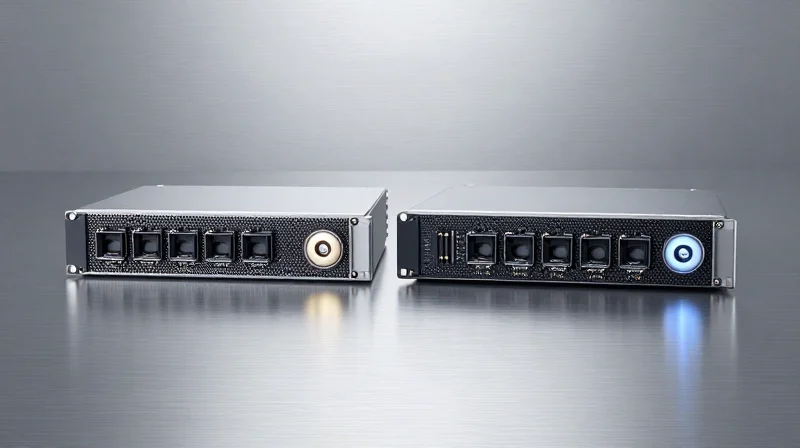
Case Study: Scaling Throughput While Reducing Scrap
A leading Tier-1 networking firm faced mounting cost pressures as their 100G and 400G optical transceiver production reached high-volume thresholds. Initially, the manufacturer struggled with a high rework rate—exceeding 8%—stemming from thermal-induced warp and SMT precision errors on high-density PCBs. By shifting to a vertical integration strategy and refined stack-up engineering, the firm successfully stabilized the assembly process, ultimately increasing total throughput by 15% and slashing scrap-related expenditures.
Performance Metrics Before and After Optimization
| Metric | Legacy Process | Optimized Process |
|---|---|---|
| First-Pass Yield | 82% | 97% |
| Scrap Rate | 8.5% | 1.2% |
| Hourly Throughput | 450 Units | 518 Units |
| Rework Labor Cost | High | Minimal |
Strategic Implementation Lessons
- How did material selection impact scrap?
The firm moved to a lower Coefficient of Thermal Expansion (CTE) substrate, which significantly mitigated PCB warpage during reflow, directly reducing component misalignment. - What role did automated optical inspection (AOI) play?
Implementing real-time AOI integration at the solder paste inspection (SPI) stage allowed for immediate process correction, preventing cascading defects that traditionally led to total board scrap. - Was there a trade-off in initial setup cost?
While the initial investment in higher-grade materials and advanced inspection equipment increased CAPEX by 12%, the ROI was realized within six months through labor savings and material recovery.
This successful transition highlights that the most effective way to maximize ROI is not through cheapening component parts, but through engineering robust stability into the PCBA assembly stack-up. By prioritizing process repeatability, the manufacturer shifted from a reactive stance on defects to a proactive model of continuous high-yield production.
The Role of Automated Inspection in Process Refinement
Closing the Loop: From Defect Detection to Process Correction
Automated Optical Inspection (AOI) and Automated X-ray Inspection (AXI) are no longer merely gatekeepers for quality control; they are essential feedback mechanisms for continuous process refinement. By capturing granular metadata on solder joint morphology, component alignment, and void ratios, manufacturers can identify the root causes of recurring deviations. This data-driven approach transitions the production line from a reactive stance—where defects are simply culled—to a proactive model, where parameters are optimized in real-time to prevent defects from manifesting.
Comparative Efficacy of Inspection Technologies
| Feature | AOI Systems | AXI Systems |
|---|---|---|
| Inspection Scope | Surface-level features, solder fillets, polarity | Internal structures, BGA joints, hidden vias |
| ROI Driver | Rapid detection of high-volume surface defects | Prevention of latent reliability failures in high-density PCBA |
| Process Impact | Optimizes placement speed and reflow thermal profiles | Refines solder paste volume and stencil design |
Strategic Implementation for Long-Term Yield Gains
Leveraging inspection data requires the implementation of a centralized quality management system (QMS) that integrates with SMT equipment. When persistent trends appear in AOI reporting—such as consistent skewing on high-density interconnects—the system should trigger automated alerts to recalibrate placement machines. This closed-loop integration is vital for optical transceivers, where even micron-level misalignments can degrade signal integrity and shorten the lifecycle of the component.
- How does automated inspection reduce long-term operational costs?
It eliminates the 'hidden factory' of rework and scrap by identifying micro-defects early in the assembly process, preventing expensive field failures. - Is AXI necessary for all optical transceiver PCBAs?
While AOI handles surface aesthetics, AXI is critical for verifying the integrity of hidden solder joints under BGA-packaged lasers and drivers, which are the most common failure points. - What is the primary barrier to effective process refinement?
The primary barrier is data siloization; inspection data must be correlated with specific lot numbers and machine settings to inform meaningful machine learning models.
Future-Proofing Your Hardware Through Integrated Design
Architecting for Long-Term Adaptability
True future-proofing in high-speed optical transceivers is achieved by decoupling the optical sub-assembly (OSA) from the primary control electronics through modular PCBA architecture. By utilizing standardized high-speed interconnects and customizable daughterboard configurations, manufacturers can transition from 100G to 400G or 800G infrastructures by swapping front-end optical engines while maintaining the core processing and power delivery backbone. This architectural approach minimizes the capital expenditure associated with full-unit replacement cycles and allows for incremental feature deployment.
| Strategy | Cost Benefit | Operational Impact |
|---|---|---|
| Modular Daughterboards | High (Component Reuse) | Accelerated Time-to-Market |
| Standardized Interconnects | Medium (Interoperability) | Simplified Supply Chain |
| Software-Defined Logic | Low (Firmware Updates) | Dynamic Performance Scaling |
Strategic Implementation Considerations
- How does modularity influence initial PCBA design costs?
While modularity requires a higher upfront NRE investment for high-precision interface design, it significantly reduces total cost of ownership by extending the service life of the base board by 3-5 years. - Can integrated designs handle future heat density requirements?
Yes, by utilizing thermal-path independent mounting systems, the PCBA can accommodate next-generation, higher-wattage optical components without violating the existing thermal envelope of the original chassis. - What is the primary risk of a modular approach?
The primary risk is signal integrity degradation at the interconnect interface; this is mitigated through rigorous simulation and the use of low-loss PCB materials specifically selected for future frequency scalability.
Ultimately, the shift toward integrated PCBA flexibility is a shift toward asset preservation. By treating the transceiver as an evolving ecosystem rather than a static component, organizations ensure that their current hardware investments remain relevant as bandwidth demands continue their aggressive upward trajectory.
Optimizing PCBA assembly is more than just a cost-saving measure; it is a fundamental shift toward sustainable, scalable hardware excellence. By focusing on design integrity and yield-centric manufacturing, companies can secure better margins and long-term reliability. Ready to optimize your hardware roadmap? Contact our engineering team today to schedule a comprehensive PCBA audit and start maximizing your ROI.
