
In the fast-paced world of electronics manufacturing, the margin for error is razor-thin. As BGA (Ball Grid Array) components continue to shrink, traditional visual inspection methods fail to detect hidden structural defects, leading to costly rework cycles and delayed time-to-market. This article explores how integrating Automated X-Ray Inspection (AXI) serves as a strategic investment to safeguard margins and enhance long-term production quality.
The Escalating Challenge of High-Density PCB Assembly

The Limitations of Optical Inspection in Modern Assembly
As component pitch shrinks and package profiles flatten, Ball Grid Array (BGA) and Chip Scale Package (CSP) components dominate modern PCB designs. These assemblies present a fundamental challenge: the solder joints are physically hidden beneath the component body. Traditional Automated Optical Inspection (AOI) relies on surface-level visual recognition, making it inherently incapable of verifying the structural integrity of these obscured joints. Relying on optical systems in a high-density environment creates a blind spot where latent defects—such as head-in-pillow, internal voids, and bridging—can bypass quality gates entirely.
Comparative Analysis: AOI vs. AXI
| Feature | Optical Inspection (AOI) | Advanced X-Ray Inspection (AXI) |
|---|---|---|
| Visibility | Surface only | Sub-surface / 3D internal |
| BGA Joint Analysis | Limited to visible edges | Full volumetric analysis |
| Defect Detection | Misalignment, polarities | Voids, bridges, head-in-pillow |
| Inspection Depth | Shallow | Deep/Transmissive |
Risk Factors in Latent Solder Defects
Latent defects are the primary driver of field failures in high-density electronics. Unlike catastrophic failures that trigger immediate test failure, latent solder joints may pass initial electrical functional tests while harboring structural weaknesses. Over time, thermal cycling and vibration induce mechanical stress, causing these compromised joints to fail, leading to costly product recalls and loss of brand reliability.
- Why are voids so dangerous in BGA assembly?
Voids reduce the effective cross-sectional area of the solder joint, significantly lowering thermal conductivity and mechanical strength, which accelerates fatigue during operational use. - What makes 'Head-in-Pillow' difficult to detect?
The solder ball and the pad touch physically but fail to coalesce, often appearing electrically sound during initial ICT (In-Circuit Testing) but separating under minor mechanical stress. - How does miniaturization impact ROI?
As component density increases, the cost of rework or field failure exponentially outweighs the capital investment required for high-resolution 3D AXI systems.
Understanding Automated X-Ray Inspection (AXI) Technology
The Physics of Subsurface Defect Detection
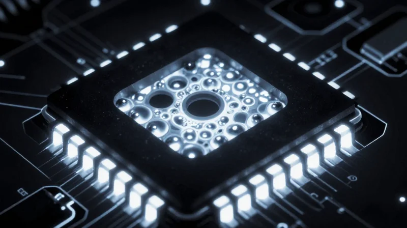
AXI technology overcomes the opacity of BGA housings by utilizing ionizing radiation to penetrate the device substrate and solder matrix. Unlike optical inspection, which is limited to the peripheral solder fillet, AXI captures the structural integrity of individual ball grid array joints by measuring the differential absorption of X-rays based on material density and atomic weight. This allows for the precise identification of voids, bridging, and insufficient wetting that remain hidden beneath the component body.
2D vs. 3D AXI Capabilities
| Feature | 2D AXI (Transmission) | 3D AXI (CT/Laminography) |
|---|---|---|
| Imaging Depth | Projected 2D shadowgraph | Cross-sectional slice reconstruction |
| Defect Clarity | Overlapping layers create noise | Eliminates overlap/distortion |
| Application | High-throughput screening | Complex multi-layer fine-pitch BGA |
3D AXI, specifically through Computed Tomography (CT) or digital laminography, provides a distinct advantage in high-density assemblies. By capturing multiple projections and reconstructing them into 3D voxels, the system can isolate a specific layer of the BGA, effectively removing the 'noise' from components located on the opposite side of the PCB.
Frequently Asked Questions
- How does AXI differentiate between a void and a micro-pore?
AXI systems use gray-scale thresholding and volumetric analysis to quantify the size and distribution of voids, allowing manufacturers to distinguish between critical structural voids and acceptable process-related porosity. - Can AXI detect 'Head-in-Pillow' (HiP) defects?
Yes, high-resolution 3D AXI is highly effective at identifying HiP defects by visualizing the vertical separation or lack of metallurgical bonding between the solder ball and the pad, which is otherwise undetectable. - Does the radiation dosage pose a risk to components?
Modern high-resolution AXI systems are designed with controlled emission parameters that ensure the radiation dose remains well below the threshold that would cause logic errors or degradation in sensitive CMOS or memory components.
Case Study: Achieving Near-Zero Latent Defects
Implementation Case Study: High-Density Telecommunications Module
A Tier-1 telecommunications hardware manufacturer faced significant yield instability when transitioning to ultra-fine pitch BGA packages. Despite rigorous Automated Optical Inspection (AOI), latent solder joint defects were escaping the production line, resulting in intermittent connectivity issues after thermal cycling in the field. By integrating advanced 3D AXI into their post-reflow process, the facility was able to detect non-visible structural anomalies, such as head-in-pillow (HiP) defects and excessive voiding, which had previously remained undetected.
Performance Comparison: Pre- vs. Post-AXI Integration
| Metric | Legacy AOI Baseline | 3D AXI Integrated |
|---|---|---|
| First Pass Yield | 84.2% | 98.7% |
| Field Failure Rate | 2.4% | 0.1% |
| Scrap Rate | 5.1% | 0.8% |
| Detection of HiP Defects | Negligible | 99.2% |
Key Lessons in Latent Defect Mitigation
- Why did previous inspection methods fail to catch latent defects?
AOI is limited to the surface level; it cannot inspect beneath the BGA package where internal solder wetting issues and head-in-pillow joints occur. - How did 3D AXI impact the overall ROI?
By shifting from reactive field repairs to proactive detection, the company saved approximately $1.2M annually in warranty claims and reduced rework labor hours by 65%. - What was the most critical factor for success?
The correlation of X-ray data back to the SPI (Solder Paste Inspection) machines allowed for real-time process adjustments, preventing systematic defects before they could propagate.
The successful deployment demonstrates that AXI is not merely a quality gate, but a fundamental process control tool. By leveraging volumetric data to refine thermal profiles and stencil designs, the manufacturer transformed their assembly line from a reactive environment into a precision-driven operation capable of achieving near-zero latent defect rates.
Direct Economic Impact: Reducing Rework and Scrap Costs
The Cost Economics of Defect Detection
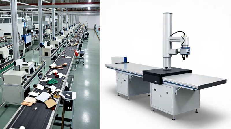
In high-density BGA assembly, the 'Rule of Tens' is the primary economic driver for ROI: the cost to detect and repair a defect increases tenfold at every stage of the manufacturing process. Identifying a hidden BGA solder void during the SMT process costs mere cents in machine time and operator intervention. Conversely, finding that same fault after the board is integrated into a finished product requires costly rework, shipping, and potential warranty claims that can erode entire profit margins.
Comparative Cost Analysis: Detection Stages
| Detection Stage | Cost Multiplier | Primary Economic Impact |
|---|---|---|
| In-Line SMT (AXI) | 1x | Low; minimal labor and scrap. |
| In-Circuit Testing (ICT) | 10x | Moderate; board rework and re-test. |
| Functional System Test | 100x | High; logistics and replacement. |
| Field/Warranty Return | 1000x | Critical; brand reputation and recall. |
Quantifying Scrap and Rework Reduction
By implementing 3D AXI, manufacturers transition from reactive end-of-line triage to proactive process control. Real-time feedback loops allow for immediate adjustments to reflow profiles and solder paste deposition, effectively cutting scrap rates by preventing the creation of defects in the first place.
- How does AXI directly reduce scrap costs?
AXI identifies process drift, such as insufficient solder volume or poor alignment, allowing operators to correct the SMT line before an entire batch of boards is compromised. - Why is rework cheaper with AXI integration?
Early detection allows for targeted, localized rework at the component level before expensive downstream components or structural housings are added to the PCB. - What is the ROI impact of eliminating latent defects?
Reducing latent defects minimizes 'no-fault-found' (NFF) returns and warranty overhead, which are often the most significant hidden expenses in electronics manufacturing.
Accelerating Time-to-Market Through Data-Driven Insights

The Closed-Loop Feedback Mechanism
Traditional SMT troubleshooting relies on manual inspection and delayed failure data, which prolongs the stabilization of high-density BGA assembly processes. Advanced AXI systems transform inspection from a 'gatekeeper' function into a 'process intelligence' engine. By automatically extracting volumetric and voiding data from every board, these systems feed precise metrics directly back into the CAD and reflow profile software. This allows process engineers to correlate specific defects—such as head-in-pillow or insufficient solder—with thermal profiles or stencil aperture geometry, enabling rapid, data-backed adjustments without the need for multiple trial-and-error manufacturing iterations.
Optimizing Reflow and Stencil Parameters
| Parameter | Common Defect | AXI-Driven Correction |
|---|---|---|
| Reflow Soak Zone | Voiding in BGA joints | Adjust soak time based on volumetric flux outgassing data |
| Stencil Aperture | Solder bridging | Reduce stencil area ratio based on measured solder volume |
| Reflow Peak Temp | Head-in-Pillow | Extend time-above-liquidus based on joint coalescence analysis |
Frequently Asked Questions on Data-Driven Optimization
- How does AXI data reduce the need for physical pilot runs?
AXI provides high-fidelity measurements on solder joint geometry and void percentages, allowing engineers to validate process changes on the first production run rather than relying on qualitative visual inspection. - Can AXI software integrate directly with Industry 4.0 MES platforms?
Yes, modern AXI systems export defect trend data via standard protocols like IPC-CFX, which enables automated decision-making and real-time adjustment of printer and oven parameters. - Does real-time feedback hinder production throughput?
Advanced AXI systems utilize AI-driven algorithms to perform inspection in parallel with the assembly line, ensuring that data-driven insights are captured without interrupting the tact time.
Integrating AXI into Your Existing SMT Line

Strategic Integration Workflow
Integrating AXI into a mature SMT line is not merely a hardware installation; it is a process re-engineering project. To maximize ROI, AXI systems should be positioned immediately post-reflow. This placement minimizes the 'cost of quality' by identifying hidden solder defects in BGA and QFN components before they propagate through the assembly process or reach final functional test stations.
Balancing Throughput with Inspection Depth
| Inspection Strategy | Throughput Impact | Detection Capability | Best Use Case |
|---|---|---|---|
| Full 3D Computed Tomography | Low | Maximum (Voiding & Head-in-Pillow) | NPI and Prototypes |
| Hybrid/Selective Inspection | Medium | High (Critical Joints) | High-Mix Production |
| 2.5D Automated Slice | High | Moderate (Bridge & Alignment) | High-Volume Mature Lines |
Implementation Best Practices and FAQ
- How do we prevent AXI from becoming a line bottleneck?
Utilize 'skip-rate' inspection logic, where only a statistical sample of boards is subjected to full 3D inspection, while 100% of boards undergo high-speed 2.5D slice inspection. - Should AXI data be linked to the MES?
Yes. Integrating AXI into your Manufacturing Execution System (MES) is critical for real-time traceability, allowing for automated feedback loops that trigger printer or pick-and-place adjustments when recurring voiding patterns are detected. - What is the primary challenge during the commissioning phase?
The greatest challenge is 'false call' calibration. Invest time in refining your Golden Board library to ensure the AXI algorithm distinguishes between acceptable process variation and genuine defects.
By following a phased integration approach—starting with high-criticality component monitoring and scaling toward full-board volumetric analysis—manufacturers can harmonize the AXI inspection cycle time with existing line takt times without sacrificing production velocity.
The Role of AI and Machine Learning in Modern Inspection
Moving Beyond Rule-Based Inspection
Traditional Automated X-Ray Inspection (AXI) systems rely on rigid, rule-based algorithms that struggle with the complexity of high-density BGA designs. As component pitches shrink and thermal management features like large ground planes create image noise, traditional systems often flag 'false calls'—identifying legitimate design features as defects. AI and Machine Learning (ML) overcome this by moving from static logic to pattern recognition, allowing the system to learn the nuances of a 'good' versus 'bad' solder joint through thousands of iterations.
Impact on Inspection Accuracy and Operational Efficiency
| Feature | Rule-Based Inspection | AI-Enhanced Inspection |
|---|---|---|
| Detection Logic | Static Thresholds | Neural Network Pattern Analysis |
| False Call Rates | High (Requires Human Review) | Low (Automated Filtering) |
| Process Adaptation | Manual Tuning Required | Self-Learning Feedback Loop |
Key Advantages for High-Density Assembly
- Reduction of Operator Fatigue
AI-driven image segmentation automatically ignores non-critical artifacts, drastically reducing the number of images an operator must manually verify. - Adaptive Thresholding
AI algorithms adjust sensitivity based on real-time process variances, ensuring consistent quality levels even as solder paste viscosity or stencil performance shifts throughout the production shift. - Predictive Defect Modeling
By analyzing subtle trends in image data, ML models can predict potential bridging or voiding issues before they exceed tolerance levels, enabling proactive process adjustments.
Strategic Implementation Considerations
Implementing AI in an AXI workflow requires a robust data strategy. For high-density BGA assembly, the system needs a diverse 'training set' of images representing both minor process drifts and actual failures. By integrating these AI-powered modules into the SMT feedback loop, manufacturers gain an autonomous quality assurance layer that continuously matures, ensuring the highest possible ROI by preventing the rework and scrap costs associated with late-stage failure detection.
Long-Term Reliability and Brand Reputation
Ensuring Field Reliability in High-Density Assemblies
In high-density BGA assembly, hidden defects such as micro-voids and head-in-pillow (HiP) fractures pose existential risks to long-term product durability. Advanced X-ray inspection goes beyond mere binary pass/fail results; it provides the granular data necessary to validate the structural integrity of solder joints under thermal and mechanical stress. By identifying latent defects early, manufacturers prevent costly field failures, reducing warranty claims and protecting the long-term operational lifespan of the end product.
Impact of AXI on Brand Equity
Brand reputation is inextricably linked to consistent quality. In sectors like medical devices, automotive electronics, and aerospace, the cost of a single component failure far exceeds the investment in advanced inspection technology. Deploying AXI signals a commitment to zero-defect manufacturing, which serves as a significant competitive differentiator. When customers know that every BGA connection has undergone 3D volumetric analysis, trust in the brand’s reliability profile increases, often leading to deeper long-term partnerships and preferred-supplier status.
| Metric | Reactive Inspection | Advanced AXI Integration |
|---|---|---|
| Field Failure Rate | Variable/Higher | Minimized/Predictable |
| Customer Trust | Transactional | Strategic Partnership |
| Warranty Liability | Significant Cost | Managed & Reduced |
| Quality Perception | Reactive | Proactive/Elite |
Common Questions on Reliability and AXI
- How does AXI reduce long-term warranty costs?
By detecting intermittent or non-apparent defects like internal voiding that standard optical inspection misses, AXI prevents flawed units from reaching the consumer, effectively eliminating the costs associated with recalls and field repairs. - Is the investment in AXI justified for all PCB assembly?
For high-density BGA packages where manual or 2D inspection is insufficient, AXI is not just an expense but an insurance policy against the catastrophic brand damage caused by high-profile field failures. - Does AXI data help improve future product designs?
Yes. Engineers can use the structural data from X-ray scans to refine footprint and thermal relief patterns, ensuring that future design iterations are inherently more robust and easier to solder reliably.
By transitioning from manual or optical-only inspection to high-precision Automated X-Ray Inspection, manufacturers can effectively mitigate the risks associated with modern BGA complexity. The resulting reduction in rework and improved throughput are not just operational wins—they are essential components of a competitive manufacturing strategy. Contact our engineering team today for a consultation on how AXI can optimize your production yield and secure your bottom line.
