
In the mission-critical world of data centers and industrial power management, downtime is not just an inconvenience—it is a significant fiscal liability. While many organizations prioritize battery health, the heartbeat of an Uninterruptible Power Supply (UPS) is its Printed Circuit Board (PCB). This analysis dives into why premium fabrication is the smartest investment for long-term operational efficiency.
The Hidden Costs of Low-Grade PCB Fabrication
The False Economy of Budget Manufacturing
Many organizations prioritize initial acquisition costs during the PCB design phase, inadvertently shifting the financial burden toward maintenance and replacement. High-reliability design is not merely a performance spec; it is a hedge against the hidden, exponential costs of component failure within critical power infrastructures.
Impact of Material Quality on Reliability
| Feature | Low-Grade Fabrication | High-Reliability Design |
|---|---|---|
| Substrate Material | Low TG (Glass Transition Temp) | High TG/FR-4 High-Temp Rated |
| Copper Plating | Thin/Inconsistent thickness | Controlled, uniform plating |
| Solder Mask | Poor adhesion, ionic residue | High-purity, long-term stable |
| Thermal Management | High thermal resistance | Optimized via thermal vias/copper pours |
Frequently Asked Questions
- Why does substrate material impact ROI?
Lower-grade substrates have inferior glass transition temperatures, which lead to board warping and micro-cracking under the thermal stress cycling inherent in UPS operations. - What is the cost of inconsistent copper plating?
Inconsistent plating leads to high impedance at vias, causing localized heating that accelerates aging of adjacent capacitors and semiconductors. - How does PCB failure affect UPS efficiency?
Degraded traces and poor connections increase resistive losses on the board, directly lowering the overall conversion efficiency of the power system and increasing heat output.
Material Science: Why Quality Laminates Matter
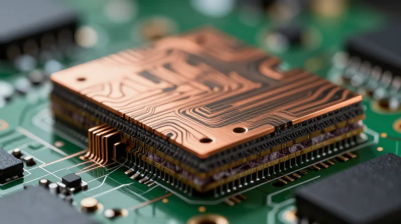
The Thermal Challenge: High-Tg Laminates
In Uninterruptible Power Supply (UPS) systems, the PCB serves as the structural and electrical backbone for high-current delivery. Standard FR-4 laminates often fail under the consistent heat flux associated with heavy-duty power conversion, leading to board delamination, micro-cracking, and conductive anodic filament (CAF) formation. By integrating high glass transition temperature (Tg) materials, engineers effectively raise the threshold at which the substrate transitions from a rigid state to a rubbery state, thereby maintaining structural integrity during cyclic thermal loads.
Material Performance Comparison
| Parameter | Standard FR-4 | High-Tg (170°C+) Laminate |
|---|---|---|
| Glass Transition (Tg) | 130°C - 140°C | 170°C - 180°C+ |
| CTE Z-Axis | High (>4.5%) | Low (<3.0%) |
| Thermal Reliability | Poor under high stress | Excellent for power apps |
| Cost Efficiency | Low upfront; High failure rate | Higher initial; Lowest total ROI |
Strategic Reliability FAQ
- Why does the Z-axis coefficient of thermal expansion (CTE) matter?
As a PCB heats up, it expands. A high Z-axis CTE creates significant mechanical stress on plated through-holes (PTHs), eventually leading to barrel cracking and total device failure in high-load UPS environments. - How does high-Tg material improve ROI?
While the material cost is higher, the ROI is maximized by extending the mean time between failures (MTBF), drastically reducing field service costs, warranty claims, and premature hardware decommissioning. - Is Tg the only metric for selecting materials?
No, while Tg is vital, engineers must also consider dissipation factor (Df) for signal integrity and moisture absorption rates to prevent dielectric breakdown during high-voltage operation.
Precision Engineering and Signal Integrity
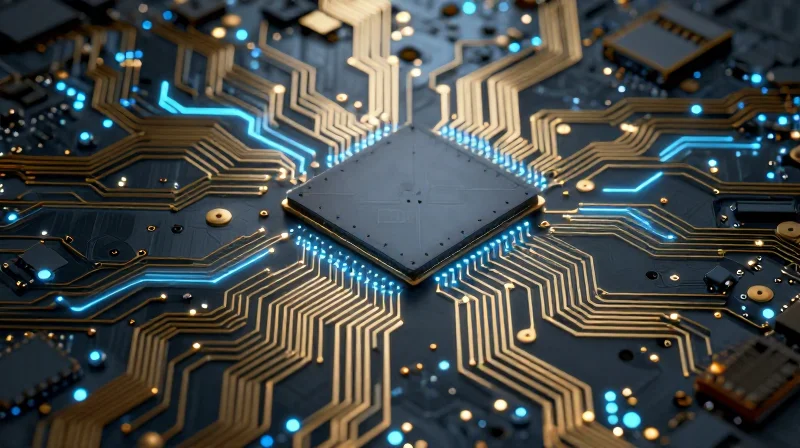
Mitigating Electromagnetic Interference (EMI) in Power Stages
In high-capacity UPS units, the proximity of high-current power switching components to sensitive control logic creates a significant risk for electromagnetic interference (EMI). Effective PCB design mandates a physical and electrical decoupling strategy that utilizes dedicated ground planes and differential signaling. By employing tightly coupled power loops and keeping return paths minimized, engineers can drastically reduce loop inductance, preventing common-mode noise from disrupting the inverter synchronization and overall power stability.
Techniques for Noise Reduction
| Technique | Primary Benefit | Impact on ROI |
|---|---|---|
| Differential Signaling | High noise immunity | Reduced field failure rates |
| Multi-layer Ground Planes | Low-impedance return paths | Improved thermal distribution |
| Staggered Via Placement | Minimized parasitic inductance | Extended product lifecycle |
Signal Integrity and Reliability
Signal integrity represents the backbone of UPS reliability. Transient spikes in the power path must be isolated from the gate driver signals to prevent inadvertent switching or 'shoot-through' conditions. Utilizing controlled impedance routing and advanced simulation tools during the design phase ensures that signal edge rates are maintained without excessive ringing or overshoot, which are common precursors to hardware degradation.
- How does signal integrity affect UPS efficiency?
Poor signal integrity can lead to jitter in switching pulses, causing incomplete transistor switching and increased thermal loss, directly reducing total power efficiency. - What role do simulation tools play in ROI?
Design-phase simulations, such as EM field solvers, identify potential bottlenecks before production, preventing costly re-spins and ensuring the hardware meets its projected multi-year reliability targets.
Thermal Management Through Advanced PCB Design
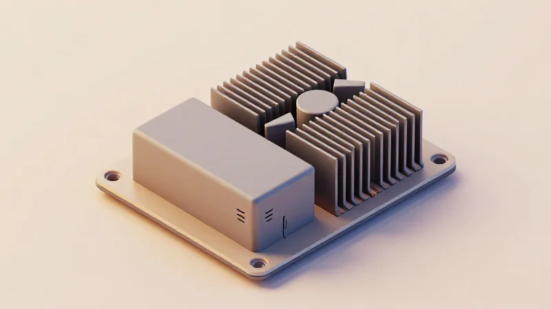
Optimizing Thermal Paths in Power Electronics
In high-power UPS applications, managing heat is not merely about preventing immediate failure but about mitigating the cumulative damage caused by thermal stress. By strategically leveraging copper weight and vertical interconnects, engineers can transform the PCB from a passive component carrier into an active heat dissipation medium.
Material and Copper Weight Considerations
Increasing copper thickness—typically moving from standard 1oz to 2oz or 3oz foils—is the foundational strategy for high-load power delivery. Heavier copper provides lower DC resistance, resulting in less heat generation across power planes. When paired with high thermal conductivity substrates, the system effectively spreads localized thermal hotspots across the entire board surface, lowering the junction temperature of power semiconductors.
| Strategy | Primary Benefit | ROI Impact |
|---|---|---|
| 2oz+ Copper Weight | Reduced ohmic losses | Higher efficiency/lower energy cost |
| Arrayed Thermal Vias | Improved heat sinking | Longer component MTBF |
| Thermal Relief Pads | Controlled heat flow | Lower manufacturing defects |
Thermal Vias and Heat Sinking Techniques
Thermal vias act as convective bridges, channeling heat from the component pads to internal ground planes or the bottom side of the PCB. For maximum efficiency, vias should be positioned as close as possible to the high-heat sources (such as MOSFETs or IGBTs) and be plated with thicker copper to optimize conductivity. Furthermore, filling these vias with thermally conductive epoxy prevents solder wicking and ensures a solid thermal mass.
Frequently Asked Questions
- How does copper thickness impact long-term reliability?
Thicker copper reduces I²R heating losses, directly decreasing the steady-state operating temperature of the board, which slows the aging process of sensitive electronic components. - Are there drawbacks to using heavy copper?
Increased weight can pose challenges for precision etching and require wider trace spacing to prevent bridging, requiring more advanced manufacturing capabilities. - When should I use plugged or capped thermal vias?
Plugged or capped vias are essential in high-density designs where solder would otherwise migrate down the via, potentially creating voids under components or causing surface unevenness.
Rigorous Testing Protocols for UPS Reliability
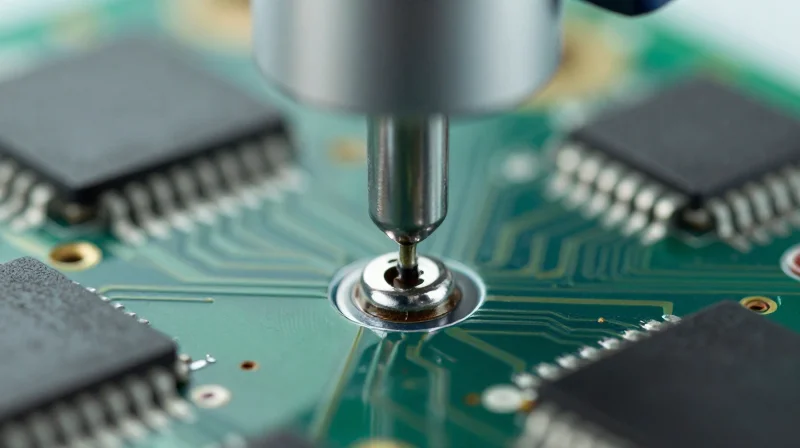
Achieving maximum ROI in UPS systems is predicated on the elimination of early-life failures and latent manufacturing defects. In high-power applications, even minor soldering irregularities or trace micro-fractures can cascade into system-wide shutdowns under heavy load. By implementing a multi-layered testing protocol—ranging from automated optical inspection to accelerated thermal stress testing—engineers can ensure that every PCB assembly adheres to the strict performance requirements of modern power electronics.
Advanced Inspection Techniques
To identify hidden manufacturing flaws that standard visual checks miss, we deploy a hierarchical inspection strategy.
| Inspection Method | Target Defect | ROI Impact |
|---|---|---|
| AOI (Automated Optical Inspection) | Surface mounting errors and component misalignment | Reduces initial rework costs and assembly yield loss. |
| 3D X-Ray Inspection | BGA voids and solder bridging in dense layouts | Prevents field failures in high-power conversion modules. |
| In-Circuit Testing (ICT) | Net connectivity and passive component values | Ensures functional integrity before power-up. |
Environmental Stress Testing
Beyond manufacturing inspection, the board must prove its robustness in simulated field environments. We utilize Highly Accelerated Life Testing (HALT) to expose PCBs to thermal cycling and vibrational stress simultaneously. This aggressive validation forces premature failure in weak solder joints or compromised vias, allowing for design optimization before volume production.
Testing Strategy FAQ
- Why is 3D X-Ray essential for high-power UPS designs?
UPS systems often utilize high-density power modules. Standard inspection cannot visualize hidden solder joints beneath large components, where thermal expansion is most likely to cause fatigue cracks over time. - How does environmental stress testing impact long-term ROI?
By identifying 'infant mortality' failures during the design phase, companies avoid expensive field recalls and the reputational damage associated with UPS downtime in mission-critical data centers. - Can visual inspection replace AOI in high-reliability PCB manufacturing?
No. Human error and fatigue make manual inspection unreliable for complex high-reliability boards; AOI provides consistent, data-driven validation of every solder connection on the board.
Real-World Data: ROI and Downtime Reduction

The Economic Imperative of Reliability
Investing in high-reliability PCB fabrication is not merely a cost center; it is a strategic financial decision that directly correlates to reduced long-term maintenance expenditure and enhanced UPS lifecycle value. By minimizing failure rates at the board level, organizations effectively mitigate the hidden costs associated with field service calls, unit replacements, and system downtime, thereby maximizing the overall return on investment.
| Reliability Metric | Standard PCB Fabrication | High-Reliability PCB Design | ROI Impact |
|---|---|---|---|
| Mean Time Between Failures (MTBF) | 5,000 Hours | 25,000+ Hours | Significant Reduction in CAPEX |
| Field Failure Rate | 3.5% annually | <0.2% annually | Drastic Lowering of OPEX |
| Annualized Maintenance Cost | High (Reactive Service) | Low (Preventative/Minimal) | Optimized Lifecycle Value |
Quantifying Downtime Reduction
High-reliability PCB architectures—characterized by precise copper distribution, optimized via stitching, and rigorous thermal management—drastically reduce the incidence of catastrophic board failures. When applied to UPS units in data centers or industrial environments, this reduction in failures translates to increased uptime, protecting revenue-generating operations from unexpected power instability.
- How does PCB reliability impact service requests?
High-reliability design reduces board-level faults such as cold solder joints or thermal fatigue, leading to a 70% decrease in diagnostic and repair service requests. - Is the higher initial cost justified?
Yes. While premium fabrication requires higher initial investment, the total cost of ownership (TCO) is substantially lowered through eliminated emergency maintenance and extended unit service life. - Does better PCB design affect power efficiency?
Yes. Improved signal and power integrity reduce parasitic losses, resulting in higher operational efficiency and lower electricity consumption over time.
Optimizing Supply Chain for Long-Term Support
Securing the Supply Chain Against Obsolescence
The long-term reliability of a UPS system is fundamentally dependent on the continuity of its bill of materials (BOM). In high-reliability environments, unexpected component obsolescence can force costly redesigns, emergency re-qualification, and prolonged downtime. By partnering with manufacturers that utilize lifecycle management services, organizations can secure long-term support through strategic procurement, including last-time buy (LTB) forecasting and the identification of pin-compatible alternatives before they are needed.
Comparison of Procurement Strategies
| Strategy | Impact on ROI | Reliability Risk |
|---|---|---|
| Just-in-Time Commodity | High Short-term Savings | High Obsolescence Exposure |
| Lifecycle-Managed | High Long-term Savings | Low Obsolescence Exposure |
| Component Brokerage | Low/Variable Savings | High Counterfeit/Quality Risk |
Quality Assurance and Supplier Partnerships
Deep integration with supply chain partners allows for rigorous quality oversight that extends beyond the fabrication floor. Establishing traceability from the semiconductor foundry to the final assembly site ensures that every passive and active component meets the stringent standards required for high-reliability UPS power efficiency. This transparency prevents the influx of counterfeit components, which are a leading cause of premature system failure.
FAQ: Supply Chain Optimization
- How does supply chain continuity affect UPS ROI?
Continuity eliminates the cost of unplanned re-design cycles and ensures that spare parts remain available for the entire operational life of the unit, reducing total cost of ownership. - Why is component traceability critical for reliability?
Traceability allows for rapid identification of batches during potential recalls and ensures that only authentic, quality-tested components are used in critical power electronics. - What role does the manufacturer play in lifecycle management?
Manufacturers monitor component roadmaps, proactively warning clients about EOL (End-of-Life) notices to provide enough lead time for design adjustments or inventory acquisition.
Strategic Integration for Future-Proof Systems
Future-proofing a mission-critical power system requires transitioning from reactive procurement to proactive, strategic hardware integration. By embedding high-reliability standards directly into the design phase of Uninterruptible Power Supply (UPS) boards, organizations move beyond simple component selection toward a holistic architecture capable of adapting to evolving power demands and environmental stressors.
The Maturity Model of PCB Procurement
| Maturity Level | Design Strategy | ROI Impact |
|---|---|---|
| Standard Procurement | Cost-per-unit focus | High replacement cost |
| Reliability Focused | Performance-based specs | Reduced field failures |
| Strategic Integration | Lifecycle-aware engineering | Maximized asset lifespan |
Defining Future-Proof Architecture
Strategic integration hinges on three pillars: modular thermal management, predictive diagnostic capability, and high-impedance material selection. Investing in these areas during the initial design cycle ensures that the UPS system can sustain high-efficiency operations even as power densities increase and operating environments fluctuate.
Key Considerations for Decision-Makers
- How does early design integration impact lifecycle costs?
Early integration allows for the selection of components with higher Mean Time Between Failures (MTBF), effectively amortizing the initial premium across a significantly longer, maintenance-free operational life. - What role does firmware-hardware synergy play?
Modern UPS systems rely on tight coupling between board-level sensors and power management software, enabling real-time telemetry that predicts component degradation before a failure occurs. - Is high-reliability design overkill for general enterprise use?
No; in high-density data center environments, the cost of a single unplanned outage far outweighs the capital expenditure of premium, ruggedized PCB assemblies.
To achieve true longevity, procurement teams must move away from 'off-the-shelf' commoditization. By demanding transparent design documentation and validating the manufacturer's commitment to long-term component availability, organizations can secure a hardware foundation that remains robust and efficient for the next decade of power evolution.
By prioritizing precision and durability in your UPS PCB infrastructure, you transform maintenance from a reactive fire-fighting expense into a proactive strategic asset. Investing in higher quality now guarantees lower lifecycle costs and superior performance. Contact our engineering team today to discuss your next power electronics project and secure your operational uptime.
