
In the high-stakes environment of modern data centers, the smallest discrepancy in PCB performance can cascade into massive operational failures. As data rates climb, traditional manufacturing approaches are no longer sufficient. This article explores how engineering-led design and advanced fabrication techniques safeguard signal integrity and transform your hardware's total cost of ownership.
The Direct Correlation Between PCB Design and Switch Performance
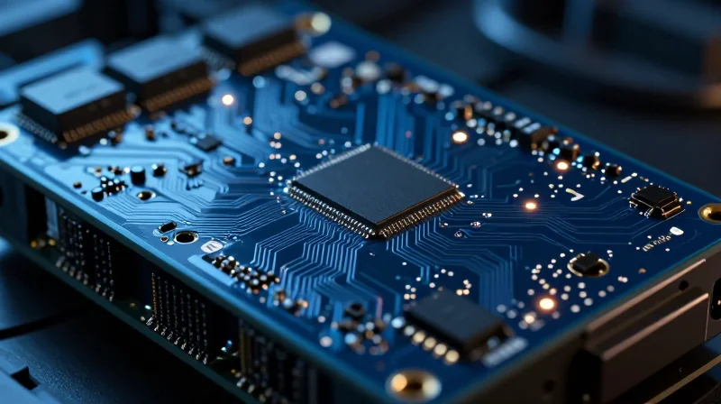
In the context of next-generation data center switch architecture, the printed circuit board (PCB) is far more than a mounting substrate; it is a critical high-frequency transmission medium. As port densities increase and data rates push toward 800G and beyond, the PCB becomes the primary bottleneck for signal integrity. Precise control over trace geometry, dielectric constant consistency, and layer-to-layer registration is required to minimize insertion loss and crosstalk. When these parameters are optimized at the manufacturing stage, the switch achieves lower latency and reduced packet loss, effectively extending the product's operational lifespan and maximizing return on investment.
Signal Integrity vs. Manufacturing Precision
At speeds exceeding 100Gbps per lane, PCB manufacturing tolerances become exponentially more demanding. Minor variations in copper foil roughness or laminate resin content can induce jitter and signal attenuation. Engineers must balance high-performance materials—such as ultra-low-loss laminates—with manufacturing techniques that ensure impedance control across the entire switch fabric. The following table highlights how specific manufacturing attributes correlate to switch performance metrics.
| Manufacturing Variable | Performance Impact | ROI Driver |
|---|---|---|
| Copper Roughness | Skin effect loss | Extended reach, reduced repeaters |
| Dielectric Consistency | Phase jitter | Reduced bit error rates (BER) |
| Via Stub Length | Return loss | Higher signal bandwidth |
Key Considerations for Switch Designers
- How does PCB material selection influence switch longevity?
Using high-glass-transition temperature (Tg) materials prevents thermal fatigue during constant high-load operations, ensuring the switch maintains stable performance over a longer multi-year deployment cycle. - What is the role of back-drilling in high-speed switches?
Back-drilling removes non-functional via stubs that act as antennas, significantly reducing signal reflection and enabling cleaner high-speed data transmission through the internal layers of the board. - Why is layer registration critical for high-density interconnects?
Poor layer registration causes impedance mismatches at signal vias, which can lead to catastrophic data loss at high frequencies, effectively nullifying the potential of high-end ASIC components.
Mitigating Signal Loss through Material Selection and Stack-up Design
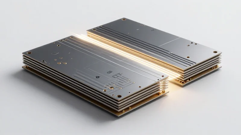
Overcoming Signal Attenuation with Low-Loss Dielectrics
As switch architectures shift toward 800G and beyond, traditional FR-4 materials become insufficient due to excessive dielectric loss (Df). To maintain signal integrity across high-speed SerDes links, engineers must transition to advanced low-loss and ultra-low-loss laminates that minimize energy dissipation at high frequencies.
| Material Grade | Typical Df (10 GHz) | Application Suitability |
|---|---|---|
| Standard FR-4 | 0.015 - 0.020 | Legacy 10G/25G interfaces |
| Low-Loss Laminate | 0.005 - 0.008 | 100G/200G standard switches |
| Ultra-Low-Loss PTFE/Ceramic | < 0.003 | 400G/800G+ data center backplanes |
Optimizing Layer Stack-up for Impedance Control
Effective stack-up design is the primary defense against electromagnetic interference (EMI) and impedance discontinuities. By utilizing symmetrical layer builds and incorporating precise copper roughness management, designers can significantly extend the reach of high-speed signals before requiring active retimers or costly signal conditioning components.
Technical Considerations for Stack-up Optimization
- How does copper profile affect insertion loss?
Lower copper roughness profiles reduce the 'skin effect' at high frequencies, significantly decreasing conductor losses which become dominant as data rates climb above 56 Gbps. - What is the benefit of back-drilling via stubs?
Removing unused via stubs eliminates resonant frequency reflections that manifest as signal suck-outs, ensuring a clean eye diagram for multi-gigabit data channels. - How do board thickness and layer count impact ROI?
While thinner boards with more layers increase raw material costs, they allow for shorter signal paths and better ground plane coupling, reducing the need for expensive signal repeaters and long-term maintenance.
Leveraging Advanced Fabrication Techniques for Signal Integrity
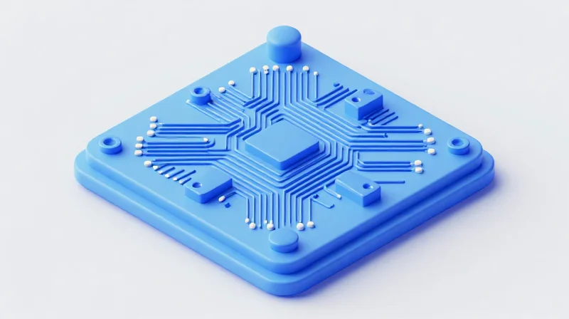
Precision Copper Etching and Trace Geometry
At frequencies exceeding 112Gbps per lane, trace geometry is not merely a design constraint but a critical variable in impedance control. Advanced fabrication processes utilize laser-direct imaging (LDI) and modified semi-additive processes (mSAP) to achieve superior etch factors. By reducing the trapezoidal cross-section typical of standard etching, engineers can minimize skin effect losses and ensure that differential pairs maintain uniform impedance across the entire length of the high-speed routing.
Optimizing Signal Paths with Via-in-Pad Technology
Via stubs act as resonant antennas at high frequencies, causing significant signal reflections and insertion loss. Implementing via-in-pad with conductive epoxy filling and over-plating (VIPPO) allows for the reduction of via stub length to near-zero, effectively eliminating potential resonance points. This fabrication strategy is essential for modern switch architectures that rely on high-density ball grid array (BGA) components for multi-terabit switching fabrics.
| Fabrication Technique | Primary Benefit | Impact on ROI |
|---|---|---|
| mSAP Etching | Improved impedance control | Higher yields at 112G+ |
| VIPPO (Via-in-Pad) | Elimination of via stubs | Reduced re-spins |
| ENEPIG Finish | Broadband signal stability | Increased component longevity |
Fabrication FAQ
- Why is surface finish choice critical for 112G+ architectures?
Surface finishes influence skin effect losses. Electroless Nickel Electroless Palladium Immersion Gold (ENEPIG) provides a flat, conductive surface that minimizes high-frequency signal degradation compared to standard HASL finishes. - How does mSAP differ from traditional subtractive etching?
mSAP uses a seed layer and patterned plating, resulting in vertical sidewalls and tighter trace tolerances, which are essential for maintaining strict impedance requirements in dense data center PCBs. - Does via-in-pad increase the risk of soldering defects?
While it requires more complex manufacturing steps, properly controlled VIPPO processes prevent solder wicking and voids, ultimately increasing reliability and reducing long-term field failure costs.
Preventing Field Failures: A Deep Dive into Reliability Testing
Preventing Field Failures: A Deep Dive into Reliability Testing
In the context of next-generation switch architectures, early-life failures are often the result of latent material defects exacerbated by operational stress. By implementing a rigorous reliability testing suite, manufacturers can predict fatigue patterns before deployment, thereby safeguarding long-term ROI and reducing costly field service interventions.
Critical Stress Environments
| Test Protocol | Primary Failure Mode Addressed | Strategic Benefit |
|---|---|---|
| Thermal Cycling | Interconnect/Via Cracking | Ensures CTE compatibility under temperature swings. |
| Vibration Testing | Solder Joint Fatigue | Validates structural integrity in high-airflow cabinets. |
| Humidity Stress | Conductive Anodic Filament (CAF) | Prevents dendritic growth and shorts in humid data centers. |
Operational Reliability FAQ
- How does thermal cycling impact signal integrity?
Repetitive thermal expansion and contraction can stress plated through-holes (PTHs). Over time, these micro-cracks alter the impedance profile of the signal path, leading to intermittent bit errors. - Why is vibration testing essential for dense switch designs?
Modern high-density switches generate significant cooling airflow. Constant vibration from high-RPM fans can fatigue solder joints on heavy BGA components, necessitating robust material selection and mechanical bracing. - What is the role of Highly Accelerated Life Testing (HALT)?
HALT is used to push the board beyond its design limits to identify weak points quickly. This 'test-to-fail' methodology is crucial for surfacing latent defects in complex, high-layer-count PCB architectures.
Case Study: Achieving 30% Reduction in RMA Rates

The Challenge: Identifying Root Causes for Field Returns
Before the intervention, a tier-one network equipment provider faced an alarming increase in RMA (Return Merchandise Authorization) rates, specifically linked to intermittent connectivity failures in next-generation 400G and 800G switches. Initial investigation revealed that inconsistent via-plating reliability and thermal stress-induced micro-cracks in the PCB stack-up were the primary drivers of these field failures.
Implementing Collaborative DFM Optimization
The company shifted from a traditional 'throw-over-the-wall' design process to a collaborative DFM framework involving constant engagement between layout engineers and fabrication specialists. This pivot focused on three strategic pillars: enhanced via aspect-ratio verification, optimized copper balancing to prevent warpage, and stringent surface finish validation (ENIG vs. Immersion Silver) to suit thermal cycling requirements.
| Failure Mode | Legacy Approach | Optimized Protocol |
|---|---|---|
| Via Reliability | Standard drill & plate | Advanced drill-to-copper, laser-drilled microvias |
| Stack-up Integrity | Symmetric balancing only | Coefficient of thermal expansion (CTE) matching |
| Assembly Stress | Manual thermal inspection | Real-time stress analysis and fatigue modeling |
Lessons Learned and Operational Impact
- How does early DFM engagement impact long-term ROI?
By identifying potential structural weaknesses before fabrication, the firm saved millions in recall costs and minimized downtime for end-users, effectively paying for the design engineering overhead within the first quarter. - Why was the reduction in RMA rates so significant?
The 30% reduction was achieved by moving beyond mere compliance with industry standards to applying custom reliability margins specifically calibrated for high-density, high-thermal output switch environments. - What is the key takeaway for hardware architects?
Signal integrity cannot be managed in isolation; physical structural resilience must be the foundation of any high-frequency PCB design strategy.
Economic Impact: Maximizing ROI Through Lifecycle Management
Shifting from CAPEX-Focused Procurement to Lifecycle Value
In the context of next-generation data center switch architecture, the procurement strategy often errs on the side of low-cost upfront manufacturing. However, this myopia ignores the compounding costs of downtime, onsite maintenance, and premature hardware decommissioning. By pivoting toward a Total Cost of Ownership (TCO) model, organizations can justify premium PCB manufacturing techniques—such as advanced resin materials and rigorous copper plating consistency—as high-yield investments that directly insulate the bottom line against the volatility of field failures.
Financial Impact of Manufacturing Quality
| Manufacturing Variable | Low-Cost Approach Risk | High-Reliability Benefit |
|---|---|---|
| Material Selection | Signal loss and delamination | Extended thermal endurance |
| Via-in-pad plating | Micro-cracking under stress | Superior interconnect integrity |
| Surface Finish | Oxidation and impedance drift | Enhanced signal stability |
FAQs: Maximizing ROI in PCB Lifecycle Management
- How does PCB manufacturing quality affect switch lifespan?
High-quality manufacturing reduces latent defects that manifest as thermal fatigue during operation, effectively extending the MTBF (Mean Time Between Failures) and deferring expensive forklift hardware upgrades. - Can investment in board quality reduce operational overhead?
Yes, superior manufacturing drastically lowers the frequency of RMA requests and unscheduled maintenance visits, which are the primary drivers of inflated operational expenditure in data centers. - What is the primary ROI driver for premium PCB processes?
The ROI is primarily driven by the 'avoided cost' of field failure repairs, which includes not only the replacement hardware but also the logistics and skilled labor costs associated with data center maintenance.
Ultimately, the transition to high-density switch architectures necessitates a move away from commodity-grade PCBs. When manufacturing precision is prioritized at the design phase, the resulting hardware provides a stable, long-term foundation that allows data center operators to maximize uptime while successfully extending the depreciation cycle of their capital equipment.
Design for Manufacturing (DFM) as a Strategic Advantage
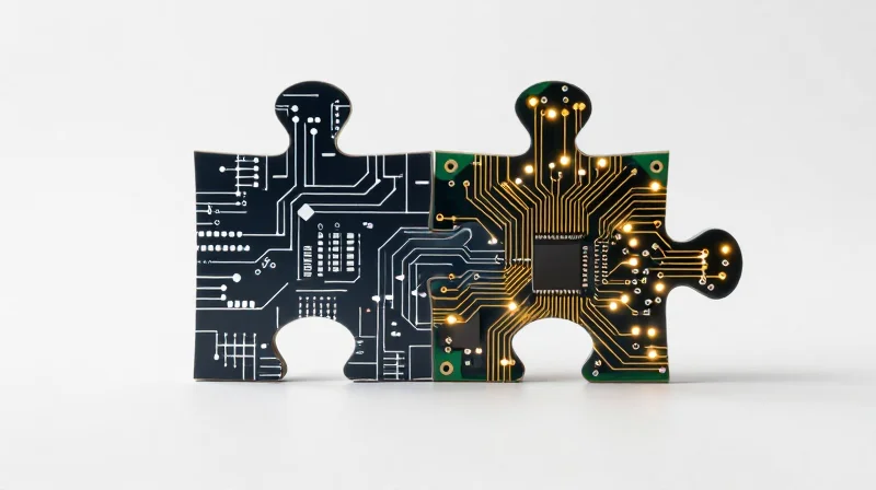
Shifting Manufacturing Intelligence to the Design Phase
In the high-speed environment of data center switch architecture, the traditional handoff between design engineers and fabrication houses is a primary source of inefficiency. By treating DFM not as a final audit but as a continuous strategic integration, organizations can identify signal integrity bottlenecks and physical assembly constraints long before the first prototype hits the production line. This proactive alignment ensures that complex, high-layer-count PCB stacks are manufacturable with standard high-yield processes, significantly reducing the financial burden of engineering change orders (ECOs).
DFM vs. Traditional Design Flow: ROI Impact
| Parameter | Traditional Design Flow | DFM-Integrated Strategy |
|---|---|---|
| Development Timeline | Extended by iterative re-spins | Accelerated via first-pass yields |
| Prototyping Costs | High due to frequent revisions | Optimized through early simulation |
| Manufacturing Reliability | Reactive to field failures | High reliability by design |
| Time-to-Market | Delayed | Market-leading |
Key DFM Considerations for High-Performance Switches
- How does early DFM impact high-speed signal integrity?
Early collaboration allows for the precise alignment of laminate selection and copper weights with specific PCB manufacturing capabilities, preventing impedance discontinuities caused by fabrication tolerances. - Can DFM reduce total cost of ownership?
Yes, by optimizing panel utilization and standardizing via geometries, DFM directly reduces scrap rates and component procurement costs, leading to lower unit prices at scale. - Why is DFM critical for complex switch architectures?
Next-gen switches require extreme density; DFM rules ensure that advanced HDI (High Density Interconnect) features, such as laser-drilled micro-vias, are within the fabricator's proven process window, eliminating yield-killing defects.
Ultimately, the strategic application of DFM creates a closed-loop system where manufacturing data informs architectural choices. This maturity in product development does more than just lower costs—it establishes a robust manufacturing baseline that allows engineering teams to focus on pushing the boundaries of switch performance rather than firefighting production errors.
Future-Proofing Your Switch Architecture
Anticipating Next-Generation Bandwidth Requirements
As data centers transition to 800G and 1.6T port speeds, PCB architectures must mitigate signal integrity degradation caused by increased insertion loss and crosstalk. Future-proofing necessitates the transition to ultra-low-loss (ULL) laminates and advanced surface finish technologies that maintain performance thresholds beyond current 112G SerDes requirements.
Strategic Material Selection for Longevity
| Parameter | Current Standard | Next-Gen Requirement |
|---|---|---|
| Dielectric Constant (Dk) | 3.4 - 3.6 | < 3.0 |
| Dissipation Factor (Df) | 0.003 - 0.004 | < 0.001 |
| Copper Profile | Standard/Low Profile | Ultra-Low/VLP |
Modular Design and Scalability Considerations
Designing for modularity—specifically disaggregated switch architectures—allows operators to upgrade switching silicon without replacing the entire chassis backplane. By leveraging blind/buried vias and back-drilling precision, engineers can extend the viability of the base PCB platform across multiple hardware refresh cycles, significantly enhancing long-term ROI.
Frequently Asked Questions
- How does PCB manufacturing impact the lifecycle of switch hardware?
Superior manufacturing processes, such as laser-drilling and high-precision impedance control, reduce thermal stress on the board, preventing delamination and extending the operational lifespan of the switch under high-load conditions. - What is the primary risk of not preparing for 800G+ architectures today?
Failure to utilize advanced low-loss materials today will result in signal degradation at higher frequencies, forcing a complete and costly board redesign when hardware requirements inevitably scale upward. - Does modular architecture increase initial manufacturing costs?
While modular designs often require higher initial investment in precision connectors and mechanical tolerances, the reduction in full-chassis replacements provides a lower total cost of ownership (TCO) over a five-year deployment window.
Optimizing PCB manufacturing is not just a technical necessity; it is a vital business strategy for any organization looking to scale its data center operations. By prioritizing signal integrity and manufacturing precision, you secure your infrastructure against premature failure and maximize ROI. Contact our engineering team today to discuss how we can elevate your hardware architecture for long-term performance.
