
In the high-stakes world of automated industrial welding, a single PCB failure can halt production lines for hours, costing manufacturers thousands in lost revenue. As power requirements grow and thermal stress becomes more acute, the traditional 'standard' circuit board design is no longer sufficient. This article explores how meticulous stack-up engineering and material selection serve as the backbone of reliable, high-performance welding systems.
The Intersection of Power Density and Thermal Reliability
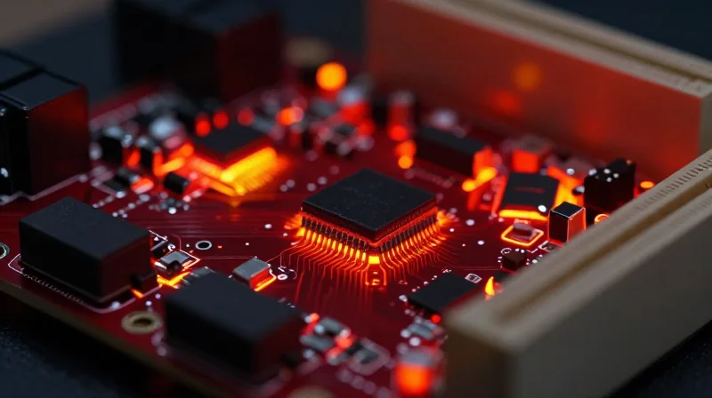
The Challenge of Thermal Flux in Welding PCBs
Automated welding systems operate at the edge of physical capability, forcing PCBs to manage massive currents that translate into significant thermal flux. When power density increases, the PCB is no longer just a structural substrate but a mission-critical thermal management component. Failure to dissipate heat at the source leads to accelerated dielectric breakdown and solder joint fatigue, ultimately shortening the operational lifespan of the entire system.
Critical Factors in Thermal Reliability
| Parameter | Design Consideration | ROI Impact |
|---|---|---|
| Current Density | Thick Copper/Inlays | Reduced energy loss/lower heat |
| Thermal Expansion | CTE-matched laminates | Extended component lifespan |
| Heat Dissipation | Thermal via stitching | Increased system uptime |
Frequently Asked Questions
- How does power density affect PCB longevity?
High power density creates concentrated heat zones that induce micro-cracks in solder joints due to constant thermal expansion and contraction, which can lead to premature system failure. - What is the role of CTE matching in welding applications?
Coefficient of Thermal Expansion (CTE) matching ensures that the board materials and surface-mount components expand at the same rate, preventing mechanical stress on connections during intense welding cycles. - Can precision manufacturing improve overall ROI?
Yes, by utilizing advanced materials and optimized layout design, precision manufacturing reduces heat-related maintenance intervals, thereby increasing the system's operational ROI over its lifecycle.
Strategic PCB Stack-up Design for Power Integrity
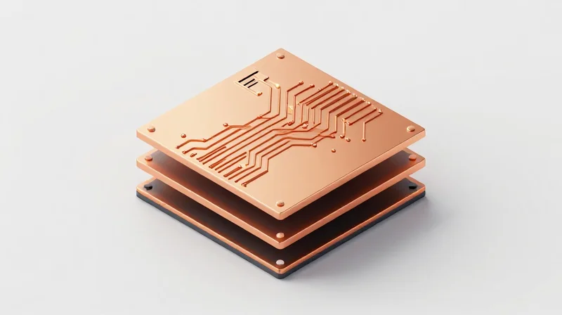
In high-power welding environments, the PCB stack-up is more than a mechanical substrate; it is a critical thermal and electrical management system. By optimizing copper weight and dielectric positioning, engineers can minimize voltage drops, reduce I2R (resistive) heating, and effectively shield sensitive control circuitry from high-energy electromagnetic interference (EMI) generated by welding arcs.
Optimizing Copper Weight and Current Capacity
Selecting the appropriate copper weight is the primary lever for minimizing heat dissipation within the conductive planes. Using heavier copper (2oz to 4oz or greater) reduces the cross-sectional resistance of the trace, which directly lowers power loss and limits thermal stress during sustained high-current operations.
| Copper Weight | Current Capacity | Recommended Application | Thermal Impact |
|---|---|---|---|
| 1 oz | Low | Control Signal Logic | High rise at high current |
| 2 oz | Medium | Secondary Power Rails | Moderate dissipation |
| 3 oz+ | High | Main Welding Current Path | Low thermal footprint |
Managing Electromagnetic Interference through Layer Geometry
To mitigate EMI in automated welding, the stack-up must utilize symmetric construction with dedicated ground planes adjacent to high-speed signal layers. Placing high-current power planes in the center of the stack-up, shielded by ground planes on top and bottom, creates an effective Faraday cage effect that prevents crosstalk and signal degradation.
Frequently Asked Questions
- How does dielectric thickness impact power integrity?
Thinner dielectrics between power and ground planes increase inter-plane capacitance, which helps stabilize voltage during rapid current switching in welding cycles. - Why is stack-up symmetry important for high-power PCBs?
Symmetry prevents mechanical warping during thermal cycling and helps balance the impedance profiles, ensuring the board remains structurally sound under extreme welding conditions. - What role do thermal vias play in stack-up design?
Thermal vias act as conduits to move heat away from surface-mount components, transferring it to internal copper planes which act as heat sinks.
Selecting High-TG Materials for Extreme Welding Environments
Selecting High-TG Materials for Extreme Welding Environments
In the context of high-power automated welding, PCBs are subjected to repetitive, extreme thermal cycles that can cause standard FR-4 laminates to expand and fracture. By specifying high-Tg materials—typically those with a Tg exceeding 170°C—manufacturers ensure the substrate maintains its mechanical rigidity and dielectric properties even as local heat spikes occur. This material selection acts as a primary defense against pad lifting, via barrel cracking, and localized delamination, effectively preserving the electrical path under high-current loads.
Material Performance Comparison
| Material Type | Typical Tg (°C) | Thermal Reliability | Recommended Use Case |
|---|---|---|---|
| Standard FR-4 | 130-140 | Low | Low-power consumer electronics |
| Mid-Tg FR-4 | 150-160 | Moderate | General industrial controllers |
| High-Tg Epoxy | 170-180+ | High | High-power welding/Automotive |
| Polyimide | 250+ | Extreme | Aerospace/High-heat military |
Technical FAQ for Material Selection
- Why does a higher Tg improve PCB ROI?
A higher Tg reduces the Coefficient of Thermal Expansion (CTE), preventing micro-fractures in copper interconnects. This minimizes costly field failures and downtime, directly maximizing the lifespan of the welding system. - What is the primary risk of using low-Tg materials in welding?
When temperatures exceed the material's Tg, the resin enters a rubbery state, leading to rapid expansion and structural failure. This frequently manifests as cracked solder joints or severed via barrels. - Does high-Tg material affect manufacturing processes?
Yes, these materials often require higher lamination temperatures and specialized drilling profiles to account for increased resin hardness, necessitating collaboration with a PCB fabricator experienced in heavy copper and high-heat applications.
Minimizing Parasitic Inductance in High-Frequency Welding

Controlling Parasitic Inductance for System Reliability
In high-frequency welding applications, parasitic inductance acts as an unintended energy storage element that triggers destructive voltage transients. When high currents are switched rapidly, any loop area within the PCB traces creates a magnetic field that resists current changes, leading to back-EMF spikes that can exceed the breakdown voltage of MOSFETs and IGBTs. Achieving optimal Return on Investment (ROI) requires mitigating these inductive losses through tight geometric coupling and minimized current loop paths.
Design Techniques for Loop Area Reduction
- Trace Geometry Optimization
Utilize wide, short traces to reduce self-inductance. Increasing the proximity of high-current paths to their respective return paths on adjacent layers minimizes the magnetic loop area. - Multi-Layer Ground Planes
Implement solid, contiguous ground planes directly beneath high-frequency switching signals to provide a low-impedance path for return currents, effectively canceling inductive fields. - Component Placement Strategy
Prioritize the physical proximity of decoupling capacitors to the switching semiconductors to form the smallest possible power loop, restricting transient noise to a localized area.
Comparison of Inductance Mitigation Strategies
| Technique | Primary Benefit | Implementation Difficulty |
|---|---|---|
| Adjacent Return Planes | Maximizes flux cancellation | Moderate |
| Vertical Via Stitching | Reduces ground loop impedance | Low |
| Embedded Capacitance | Distributes high-frequency filtering | High |
By reducing parasitic inductance, manufacturers significantly extend the service life of switching components and decrease the necessity for oversized passive filtering circuitry. This precision approach not only stabilizes the welding arc quality—leading to higher product yields—but also reduces the maintenance costs associated with premature power stage failure, directly contributing to superior long-term ROI.
Thermal Management Solutions: Vias, Heatsinks, and Thermal Pads
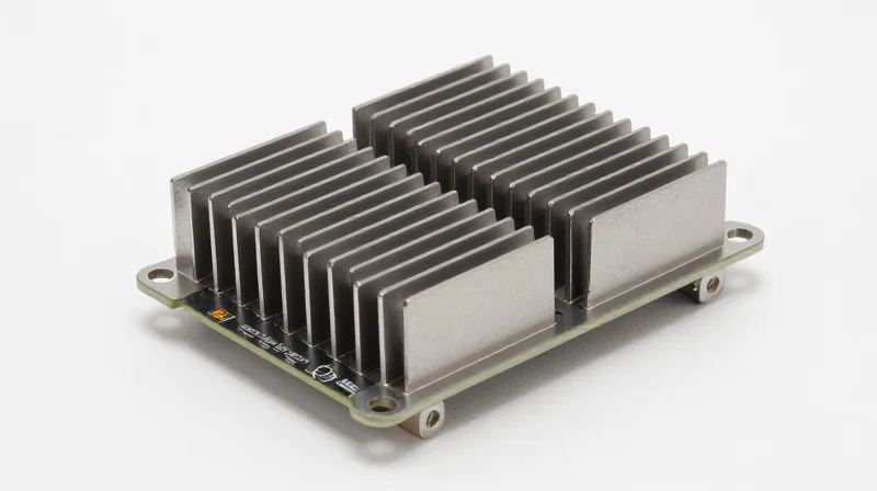
Engineered Thermal Dissipation Strategies
In advanced automated welding systems, high-current pulses generate localized heat spikes that can degrade substrate integrity and trigger premature component failure. By integrating a multi-tiered cooling approach, designers can effectively redirect heat from sensitive junctions to the chassis, maintaining operational stability under extreme thermal cycling.
Advanced Cooling Techniques Comparison
| Technique | Primary Function | ROI Impact |
|---|---|---|
| Thermal Vias | Vertical heat conduction to ground planes | High: Low-cost reliability boost |
| Heatsinks | Surface area extension for convection | Medium: Prevents catastrophic overheating |
| Thermal Pads | Interface gap filling and insulation | High: Improves component lifespan |
Thermal Management FAQ
- How do thermal vias impact signal integrity?
While essential for cooling, thermal vias must be strategically placed to avoid creating inductive loops; using micro-vias or copper-plugged vias helps balance thermal conductivity with parasitic reduction. - When should active cooling be prioritized over passive pads?
Passive thermal pads are sufficient for localized heat dissipation, but when the power density exceeds the PCB's natural convective capacity, active heatsinking or fluid-cooled baseplates are required to sustain ROI. - Does material choice affect the effectiveness of thermal pads?
Yes; the interface material must match the thermal expansion coefficient (CTE) of both the component and the heatsink to prevent mechanical stress during high-temperature welding operations.
The ROI of Premium PCB Manufacturing
Quantifying the Total Cost of Ownership
The initial capital expenditure for high-power PCBs often overshadows the more significant financial impact of operational longevity. While precision manufacturing entails higher upfront costs due to advanced materials and refined fabrication processes, it effectively mitigates the hidden expenses associated with component failure, field repairs, and system-wide production stoppages in aggressive industrial welding environments.
| Metric | Standard PCB Implementation | Premium Precision PCB |
|---|---|---|
| Failure Rate | High (Frequent fatigue) | Low (Design-optimized) |
| Mean Time Between Failures | Short | Extended |
| Downtime Costs | High (System halts) | Minimal (Reliable operation) |
| Maintenance Cycles | Reactive/Frequent | Proactive/Scheduled |
Strategic Financial Advantages
- How does quality design impact long-term maintenance?
Premium design reduces mechanical stress and thermal fatigue, which are the primary drivers of solder joint cracking and board delamination, ultimately extending the service life by years. - Can premium manufacturing prevent catastrophic failure?
Yes; by utilizing materials with higher Tg and optimized copper distribution, premium boards prevent localized hotspots that trigger cascading component failures during intensive welding operations. - Is the return on investment measurable in production output?
Directly. High-reliability PCBs maintain consistent welding parameters without drift, ensuring higher quality welds and reducing scrap rates that otherwise inflate operational costs.
Investing in precision manufacturing serves as an insurance policy against the volatility of industrial environments. By prioritizing thermal integrity and structural robustness, manufacturers ensure that their automated welding systems remain an asset rather than a liability, directly impacting the bottom line through increased machine availability.
Quality Control Protocols for Industrial-Grade Boards
In the context of high-power automated welding systems, PCB failure is not merely a technical glitch; it is a significant financial liability that disrupts production lines and inflates total cost of ownership. Achieving near-perfect reliability requires a multi-layered testing strategy that addresses both surface-level manufacturing defects and deep-seated material vulnerabilities under extreme operational stress.
Multi-Stage Inspection and Verification Framework
| Testing Methodology | Primary Objective | Critical Benefit |
|---|---|---|
| Automated Optical Inspection (AOI) | Solder joint and component placement verification | Eliminates human error in high-density assemblies |
| Flying Probe Testing | Electrical continuity and impedance validation | Ideal for prototype and low-volume complex boards |
| Thermal Stress Analysis | Accelerated aging under thermal cycling | Identifies potential fatigue points before deployment |
Key Quality Control FAQ
- Why is thermal stress analysis critical for welding PCBs?
Automated welding systems operate in high-temperature environments. Thermal stress testing simulates years of environmental cycling in hours, ensuring that PCB substrates and solder joints do not develop micro-cracks under repeated temperature fluctuations. - Does AOI replace the need for manual inspection?
AOI provides 100% coverage for placement and solder volume verification, which is impossible for the human eye to maintain at scale. It acts as the primary barrier against assembly defects that lead to premature component failure. - How does quality control impact ROI?
By enforcing a 99.9% reliability standard through these protocols, manufacturers avoid catastrophic failures in the field. This minimizes unplanned downtime, reduces warranty claims, and extends the operational life of the automated welding equipment.
Ultimately, the cost of implementing these high-level diagnostic protocols is negligible when weighed against the costs of system downtime. By prioritizing precision through AOI, flying probe testing, and thermal fatigue analysis, companies ensure that their high-power welding infrastructure remains resilient in the face of demanding industrial cycles.
Future-Proofing Your Welding Automation Strategy

Building a Scalable PCB Foundation for Industry 4.0
The transition to Industry 4.0 in welding systems demands more than just high-power performance; it requires hardware agility. By utilizing modular PCB designs, manufacturers can isolate control logic from power-handling circuits, allowing for incremental updates as communication protocols evolve. Investing in flexible architectures today prevents entire system obsolescence when newer connectivity standards emerge.
Adaptive Architecture vs. Legacy Rigid Designs
| Feature | Legacy Rigid Design | Modular Scalable Design |
|---|---|---|
| Connectivity | Hardwired, fixed protocol | Software-defined, field-upgradable |
| Upgrade Path | Full PCB replacement required | Sub-module swapping |
| Downtime Risk | High (Major teardown) | Minimal (Hot-swappable) |
Strategic Considerations for Long-Term Connectivity
- How does modularity improve ROI?
Modularity allows you to upgrade specific data processing units without re-engineering the entire high-power thermal management system, significantly reducing the cost of mid-lifecycle pivots. - Why prioritize communication-agnostic design?
Welding environments are shifting toward TSN (Time-Sensitive Networking) and 5G integration; designing boards with mezzanine connectors ensures that communication interfaces can be swapped as global standards solidify. - How can I ensure my hardware supports AI analytics?
Integrate onboard edge-computing capacity into your PCB layout now, providing the necessary processing headroom for future predictive maintenance algorithms that monitor arc stability in real-time.
By shifting from a reactive maintenance mindset to a design-first strategy, OEMs can significantly reduce the 'hidden' costs of operational failure. Investing in precision PCB architecture is not just a technical requirement—it is a critical driver for profitability. Contact our engineering team today to optimize your next welding system prototype for maximum uptime.
