
In the high-stakes world of high-speed electronics, a single trace imperfection can mean the difference between a market-leading product and a scrapped prototype. As frequencies rise, traditional design rules fail. This article explores how meticulous impedance control transforms PCB development from a trial-and-error nightmare into a reliable, profit-driving manufacturing process.
The High Cost of Iterative Design Flaws
The Financial Burden of Re-Spins
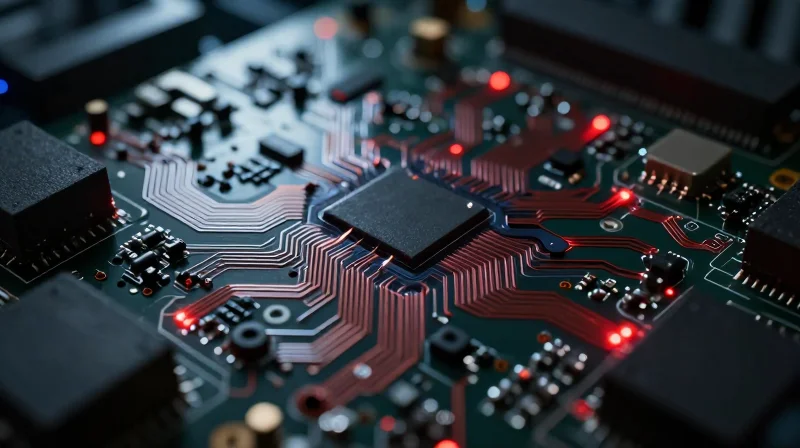
Iterative design flaws stemming from uncontrolled impedance represent a silent profit killer in high-speed electronics manufacturing. When signal integrity (SI) is compromised, designers are forced into repetitive board spins, each requiring new material procurement, assembly labor, and testing time. These unplanned costs extend far beyond the direct bill of materials, often cannibalizing R&D budgets intended for product innovation.
| Failure Stage | Economic Impact | ROI Impact |
|---|---|---|
| Prototyping | High labor costs/Materials | Delayed Validation |
| Pre-Production | Validation/Tooling Loss | Market Opportunity Loss |
| Market Release | Field Failure/Warranty | Brand Equity Erosion |
Quantifying the Cost of Ignorance
Failure to model stack-up requirements and trace geometries accurately forces engineers into a reactive stance. In high-speed domains, even a 5% deviation in impedance can lead to signal reflections and eye-diagram degradation that render a board assembly useless. The resulting diagnostic effort often outweighs the initial investment required to perform a comprehensive design-for-manufacturing (DFM) review.
- How does impedance control impact R&D cycle time?
Each iteration of a PCB board spin typically requires 2-4 weeks of fabrication and testing; multiple failures can push product launches months behind schedule, resulting in missed market windows. - What is the true cost of a failed prototype?
Beyond component costs, failures incur expensive engineering hours for root-cause analysis, laboratory overhead, and potential re-validation of regulatory compliance. - Why does SI failure often go undetected until final testing?
Without integrated impedance modeling, SI issues are often invisible to software-centric testing, only appearing when physical high-speed signal pathways encounter parasitic capacitance or inductance.
The Physics of Impedance in High-Speed Circuits

The Fundamentals of Impedance in GHz-Range Transmission
In high-speed digital systems, a PCB trace is not merely a copper path but a transmission line characterized by distributed resistance, inductance, capacitance, and conductance. When signals approach the gigahertz range, the wavelength becomes short enough that the electrical length of the trace matters significantly. If the impedance of the trace does not match the source and termination components, signal energy is reflected back toward the source, leading to ringing, overshoot, and significant jitter.
Managing Reflections and Signal Integrity
Reflections occur whenever a signal encounters a change in characteristic impedance. These reflections superimpose on the original signal, distorting the eye pattern and increasing the Bit Error Rate (BER). By maintaining a strictly controlled impedance profile, engineers ensure that electromagnetic energy travels efficiently along the interconnect, maximizing power transfer and preserving signal fidelity.
| Signal Phenomenon | Cause | Impact on ROI |
|---|---|---|
| Signal Reflection | Impedance Mismatch | Increased R&D and Re-spins |
| Crosstalk | Trace Proximity/Coupling | System Instability and Failure |
| Signal Attenuation | Dielectric Loss/Skin Effect | Reduced Transmission Distance |
- Why is 50-ohm impedance the industry standard?
50 ohms represents a calculated compromise between power handling capabilities and low signal attenuation for coaxial and PCB transmission lines. - How does manufacturing variation affect impedance?
Fluctuations in copper etching, dielectric constant (Dk), and layer thickness directly alter the geometry of the trace, causing impedance to deviate from the design target. - Does impedance control require additional cost?
While it adds a modest premium to PCB fabrication for testing and material verification, this investment yields a massive ROI by eliminating the need for expensive design iterations.
Case Study: Identifying the Bottleneck
Case Study: Identifying the Bottleneck
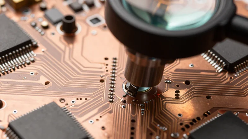
When a leading networking hardware firm faced a 15% failure rate in their latest 28 Gbps SerDes interface, the bottleneck was identified not at the component level, but within the physical PCB fabrication process. Intermittent data errors occurred primarily under thermal stress, pointing toward a systemic breakdown in signal integrity rather than isolated soldering defects.
Diagnostic Methodology
The diagnostic phase employed Time Domain Reflectometry (TDR) to map impedance profiles across the length of the differential pairs. By analyzing the reflected energy along the transmission lines, engineering teams were able to pinpoint localized impedance fluctuations that exceeded the ±5% target tolerance.
| Observed Metric | Expected Value | Actual Result | Impact |
|---|---|---|---|
| Differential Impedance | 100 Ω | 112 Ω | High Reflection |
| Trace Width | 4.5 mils | 3.8 mils | Inductance Spike |
| Bit Error Rate | <1e-12 | 1e-6 | Data Corruption |
Root Cause Analysis: Etch Factor Variation
The investigation determined that 'etch-back' during the copper removal process was non-uniform across the fabrication panel. Variations in the chemical bath chemistry resulted in trapezoidal trace profiles that deviated from the original design intent. These narrow traces significantly increased the characteristic impedance, resulting in signal reflections that triggered eye-diagram closure at high data rates.
- Why did thermal stress worsen the errors?
Thermal cycling expanded the dielectric substrate, exacerbating the already poor impedance matching at the junction of the narrowed traces and the pads, causing a complete loss of signal lock. - How was the process corrected?
We implemented a tighter etching duration protocol and adjusted the photolithography masks to compensate for expected chemical undercut, bringing the trace profiles back within the acceptable tolerance window.
Implementing Precision Impedance Control Protocols

Strategic Implementation of Impedance Protocols
To achieve reliable impedance control, manufacturers must move beyond reactive inspection to proactive design-stage validation. This involves the systematic integration of electromagnetic simulation, precise stack-up architecture, and rigorous material characterization to ensure that manufacturing variations stay within a tight tolerance of typically ±5%.
Optimizing Material and Stack-up Selection
Material selection serves as the foundation for impedance stability. Laminate Dk (Dielectric Constant) stability across temperature and frequency ranges is paramount. Engineers should prioritize materials with glass weave styles that mitigate 'fiber-weave effect' jitter, which can cause local impedance variations.
| Parameter | Standard FR-4 | High-Speed Laminate |
|---|---|---|
| Dk Stability | Low/Variable | High/Consistent |
| Loss Tangent | High (>0.02) | Low (<0.005) |
| Impedance Tolerance | ±10% | ±5% |
Frequently Asked Questions on Impedance Protocols
- How does stack-up optimization improve ROI?
By designing balanced symmetrical stack-ups, you reduce board warpage and eliminate the need for costly manufacturing re-spins, directly improving throughput. - Why is TDR testing considered the gold standard?
Time Domain Reflectometry (TDR) provides a spatial view of impedance discontinuities, allowing engineers to identify precisely which layer or trace segment is failing. - What role does copper surface roughness play?
Increased roughness increases insertion loss at higher frequencies, which can effectively shift your signal performance outside of the intended impedance window.
Improving Signal Integrity and System Throughput
The Direct Impact of Impedance Stability on Data Integrity
Signal integrity serves as the foundation for system throughput. When impedance remains consistent across every trace, signal reflections—often caused by discontinuities—are minimized. These reflections manifest as noise, rounding off the edges of digital pulses and closing the 'eye' in eye diagrams. By enforcing strict impedance tolerance, manufacturers can maintain open eye diagrams, enabling lower bit error rates (BER) and allowing designers to push clock speeds beyond original theoretical limits without compromising reliability.
| Parameter | Low Control Impact | High Control Impact |
|---|---|---|
| Eye Opening | Constricted/Closed | Wide/Clear |
| Bit Error Rate | Higher (High Noise) | Minimal (Low Noise) |
| System Throughput | Limited by Retries | Maximum Bandwidth |
Throughput Optimization and ROI
Precision impedance control acts as a catalyst for system ROI by reducing the need for costly troubleshooting, hardware revisions, and aggressive error-correction coding that consumes valuable processing overhead. When signal integrity is optimized at the board level, the hardware inherently supports higher data rates with fewer retransmissions, thereby increasing the effective bandwidth available to the end-user.
- How does impedance control reduce processing overhead?
Cleaner signals reduce the necessity for complex Forward Error Correction (FEC) algorithms, freeing up CPU or FPGA resources for primary tasks. - What is the relationship between impedance and jitter?
Impedance discontinuities cause reflections that introduce timing jitter; tighter control reduces this jitter, permitting tighter timing margins for faster signals. - Does impedance precision eliminate the need for signal conditioning?
While it significantly reduces signal degradation, it often allows for less expensive, low-power retimers rather than high-power signal conditioning components.
Impact on Total Cost of Ownership (TCO)

The Compounding Economics of PCB Iterations
The true cost of poor impedance control extends far beyond the price of the bare circuit board. When impedance tolerances drift, the resulting signal integrity issues often remain undetected until the late stages of the product development cycle—or worse, after deployment. By implementing rigorous precision impedance control protocols from the initial design phase, manufacturers move from a 'reactive correction' model to a 'right-first-time' manufacturing paradigm, drastically lowering the total cost of ownership.
| Cost Driver | Reactive Approach (Non-Controlled) | Proactive Approach (Precision Control) |
|---|---|---|
| Prototyping Cycles | 3-5 iterations due to signal noise | 1-2 iterations focused on optimization |
| Failure Analysis | High labor cost in field diagnostics | Minimal due to predictable performance |
| Time-to-Market | Delayed by re-spins | Accelerated by simulation accuracy |
| Yield Rates | Variable; high scrap rate | Stabilized; high throughput |
Financial Impact Analysis
When analyzing the TCO of high-speed boards, the hidden 'tax' on poorly controlled impedance includes the loss of board real estate, the necessity for over-engineering cooling or shielding to compensate for EMI, and the substantial cost of engineering man-hours dedicated to troubleshooting intermittent data errors. Investing upfront in precise material characterization and controlled dielectric thickness effectively pays for itself by reducing the cost of quality assurance and warranty-related service calls.
Frequently Asked Questions
- Why does initial precision increase manufacturing costs?
While precision materials and tighter manufacturing tolerances carry a higher per-unit cost, this is vastly offset by the elimination of multi-cycle design re-spins and the reduction of system-level failure rates. - How does impedance control affect long-term field costs?
Stable impedance reduces signal reflections and crosstalk, preventing degradation of signal integrity that often manifests as intermittent field failures, which are the most expensive type of failure to remediate.
Strategic Manufacturing Partnerships
Aligning Fabrication Capabilities with Signal Integrity Requirements
Selecting a PCB fabrication partner is not merely a logistical choice but a strategic technical decision that directly impacts the integrity of high-speed signals. When designing for precise impedance control, relying on standard fabrication tolerances often leads to latent defects that manifest only during final system integration. A partner with proven signal integrity expertise integrates design-for-manufacturing (DFM) feedback early, ensuring that material dielectric constants and etch factor compensations are tuned to meet tight impedance windows before the first board is ever etched.
The Risk of Commodity Fabrication vs. Specialized Partners
| Feature | Commodity Fabricator | Strategic SI Partner |
|---|---|---|
| Impedance Tolerance | Standard +/- 10% | Tight +/- 5% or better |
| Stack-up Modeling | Basic stack-up check | Full field-solver simulation |
| Design Engagement | Post-design DFM only | Collaborative pre-layout review |
| Failure Mitigation | Post-mortem reporting | Proactive simulation-based correction |
Key Questions for Evaluating Manufacturing Partners
- Do you perform internal field-solver impedance modeling?
A high-performance partner must demonstrate the use of advanced modeling tools to verify your stack-up against their specific manufacturing processes, rather than relying on generic calculator estimates. - How is material dielectric consistency tracked?
Ask for their process regarding Dk/Df validation; a partner should track batch-level material consistency to ensure that your impedance profile remains stable across high-volume production runs. - What is your approach to etch compensation for high-speed traces?
In high-speed designs, the shape of the trace cross-section affects impedance; ensure your partner understands how their specific chemical etching process alters trace geometries and accounts for this in their manufacturing compensation.
By moving beyond simple cost-per-board metrics to a model of technical partnership, organizations can effectively eliminate the 'impedance tax'—the hidden costs associated with board revisions, field failures, and debugging high-speed bus errors. A dedicated fabrication partner serves as an extension of your own engineering team, mitigating production risks through proactive communication and refined technical control.
By integrating rigorous impedance control at the earliest stages of design, companies can drastically reduce their risk profile and bottom-line costs. Don't let signal integrity issues compromise your next product launch. Contact our engineering team today to audit your PCB design process and ensure your high-speed projects cross the finish line on time and under budget.
