
In the race for market dominance, product miniaturization isn't just an aesthetic goal—it's a competitive necessity. As standard manufacturing hits a wall, Any-Layer HDI technology offers a clear path to high-performance scaling without the typical cost penalties.
The Evolution of HDI: From Stacking Vias to Any-Layer Freedom
The Sequential Build-up Era
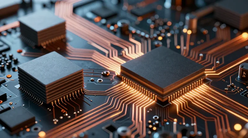
Early HDI technology relied heavily on Sequential Build-up (SBU) processes. Designers were restricted to specific layer-to-layer connections, often forced into staggered via configurations to maintain structural integrity and manufacturing yields. This constraint limited signal routing density and forced engineers to sacrifice board real estate to accommodate complex via transitions.
The Transition to Stacking and Beyond
As device footprints shrunk, the industry moved toward 'stacked' via structures. By stacking microvias directly on top of one another, designers achieved higher density, but this introduced significant thermal and mechanical reliability risks. Any-Layer HDI (AL-HDI) emerged as the definitive solution, removing the 'via-in-pad' and sequential stacking constraints by allowing microvias to exist between any two layers.
| Technology Feature | Sequential HDI | Any-Layer HDI |
|---|---|---|
| Via Placement | Layer-to-layer restricted | Full flexibility (Any-to-Any) |
| Routing Density | Moderate | Extreme |
| Board Footprint | Larger | Optimized/Minimal |
| Design Complexity | Manageable | High (requires advanced EDA) |
Key Advantages for Market Acceleration
- How does AL-HDI reduce time-to-market?
By eliminating the need for rigid sequential stacking constraints, engineers can finalize board layouts faster, reducing the number of design iterations required to resolve complex routing congestion. - Why is Any-Layer architecture more reliable?
AL-HDI distributes structural stress more evenly across the board compared to traditional stacked via designs, which often suffer from localized stress concentration points. - Does this technology impact signal integrity?
Yes; the ability to route signals vertically across any layer pair significantly shortens signal paths, drastically reducing parasitic capacitance and latency in high-speed, ultra-miniature designs.
Why Traditional HDI Fails to Meet Modern Miniaturization Demands
The Architectural Bottlenecks of Traditional HDI
Traditional HDI, characterized by sequential lamination and fixed via-staggering, is increasingly inadequate for devices requiring high-density interconnects in compact footprints. The primary failure point lies in the physical constraints imposed by rigid build-up layers, which limit routing flexibility and force designers to compromise on board area and signal integrity. As pin counts for high-speed processors and connectivity chips increase, standard via structures become the primary limiting factor for miniaturization.
Comparative Analysis: Traditional vs. Any-Layer HDI
| Feature | Traditional HDI | Any-Layer HDI |
|---|---|---|
| Via Placement | Restricted to specific layers | Any layer to any layer |
| Routing Density | Limited by via stacking rules | Maximum density/unrestricted |
| Signal Performance | Higher parasitic interference | Lower latency/improved integrity |
| Design Cycle | Iterative and time-consuming | Streamlined/Faster time-to-market |
Common Challenges in Traditional Designs
- Why does sequential lamination slow down development?
Each lamination cycle adds significant time to the manufacturing process and forces rigid design rules that limit where vias can be placed, often requiring multiple redesigns to route high-pin-count components. - How does routing inefficiency impact ROI?
Inefficient routing leads to larger board sizes and increased layer counts, driving up material costs and production complexity, which directly erodes the projected return on investment for high-end consumer devices. - What role does signal integrity play in HDI failure?
Traditional via structures often necessitate longer trace lengths and non-optimal signal paths, which can introduce crosstalk and impedance discontinuities in high-speed, miniaturized circuits.
Economic Advantages: Calculating the True Cost of Any-Layer HDI

The Economic Trade-off: Beyond Unit Cost
While Any-Layer HDI carries a higher initial board-level fabrication price, the true economic advantage emerges in system-level cost savings and time-to-market acceleration. By enabling extreme miniaturization, designers can condense multiple PCBs into a single layer-dense board, reducing housing dimensions, connector requirements, and total assembly weight. This holistic reduction offsets the premium on fabrication, leading to a leaner bill of materials (BOM).
| Metric | Traditional Sequential HDI | Any-Layer HDI |
|---|---|---|
| Board Size | Large (due to fan-out constraints) | Small (optimized density) |
| Assembly Complexity | High (multiple boards/cables) | Low (single unified PCB) |
| Unit Fabrication Cost | Lower | Higher |
| System ROI | Moderate | High (optimized footprint) |
Strategic Financial Justifications
- Why does Any-Layer HDI accelerate time-to-market?
The ability to route anywhere in the board eliminates complex trace serpentine paths and reduces layout cycle times, allowing engineers to bypass design-cycle bottlenecks. - How does this technology improve yield?
Any-Layer construction reduces the reliance on stacked microvias that are prone to mechanical stress failure, leading to higher long-term reliability and fewer warranty claims. - What is the impact on secondary assembly costs?
By simplifying the interconnect architecture, you significantly reduce the labor and components required for inter-board communication and structural mounting.
Ultimately, the decision to invest in Any-Layer HDI must be evaluated against the Total Cost of Ownership (TCO). Companies that prioritize board unit pricing over total system footprint often incur hidden costs through slower assembly and larger device enclosures. For ultra-miniature hardware, Any-Layer HDI serves not merely as a component, but as an enabling technology for market leadership.
Optimizing PCB Real Estate and Signal Integrity
Unlocking Routing Density Through Any-Layer Interconnects
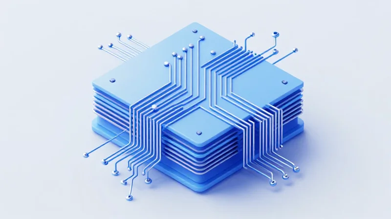
Any-Layer HDI eliminates the constraints of traditional via-in-pad or staggered via structures by allowing any layer to be connected to any other layer with microvias. This freedom maximizes routing density, allowing engineers to shrink footprints while maintaining high electrical performance. By reducing the reliance on multiple through-hole vias, designers can reclaim significant surface area and internal volume, allowing for denser component placement without compromising signal paths.
Impact on Signal Integrity
Shorter interconnects are the cornerstone of superior signal integrity in high-frequency designs. Any-Layer HDI reduces parasitic inductance and capacitance by minimizing via stubs and shortening signal trace lengths. This reduction is critical for high-speed differential pairs where signal reflections and electromagnetic interference must be strictly controlled to maintain signal fidelity.
| Feature | Traditional HDI | Any-Layer HDI |
|---|---|---|
| Routing Flexibility | Layer-to-layer restricted | Total layer freedom |
| Via Structure | Staggered/Stacked limit | All-layer microvias |
| Signal Path Length | Moderate/Long | Minimal |
| Board Footprint | Larger | Compact |
Design Efficiency FAQ
- How does Any-Layer HDI reduce layer counts?
By allowing efficient vertical routing between adjacent and non-adjacent layers, engineers can pack more signals into fewer total board layers, effectively reducing the overall thickness and cost of the laminate stack-up. - Does this technology improve EMC performance?
Yes, by providing shorter signal paths and better return path management through localized microvias, Any-Layer HDI significantly reduces loop areas that typically contribute to electromagnetic interference.
Case Study: Achieving 30% Footprint Reduction in Wearable Tech

The Challenge: Breaking Physical Barriers in Wearable Design
A tier-one wearable manufacturer faced a critical development bottleneck: the integration of advanced sensors and high-capacity batteries necessitated a smaller PCB footprint, yet standard HDI via-in-pad technologies were exhausted. The design team struggled with routing congestion that threatened to delay the product launch by six months, creating a direct conflict between feature density and time-to-market goals.
Strategic Implementation of Any-Layer HDI
By migrating to Any-Layer HDI, the engineering team eliminated the need for through-hole vias, allowing for arbitrary point-to-point interconnects between any layers. This shift fundamentally changed the design paradigm, enabling the team to reclaim 30% of the board area previously lost to routing keep-outs and thermal relief patterns.
| Metric | Standard HDI | Any-Layer HDI | Improvement |
|---|---|---|---|
| Board Footprint | 1200 mm² | 840 mm² | 30% Reduction |
| Routing Layers | 12 Layers | 8 Layers | 33% Complexity Drop |
| Signal Integrity Margin | Baseline | High | Improved EMI |
Key Lessons from the Field
- How did Any-Layer HDI shorten the schedule?
The increased routing flexibility reduced the number of design iterations required to resolve congestion, cutting the pre-production validation phase by 40%. - Was there a trade-off in manufacturing costs?
While unit costs for Any-Layer boards were higher, the total cost of ownership dropped due to the reduced board size and fewer layers, which lowered material consumption and assembly time. - What was the impact on signal integrity?
Shorter trace paths and reduced via stub counts minimized parasitic inductance, resulting in a more robust RF performance without additional shielding components.
Streamlining Complex Assembly Processes
Simplifying Via-in-Pad Architectures
Traditional HDI designs often rely on complex dog-bone fan-out structures that create assembly bottlenecks. By transitioning to Any-Layer HDI with true via-in-pad capability, engineers can place interconnects directly within the component pads. This eliminates the need for lateral fan-out routing, drastically reducing the surface area required for mounting and minimizing the risk of solder bridging or misalignment during high-speed reflow processes.
Comparative Efficiency: Traditional HDI vs. Any-Layer HDI
| Assembly Parameter | Traditional HDI | Any-Layer HDI |
|---|---|---|
| Routing Strategy | Dog-bone fan-out | Direct via-in-pad |
| Placement Tolerance | Higher risk/Complex | Lower risk/Streamlined |
| Solder Paste Control | Difficult | Excellent |
| Assembly Speed | Standard | Optimized |
Strategic Advantages in Assembly Precision
Beyond the technical routing benefits, Any-Layer HDI facilitates a more robust SMT (Surface Mount Technology) assembly environment. Because pads are perfectly planar and integrated with vertical interconnects, the stability of fine-pitch components like 0201 or 01005 passives is significantly improved during the pick-and-place operation.
- How does via-in-pad technology reduce error rates?
By allowing direct vertical connections, it eliminates complex lateral traces that act as potential points of failure or pathways for solder wicking, leading to cleaner, more reliable joints. - Does Any-Layer HDI affect production throughput?
Yes, it enables higher component density per square millimeter and requires fewer board layers, which results in shorter thermal cycles and faster throughput on the assembly line. - Why is planar surface integrity critical?
A planar landing surface ensures consistent solder paste deposition, which is essential for achieving high yields in miniaturized, high-density electronic assemblies.
Accelerating Time-to-Market: The Design-to-Prototype Pipeline

Accelerating the Design-to-Prototype Pipeline
The transition from concept to functional prototype is often hampered by rigid design rules that mandate multiple revisions. Any-Layer HDI technology eliminates these bottlenecks by providing 'any-layer-to-any-layer' connectivity, which removes the traditional constraints of stack-up limitations and staggered via structures. By utilizing copper-filled microvias in any layer, designers gain unprecedented routing freedom, allowing them to iterate faster and reduce the number of respins required to meet signal integrity targets.
Efficiency Gains: Traditional HDI vs. Any-Layer HDI
| Feature | Traditional HDI | Any-Layer HDI |
|---|---|---|
| Via Structure | Staggered/Sequential | Copper-filled Stacked |
| Design Iterations | High (Constraint-heavy) | Low (High-routing freedom) |
| Time-to-Market | Baseline | 30-40% Faster |
Strategies for Rapid Integration
To maximize the ROI of Any-Layer HDI, firms must adopt a concurrent engineering approach. Early collaboration with PCB fabricators ensures that the stack-up is optimized for manufacturability (DFM) from day one, preventing late-stage design changes. Leveraging advanced CAD simulation tools to account for the increased density early in the layout process allows for precise thermal and signal integrity validation before the first board is even printed.
Frequently Asked Questions
- Why does Any-Layer HDI reduce total design time?
It allows for tighter component placement and complex routing that would otherwise require multiple extra layers or increased board surface area, bypassing the need for extensive redesigns. - How does this impact the prototyping phase?
The ability to route complex BGA patterns in a smaller footprint minimizes signal traces and crosstalk, increasing the likelihood that the first prototype will pass signal integrity testing on the first run. - What is the primary risk to avoid when scaling?
Avoid ignoring DFM guidelines early in the cycle, as Any-Layer HDI requires precise material matching and thermal management strategies to ensure long-term reliability.
Selecting the Right Manufacturing Partner for HDI Success
Core Competencies for Any-Layer HDI Partners
The transition to any-layer HDI technology represents a significant leap in PCB complexity, requiring a partner that offers more than basic fabrication services. To guarantee project success and maximize ROI, you must evaluate a fabricator’s mastery of laser via formation, precision lamination, and registration tolerances. Partners lacking rigorous process controls in these areas often face low yields, which directly offsets the time-to-market advantages that HDI technology is intended to provide.
- What is the primary indicator of a capable HDI partner?
Look for proven consistency in 'via-in-pad' copper plating and laser drilling depth control. A top-tier partner will share yield statistics specifically related to their fine-pitch interconnect processes. - How does material selection impact manufacturing reliability?
Any-layer HDI requires advanced thin laminates with specific coefficients of thermal expansion (CTE). An ideal partner will offer DFM (Design for Manufacturing) feedback regarding material stack-ups to prevent warping and ensure signal integrity.
Evaluation Matrix: Tier-1 vs. Standard Fabricators
| Capability Category | Standard PCB Fabricator | HDI Specialized Partner |
|---|---|---|
| Laser Via Precision | Limited depth/accuracy | Nanosecond/Picosecond laser control |
| Registration Tolerance | Standard +/- 2-3 mils | Advanced +/- 0.5-1 mil |
| Stack-up Design | Reactive approach | Proactive DFM/Signal integrity analysis |
| Quality Certification | ISO 9001 only | AS9100/Medical Grade (ISO 13485) |
Strategic Vetting Questions
Before finalizing your partnership, audit your potential vendor using these strategic benchmarks: Can they demonstrate automated optical inspection (AOI) capabilities that detect sub-micron defects? Do they maintain an in-house lab for micro-sectioning and cross-sectional analysis? Most importantly, request a 'DFM review' on your initial files; a partner that proactively suggests design optimizations to improve manufacturing yield is your most valuable asset in accelerating your product's release cycle.
By embracing Any-Layer HDI, companies can solve complex spatial constraints while simultaneously driving down assembly overhead and maximizing board performance. If you are ready to shrink your footprint and improve your ROI, contact our engineering team today for a consultation on your next high-density design project.
