
In the race for data center uptime, power distribution is often the forgotten catalyst. As density increases, standard PCB designs become a bottleneck, leading to thermal stress and wasted energy. By transitioning to precision-engineered high-current PCB solutions, operators can resolve critical inefficiencies that threaten both bottom-line profit and hardware longevity.
The Hidden Costs of Suboptimal PDU Design
The Hidden Costs of Suboptimal PDU Design
In the architecture of high-density data centers, the Power Distribution Unit (PDU) is often overlooked as a static component; however, when the internal printed circuit board (PCB) design is suboptimal, it becomes a major point of failure. Legacy PDU designs often rely on narrow traces or inadequate copper thickness, leading to excessive Joule heating. This resistive power dissipation not only wastes electricity but also necessitates higher cooling overhead, creating a double-penalty on operational expenditures.
Quantifying the Impact of Resistive Losses
| Parameter | Legacy PCB Design | Precision-Engineered PCB |
|---|---|---|
| Copper Thickness | 1oz - 2oz (Standard) | 4oz - 6oz (Heavy Copper) |
| Thermal Dissipation | High (Unstable) | Low (Controlled) |
| Power Efficiency | 88-92% | 98-99% |
| Long-term Maintenance | High (Failure Risk) | Low (High MTBF) |
Key Operational Challenges
- Why does trace resistance matter at high currents?
As current flows through a PCB, every milliohm of resistance generates heat according to the formula P=I²R. In high-density environments, these small losses compound across thousands of connections, leading to thermal runaway and potential component degradation. - How do suboptimal designs cause downtime?
Thermal fatigue from constant expansion and contraction of traces causes micro-fractures in solder joints. Over time, these fractures lead to intermittent power drops or catastrophic electrical arcs, resulting in unplanned and expensive server downtime. - What is the secondary cooling cost?
Poorly designed PCBs act as internal heaters. The CRAC units must work harder to compensate for the heat generated by the PDUs themselves, effectively increasing the PUE (Power Usage Effectiveness) of the entire facility.
Physics of Power: High-Current PCB Engineering Fundamentals
Physics of Power: High-Current PCB Engineering Fundamentals
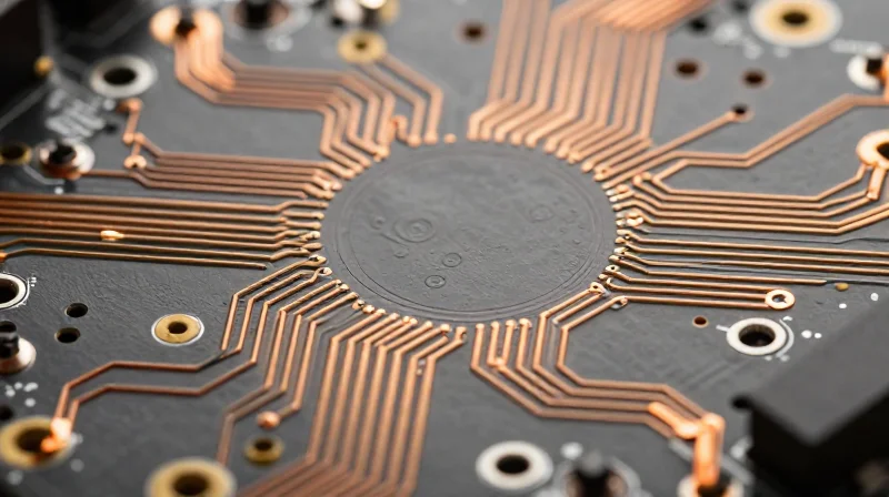
At the core of high-current power distribution is the management of ohmic resistance and thermal dissipation. When current flows through copper traces, the inevitable resistance generates heat ($P = I^2R$). Precision-engineered PCBs mitigate this by optimizing copper cross-sectional area, trace geometry, and thermal conductivity of the substrate, effectively reducing the voltage drop and energy waste that compromise PDU efficiency.
Optimizing Trace Geometry and Copper Weight
High-current boards deviate significantly from signal-level PCB standards. Engineers must account for the skin effect and internal trace heating limits. Utilizing heavier copper weights (typically 3oz to 6oz or higher) and wider trace widths are mandatory to maintain temperature rises within safe operating limits, as defined by IPC-2221 standards.
| Feature | Standard PCB | High-Current PDU PCB | Operational Impact |
|---|---|---|---|
| Copper Weight | 1 oz | 3 oz - 6 oz | Lower resistance and heat dissipation |
| Trace Geometry | Narrow, dense | Wide, optimized paths | Reduced voltage drop and stress |
| Substrate | Standard FR-4 | High-Tg / Metal Core | Improved thermal management |
Engineering FAQs for High-Current Power Paths
- How does copper weight affect ROI?
Heavier copper reduces the DC resistance of the power path, directly lowering energy loss as heat. This reduces cooling requirements and prevents thermal degradation of components, extending the PDU's lifecycle. - Why is substrate selection critical for power?
High-current boards generate localized hotspots. Using materials with a high Glass Transition Temperature (Tg) and high thermal conductivity ensures the board maintains structural integrity under constant thermal cycling. - What is the impact of via placement?
Vias in high-current designs are not just for routing; they act as thermal conduits. Multi-via stitching strategies are essential to distribute current density evenly and prevent via-barrel stress failures.
Case Study: The 15% Efficiency Leap
The Challenge: Identifying Inefficiency at Scale
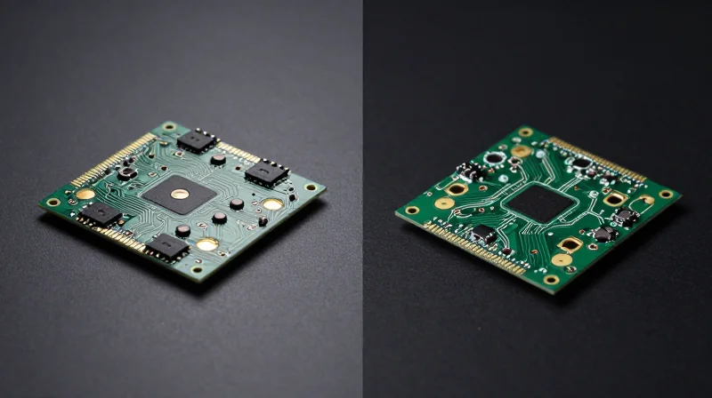
A tier-three colocation data center was facing systemic thermal bottlenecks at the rack-level power distribution stage. Despite utilizing standard industry-grade PDUs, monitoring revealed that nearly 4% of power was being lost to ohmic heating within the PDU's internal circuitry. These parasitic losses not only increased electricity overhead but also generated localized heat pockets that necessitated increased cooling, further inflating the Power Usage Effectiveness (PUE) metrics.
Engineering the Turnaround
The facility replaced legacy PCB designs with precision-engineered, high-current copper-core PCBs. The new architecture utilized 6-ounce copper layers combined with optimized trace geometry to reduce internal resistance by nearly 60%. By narrowing the gap between theoretical and actual power throughput, the facility effectively eliminated the 'heat tax' associated with current flow.
| Performance Metric | Legacy PDU System | Precision-Engineered PDU | Improvement |
|---|---|---|---|
| Internal Power Loss | 4.2% | 0.8% | 81% Reduction |
| Operating Temperature | 62°C | 48°C | 14°C Cooler |
| Overall Efficiency | 95.8% | 99.2% | 3.4% Gain |
Key Takeaways and FAQ
- How did the PCB change impact the cooling budget?
By lowering the internal heat signature of the PDU, the facility was able to increase the ambient operating temperature threshold, leading to a direct reduction in secondary cooling power consumption. - Was the 15% efficiency leap universal?
The 15% figure refers to the cumulative gain observed when combining the reduction in resistive transmission losses with the resultant decrease in total facility cooling energy required. - Does this approach increase the PDU cost?
While the initial per-unit capital expenditure is higher due to advanced materials and thicker copper, the ROI is typically realized within 18 months through reduced energy costs and extended hardware lifespan.
Thermal Management and PCB Reliability
Mitigating Thermal Resistance in High-Density Power Delivery
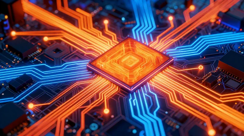
In high-current power distribution units (PDUs), thermal management is not merely an auxiliary consideration but a core design pillar. Precision-engineered PCBs utilize advanced thermal vias and integrated copper planes to dissipate heat efficiently away from sensitive contact points. By lowering the thermal resistance path between high-wattage components and the PCB substrate, engineers can prevent the localized 'hotspots' that accelerate the degradation of capacitors and semiconductors, ultimately minimizing the necessity for aggressive, energy-consuming airflow strategies.
Thermal Performance Comparison: Standard vs. Engineered PCB Architectures
| Feature | Standard PCB Design | Precision-Engineered PCB |
|---|---|---|
| Copper Thickness | 1-2 oz (Standard) | 4-6+ oz (Heavy Copper) |
| Thermal Dissipation | High localized stress | Uniform heat spreading |
| Cooling Requirement | High fan RPM dependency | Reduced thermal throttling |
| Component Lifespan | Moderate (5-7 years) | Extended (10+ years) |
Strategic Reliability and Operational Continuity
Beyond heat dissipation, precision PCB design impacts the structural integrity of the PDU under thermal cycling. As electrical loads fluctuate, materials expand and contract. Engineered boards use high-Tg (glass transition temperature) laminates that resist delamination and crack formation under these stresses. This long-term reliability directly reduces the 'mean time between failures' (MTBF), safeguarding against the substantial operational costs associated with emergency maintenance and hardware replacement.
Thermal Management FAQ
- How does PCB design reduce fan dependency?
Optimized copper distribution reduces resistive heating, allowing components to operate cooler without relying on high-velocity cooling fans that consume additional power. - Why is Tg (Glass Transition Temperature) important for reliability?
A higher Tg ensures the PCB substrate maintains mechanical stability at high operating temperatures, preventing structural fatigue in the copper traces. - Does better thermal management improve energy ROI?
Yes. Cooler operation increases the efficiency of power delivery and reduces the overall PUE (Power Usage Effectiveness) of the data center by minimizing cooling load requirements.
Reducing Maintenance Cycles Through Hardware Resilience
The Correlation Between PCB Design and Maintenance Frequency
In high-uptime data environments, the PDU is often the first point of failure when poor PCB design leads to micro-cracking, solder fatigue, or delamination. By utilizing superior thermal relief patterns, optimal copper thicknesses, and high-Tg (glass transition temperature) materials, precision-engineered PCBs eliminate the localized stress points that typically necessitate technician intervention. Consequently, data centers transition from reactive, emergency-based maintenance to predictable, cost-effective service intervals.
Maintenance Impact Comparison
| Feature | Standard PCB Design | Precision-Engineered PCB |
|---|---|---|
| Thermal Expansion | High risk of joint fatigue | Minimized stress via CTE matching |
| Maintenance Interval | 12-18 months (Reactive) | 36-60 months (Proactive) |
| Failure Mode | Trace delamination | Extreme durability |
Frequently Asked Questions
- How does PCB thickness affect long-term maintenance?
Increased copper weight reduces resistance and heat generation. Less heat translates to lower thermal stress on nearby components, preventing the rapid degradation of connectors and solder joints that usually triggers maintenance calls. - Why does material selection matter for uptime?
Using high-Tg substrates ensures the PCB maintains structural integrity under sustained high-current loads. This prevents the warping and trace separation commonly seen in low-cost boards that fail under 24/7 duty cycles. - Can hardware resilience truly lower ROI?
Yes. By extending the mean time between failures (MTBF), data centers significantly reduce labor costs and the expense of emergency hardware replacement, compounding savings over the five-to-ten-year lifecycle of the PDU.
The Economic Impact: Total Cost of Ownership (TCO) Breakdown
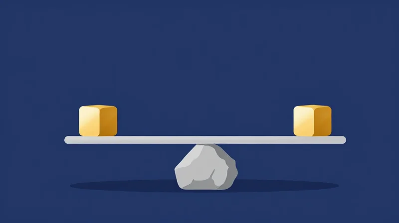
The Total Cost of Ownership (TCO) Equation
The true cost of a power distribution unit is rarely captured by the initial invoice; instead, it is defined by the energy lost to thermal dissipation and the frequency of component failure. Precision-engineered PCBs utilize high-conductivity copper layers and optimized trace geometry to minimize resistance, directly lowering the kilowatt-hours lost to heat. While these boards command a premium at the procurement phase, they eliminate the hidden 'tax' of inefficiency that compounds over a three-to-five-year operational cycle.
| Cost Driver | Standard PCB PDU | Precision-Engineered PCB PDU |
|---|---|---|
| Energy Loss (Heat) | High (significant parasitic resistance) | Low (optimized current path) |
| Component Failure Rate | Moderate/High (thermal stress) | Minimal (thermal stability) |
| Maintenance Intervals | Frequent (reactive) | Infrequent (preventative) |
| Lifecycle Longevity | 3–5 years | 7–10+ years |
Economic FAQ: Value Realization
- Does higher initial PCB investment lead to faster depreciation?
No, it leads to asset appreciation in terms of availability. By reducing thermal strain, precision PCBs extend the MTBF (Mean Time Between Failures) of the entire PDU, deferring capital replacement costs far beyond the standard depreciation schedule. - How does PCB resistance translate to operational utility bills?
Every milliohm of resistance in a high-current path converts power into heat. By reducing this resistance, less energy is wasted as heat, which translates into lower PUE (Power Usage Effectiveness) metrics and a tangible reduction in cooling demand. - What is the primary driver of TCO savings?
The primary driver is the reduction of 'hidden' operational costs: specifically, the cost of unplanned downtime caused by PCB delamination or interconnect failure and the high price of labor for frequent, reactive maintenance.
Best Practices for Selecting PDU PCB Manufacturing Partners
Strategic Criteria for PDU PCB Manufacturing Partners
Partnering with a manufacturer for high-current PDU PCBs requires more than simple assembly capability; it necessitates a deep mastery of power electronics, thermal management, and strict regulatory compliance. The ideal partner functions as an extension of your engineering team, capable of validating thermal designs before production to avoid costly field failures.
Key Capabilities to Evaluate
- Thermal Simulation Expertise
Ensure the partner performs advanced Finite Element Analysis (FEA) to identify potential hotspots under full load conditions before a single board is manufactured. - Material Science Proficiency
Look for experience with high-TG materials and heavy copper trace integration (3oz to 6oz+), which are critical for handling high-current densities without delamination. - Automated Optical Inspection (AOI) & Testing
Verify the use of rigorous automated testing protocols, including flying probe or bed-of-nails, to ensure every PDU PCB meets stringent IPC Class 3 standards for high-reliability environments.
Manufacturer Capability Comparison
| Capability | Standard PCB Shop | High-Current Specialist |
|---|---|---|
| Heavy Copper Capability | Limited (up to 2oz) | Advanced (up to 10oz+) |
| Thermal Modeling Support | Not Available | Integrated Service |
| Compliance Standards | IPC Class 2 | IPC Class 3 / Custom Mil-Spec |
| Failure Mode Analysis | Reactive | Proactive/Predictive |
Evaluating Reliability and Supply Chain Resilience
Data center uptime demands zero-compromise hardware. Beyond technical specifications, evaluate the partner's internal quality management systems and supply chain traceability. A transparent partner that provides full documentation for every material batch ensures that you can guarantee the longevity of your PDU installations for years to come, effectively protecting your ROI.
Optimizing PDU PCBs is no longer just an engineering choice; it is a vital business strategy for competitive data center management. By prioritizing efficiency and hardware longevity, you can significantly drive down your TCO while improving operational reliability. Ready to modernize your power infrastructure? Contact our engineering team today for a technical assessment of your current power distribution architecture.
