
In the race to launch expansive satellite constellations, the upfront pressure to reduce manufacturing costs often creates a hidden, long-term fiscal liability. For LEO and GEO missions, the true cost of a PCB isn't found in the initial purchase order, but in the mission-ending failures caused by signal degradation and premature hardware decay. This analysis examines why precision-engineered, high-reliability PCB fabrication is the most effective investment for ensuring long-term mission success and financial efficiency.
The Economics of Reliability in Orbit
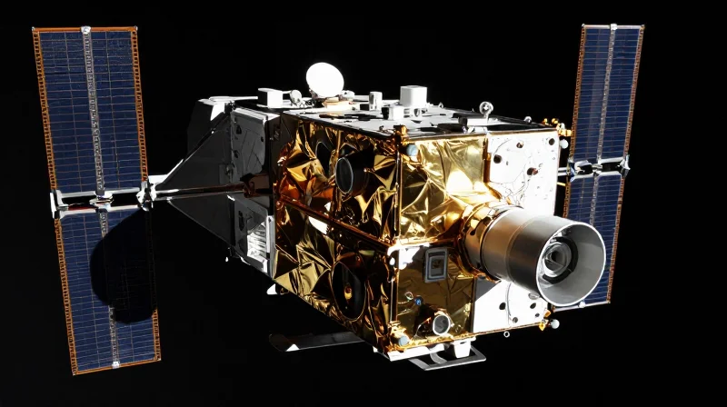
The Asymmetric Cost of Hardware Failure
In the orbital environment, the economics of hardware failure are fundamentally asymmetric. The financial investment required to design, manufacture, and launch a satellite is a sunk cost that dwarfs the incremental premium paid for superior high-frequency PCB materials and rigorous manufacturing tolerances. When a mission fails due to component degradation or signal integrity loss, the loss is not merely the cost of the PCB, but the total loss of the launch vehicle capacity, insurance premiums, and years of operational potential.
| Economic Factor | Low-Cost Component Strategy | Precision Manufacturing Strategy |
|---|---|---|
| Unit Manufacturing Cost | Low | Higher |
| Probability of Mission Loss | Increased | Minimized |
| Total Mission ROI | High Risk of Total Failure | Optimized Lifecycle Value |
| Risk Mitigation Expense | Reactive (Insurance/Claims) | Proactive (Quality Assurance) |
Critical Economics of Material Selection
High-frequency signal stability is highly dependent on dielectric consistency under extreme thermal cycling. Inferior PCB laminates often suffer from coefficient of thermal expansion (CTE) mismatches, leading to micro-cracks and interconnect failures that are impossible to repair once the craft has reached orbit. By selecting high-performance substrates that maintain structural integrity across wide temperature swings, manufacturers effectively purchase an insurance policy against the most common modes of orbital electronic failure.
Frequently Asked Questions
- Does precision manufacturing increase launch costs?
No. By increasing reliability, precision manufacturing reduces the need for heavy redundancy, ultimately allowing for leaner, more optimized mission designs that can potentially fit into lower-cost launch profiles. - Is the material cost premium justifiable for smallsats?
Yes. Even for smallsat constellations, the loss of a single node in a network can disrupt the entire mission service level agreement (SLA), making the material premium a negligible fraction of the total operational value. - How does PCB manufacturing impact long-term mission ROI?
Precision-manufactured PCBs extend the operational lifespan of the satellite by ensuring component stability, enabling the mission to stay profitable well beyond its initial breakeven point.
Signal Integrity as a Performance Asset

The Direct Correlation Between Signal Integrity and Throughput
In modern satellite constellations, the high-frequency front-end acts as the bottleneck for spectral efficiency. When signal integrity is compromised due to manufacturing variances or sub-optimal material selection, the resultant jitter and insertion loss necessitate more robust error correction overhead, effectively cannibalizing the usable data rate. Maximizing ROI begins by treating signal integrity not as a design constraint, but as a performance asset that permits higher-order modulation schemes and increased channel density.
Material Impact on Propagation Performance
| Parameter | Standard FR-4 Impact | High-Frequency Laminate Benefit |
|---|---|---|
| Dielectric Constant (Dk) Stability | High variance across frequency | Stable for predictable impedance |
| Dissipation Factor (Df) | High loss (signal attenuation) | Ultra-low loss (signal retention) |
| Thermal Expansion (CTE) | Mismatched, causing via fatigue | Balanced for orbital cycling |
Key Considerations for Mission Success
- How does copper roughness affect high-frequency signals?
At millimeter-wave frequencies, the skin effect confines current flow to the surface of the copper traces. Rough surface profiles increase path length and resistance, leading to insertion loss and phase distortion that degrade constellation bandwidth. - Why is impedance control critical for satellite constellations?
Impedance discontinuities cause signal reflections that manifest as bit errors. In a space environment, minimizing these reflections through precise manufacturing ensures the lowest possible bit error rate (BER), reducing the need for power-intensive retransmissions. - Does material optimization provide a long-term financial edge?
Yes, by utilizing materials with low moisture absorption and stable dielectric constants, satellites maintain consistent performance over years of thermal cycling, significantly extending the operational life and revenue-generating capacity of the asset.
Material Science: The First Line of Defense
Material Science: The First Line of Defense
In the vacuum of space, Printed Circuit Board (PCB) reliability is fundamentally tied to the molecular stability of substrate materials. Unlike terrestrial electronics, satellite hardware faces extreme thermal cycling—fluctuating rapidly between extreme cold in shadow and intense solar heating. To maximize mission ROI, engineers must prioritize high-glass transition temperature (Tg) laminates and specialized low-loss dielectrics to prevent structural delamination and signal degradation over multi-year lifecycles.
Mitigating Thermal Fatigue
The Coefficient of Thermal Expansion (CTE) is the most critical material property in orbit. When the CTE of the copper traces significantly differs from that of the dielectric substrate, thermal cycling leads to barrel cracking in vias and interfacial separation. By utilizing materials with a low, uniform CTE—specifically in the Z-axis—manufacturers can prevent mechanical fatigue that leads to catastrophic signal failure.
| Material Property | Standard FR-4 | Space-Grade Laminate | Impact on ROI |
|---|---|---|---|
| Glass Transition (Tg) | 130-140°C | >200°C | Prevents warping during thermal cycling |
| Loss Tangent | 0.020 | <0.003 | Reduces signal attenuation at high frequency |
| Z-Axis CTE | High (>70 ppm/°C) | Low (<30 ppm/°C) | Ensures via integrity and reliability |
Key Considerations for Dielectric Selection
- Why is the Dissipation Factor (Df) vital for space applications?
A lower Df minimizes energy loss as heat within the dielectric. In constrained satellite power budgets, preserving signal strength prevents the need for additional amplification, thereby reducing thermal load and power consumption. - How does moisture absorption affect orbital performance?
Even trace amounts of absorbed moisture can outgas in a vacuum, potentially contaminating sensitive optical sensors. Using low-hygroscopic materials is essential for maintaining both structural integrity and mission-critical hardware cleanliness. - Is Tg the only factor for thermal survival?
No; while a high Tg prevents the substrate from transitioning to a rubbery state, the thermal conductivity of the material is also vital for heat dissipation away from high-density processing components.
Reducing Rework Cycles and Schedule Risk

The Cost of Design Iterations in Space Programs
In the context of satellite constellations, a single design revision late in the development cycle is rarely just a software update; it triggers a cascade of mechanical, thermal, and regulatory re-validations. Rework cycles often stem from discrepancies between initial board layout simulations and the physical realities of high-frequency manufacturing. By adopting a 'zero-defect' approach to PCB design, mission leads can avoid the prohibitive costs associated with assembly delays, re-testing phases, and the potential for a launch window to be missed entirely.
Strategic DFM Implementation
| Risk Factor | Manufacturing Impact | Mitigation Strategy |
|---|---|---|
| Signal Skew | Data loss/Bit errors | Controlled impedance and matched trace length verification |
| Thermal Mismatch | Solder joint fatigue | CTE-matched laminate selection |
| Plating Voids | Interconnect failure | Advanced drill cycle optimization and micro-via inspection |
Reducing Schedule Risk via Precision Fabrication
Schedule risks are frequently minimized when manufacturers move beyond standard PCB production into precision high-frequency fabrication. Using integrated simulation tools during the pre-production phase allows for the identification of potential manufacturing bottlenecks—such as plating thickness variations or dielectric loss anomalies—before the physical board is fabricated. Proactive collaboration ensures that manufacturing constraints are accounted for in the CAD environment, creating a predictable, repeatable process that aligns with strict satellite launch cadences.
- How does early DFM engagement reduce rework?
Early engagement identifies complex routing or stack-up issues that lead to production failures, allowing for adjustments while the design is still virtual. - What role does automation play in schedule risk?
Automated Optical Inspection (AOI) and laser-directed registration processes reduce human error and turnaround time, ensuring high-frequency boards meet specs on the first build. - Is testing part of the rework mitigation cycle?
Yes, rigorous pre-fabrication modeling combined with automated test protocols minimizes the need for iterative prototyping and post-fabrication troubleshooting.
Case Study: Comparing Standard vs. High-Reliability Fabrication
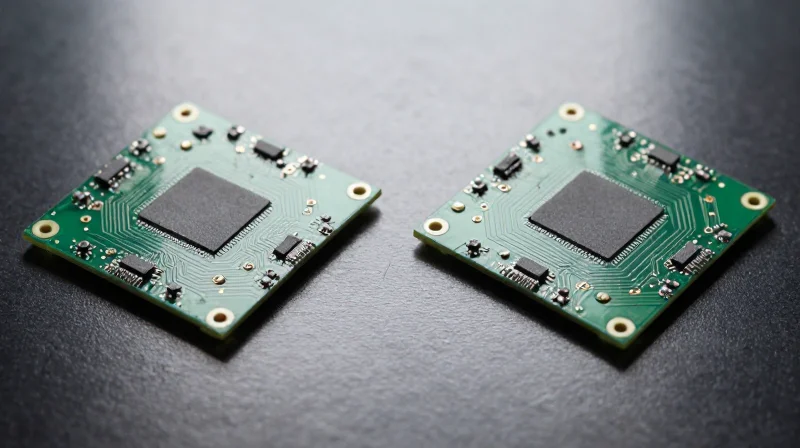
Comparative Fabrication Standards in Space Environments
The choice between standard commercial-grade fabrication and high-reliability aerospace-certified manufacturing represents the single most significant decision in controlling satellite mission lifecycle costs. While standard PCBs offer lower upfront capital expenditure, they often succumb to the thermal and radiative stresses of LEO (Low Earth Orbit) and GEO (Geosynchronous Earth Orbit), leading to mission-critical failures that invalidate initial cost savings.
| Metric | Standard Fabrication | High-Reliability Fabrication |
|---|---|---|
| Failure Rate (MTBF) | High (Thermal Cycling Stress) | Low (Resilient Interconnects) |
| Inspection Rigor | Visual/AOI Only | X-Ray/Microsectioning |
| Total Cost of Ownership | High (Replacement/Redundancy) | Low (Long-Term Mission Success) |
Analyzing the ROI Impact of Fabrication Quality
High-reliability fabrication utilizes specialized processes—such as controlled depth drilling, stringent copper plating thickness requirements, and advanced surface finishes—to ensure integrity. By minimizing interconnect fatigue, operators effectively eliminate the latent failure modes that necessitate premature mission termination.
- How does PCB failure manifest in orbit?
Failures typically appear as delamination or fractured solder joints due to extreme coefficients of thermal expansion (CTE) mismatches during orbit transitions, leading to intermittent signal loss. - Does high-reliability fabrication increase lead times?
While additional validation steps increase production time, this delay is negligible when weighed against the risk of hardware failure, which can result in the loss of a multi-million dollar satellite asset. - Is the TCO (Total Cost of Ownership) lower for aerospace-grade boards?
Yes. The premium paid for enhanced fabrication is offset by the elimination of expensive ground-station troubleshooting, increased data throughput consistency, and the avoidance of redundant mission hardware.
Thermal Management and PCB Longevity
The Thermal-Mechanical Nexus in Space
In the vacuum of space, convection is non-existent, making conductive heat dissipation the primary mechanism for protecting mission-critical hardware. High-frequency PCBs, which often host power-dense RF components, face extreme thermal gradients that threaten board integrity. By optimizing the copper weight, layer stackup, and the integration of thermal vias, engineers can create a low-impedance thermal path that wicks heat away from sensitive junctions to the chassis, significantly extending the mean time between failures (MTBF).
Thermal Performance Strategies
| Strategy | Mechanism | ROI Impact |
|---|---|---|
| High-Tg Laminates | Resists softening at elevated temps | Prevents delamination and via fatigue |
| Copper Inlays | Direct thermal grounding | Optimizes heat transfer in localized hotspots |
| Thermal Vias | Vertical heat conduction | Reduces junction temperatures by 15-20% |
FAQs on Thermal Management for Satellite PCBs
- How do thermal vias impact signal integrity in high-frequency boards?
While essential for cooling, thermal vias can introduce impedance discontinuities. Precision fabrication processes—such as back-drilling and optimized pattern layout—are used to mitigate parasitic capacitance, ensuring thermal relief does not compromise high-frequency signal performance. - Why is the Coefficient of Thermal Expansion (CTE) so critical for LEO missions?
LEO satellites endure rapid thermal cycling as they transition between sunlight and shadow. If the PCB materials and component packages have mismatched CTEs, repeated expansion and contraction can lead to solder joint cracking, necessitating robust, flexible material choices.
Streamlining the Supply Chain for Mission Success
Strategic Partner Selection for Aerospace Integrity
Streamlining the satellite supply chain hinges on the shift from transactional vendor relationships to collaborative partnerships with fabricators deeply embedded in aerospace standards. By integrating quality assurance protocols early in the design cycle, mission teams can mitigate the risks associated with material inconsistency, supply gaps, and suboptimal board performance in harsh vacuum environments.
| Selection Criteria | Standard Fabricator | Aerospace-Grade Partner |
|---|---|---|
| Quality Certification | ISO 9001 only | AS9100 Rev D & MIL-PRF-31032 |
| Material Sourcing | Off-the-shelf catalog | Validated aerospace-grade polymers |
| Traceability | Lot-level documentation | Full digital pedigree/material tracking |
| Failure Analysis | Basic visual inspection | In-house SEM and thermal cycling tests |
Mitigating Procurement Risks in High-Frequency PCB Design
Supply chain disruption often stems from material variability. Precision RF circuits, particularly those operating in Ka and V bands, are hyper-sensitive to dielectric constant (Dk) fluctuations. Selecting a partner that performs incoming material characterization ensures that the raw laminates meet the stringent simulation parameters before fabrication begins, preventing wasted production cycles.
- How does early involvement of a manufacturer affect ROI?
Early Design for Manufacturing (DFM) input identifies potential routing or material issues that could cause signal degradation, preventing expensive board-level failures and rework later in the assembly phase. - What is the primary benefit of audited supply chains?
Audited chains ensure that materials, such as high-frequency PTFE laminates, are not counterfeited and have been stored under optimal environmental conditions, which is crucial for preventing delamination during thermal cycling in space. - Why is material validation critical for satellite PCBs?
Material validation prevents 'batch drift' where different production lots exhibit variance in impedance; for high-frequency satellite communication, even minor variances can cause significant data packet loss.
Future-Proofing Your Satellite Constellation
Architecting for Scalability and Orbital Longevity
To maximize Return on Investment (ROI) over extended mission lifespans, satellite operators must move beyond baseline aerospace standards. By integrating advanced substrate materials—such as low-loss PTFE-based laminates and high-Tg resins—manufacturers can create PCB architectures capable of withstanding the thermal cycling, radiation exposure, and vacuum conditions inherent in LEO and MEO orbits. Future-proofing is achieved not by replacing hardware, but by selecting materials and manufacturing tolerances that prevent degradation over a 7-to-10-year operational life.
Comparative Strategic Advantages
| Investment Criteria | Baseline Fabrication | Future-Proofed Fabrication |
|---|---|---|
| Material Thermal Stability | Moderate (High risk of delamination) | Superior (High Tg, CTE matching) |
| Frequency Bandwidth | Fixed/Static | Broadband/Adaptable |
| Life-Cycle ROI | Low (Frequent replacement cost) | High (Extended mission capability) |
Key Considerations for Future-Ready Design
- How do material choices influence multi-year mission ROI?
Selecting high-frequency laminates with stable dielectric constants (Dk) ensures signal integrity remains constant as boards age, avoiding the need for aggressive transmission power compensation which depletes onboard batteries. - Why prioritize precision interconnect technology?
Micro-via integrity and advanced plating processes mitigate the risk of thermal fatigue at connection points, which is a primary cause of hardware failure in high-frequency RF modules. - Can current PCB designs scale for future payload updates?
Designing with modular footprint flexibility and high-density interconnect (HDI) allows for faster integration of upgraded SDRs or sensors without necessitating a full redesign of the satellite's core bus.
Ultimately, the cost of high-precision PCB manufacturing is a fraction of total launch and operational costs. Investing in superior board-level reliability at the fabrication stage acts as a hedge against the immense financial impact of satellite downtime or mission failure, securing the constellation's utility well into the next decade.
When mission success depends on the flawless performance of thousands of orbiting nodes, the quality of your PCBs is the single most critical variable. By prioritizing precision, material integrity, and rigorous fabrication standards, your organization can avoid the catastrophic costs of premature failure and ensure optimal operational lifespan. Contact our aerospace engineering team today to audit your current PCB strategy and learn how to optimize your next mission for maximum ROI.
