In the relentless pursuit of faster, more reliable, and higher-capacity data transmission, microwave link converters stand as critical components. These sophisticated devices are the backbone of modern communication infrastructure, from telecommunications and satellite communication to advanced radar systems. Yet, their performance hinges significantly on the underlying Printed Circuit Board (PCB) technology. At Zero One Solution Limited, we understand that a superior PCB solution is not just about manufacturing; it's about enabling innovation and accelerating market entry. As a veteran engineer from Silicon Valley, I've witnessed firsthand the transformative power of expertly crafted PCB solutions. This article delves into how Zero One Solution Limited's Microwave Link Converter PCB Solution is engineered to meet the rigorous demands of high-frequency applications, empowering our clients to push the boundaries of wireless technology.
The Critical Role of PCBs in Microwave Link Converters
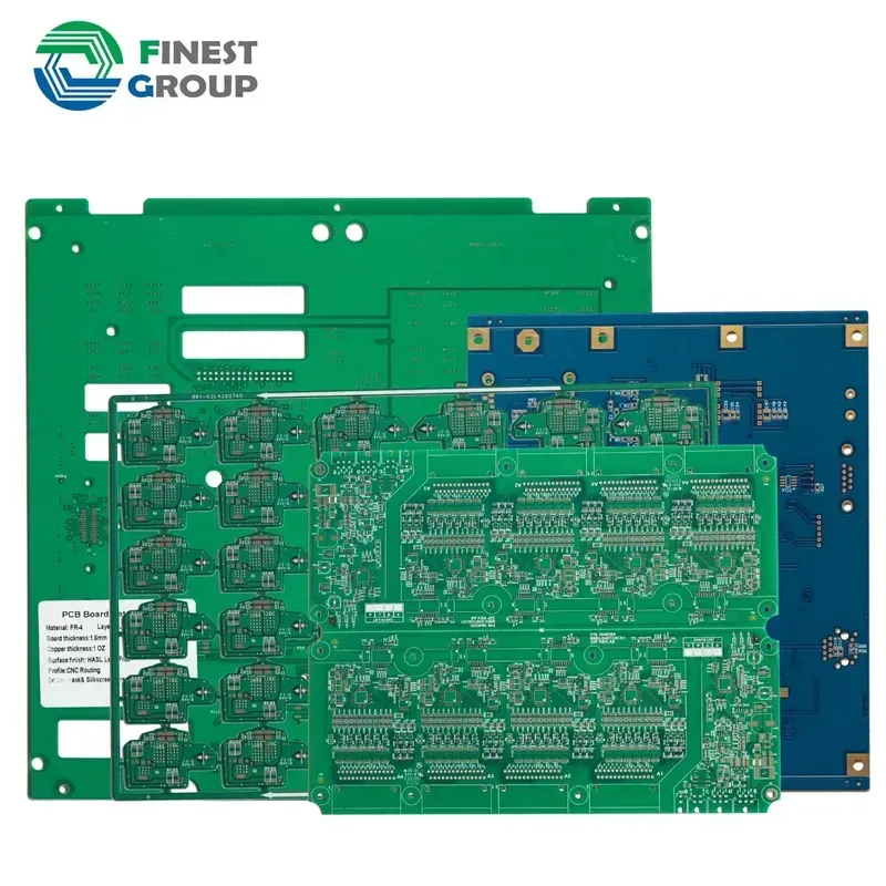
Microwave Link Converter PCB Board
In the demanding realm of wireless communication, Microwave Link Converters serve as the backbone for high-speed data transmission, bridging vast distances with unparalleled efficiency. At the heart of these sophisticated devices lies the Printed Circuit Board (PCB), an often-underestimated component that is, in fact, the foundational element dictating the converter's reliability, performance, and longevity. The unique operational environment of microwave frequencies—typically ranging from 1 GHz to 300 GHz—imposes extraordinary demands on PCB design and manufacturing, transforming a standard circuit board into a highly specialized, precision-engineered platform.
The PCB in a Microwave Link Converter is not merely a conduit for electrical signals; it is an integral part of the RF (Radio Frequency) circuit itself. Its characteristics directly influence signal integrity, impedance matching, power delivery, and thermal dissipation, all of which are critical for maintaining the high-frequency performance required for robust microwave links. Any compromise in the PCB's design, material selection, or manufacturing precision can lead to significant signal loss, reflections, interference, and ultimately, system failure. Therefore, understanding the critical role of these specialized PCBs is paramount for anyone involved in developing, deploying, or maintaining microwave communication infrastructure.
Why are PCBs critical for Microwave Link Converters? PCBs provide the physical and electrical foundation, directly impacting signal integrity, impedance control, thermal management, and power delivery at high frequencies. Their precision is crucial for maintaining performance and preventing signal degradation in microwave applications. Failure to optimize the PCB leads to significant signal loss and system instability, highlighting its foundational role in the overall system's success and reliability.
Key PCB Requirements
Impact on Microwave Link Converter Performance
High-Frequency Signal Integrity
Minimizes signal loss, distortion, and crosstalk, ensuring clear and reliable data transmission over long distances. Essential for maintaining the high data rates characteristic of microwave links. Without it, signal attenuation becomes a major impediment, reducing effective range and throughput, thereby compromising the entire communication link's efficiency and reliability in critical applications like backhaul networks or satellite communications, where even minor signal degradation can have cascading effects on network performance and data integrity across the system and could lead to system outages or data corruption. It ensures that the transmitted signal reaches its destination with minimal degradation, preserving the fidelity and integrity of the data stream, which is particularly vital for applications requiring high bandwidth and low latency, such as 5G infrastructure or secure military communications. Optimized signal paths and controlled impedance are crucial for preventing reflections and standing waves that can severely impact the link's power efficiency and error rate. The design must account for skin effect, dielectric losses, and electromagnetic interference (EMI), employing advanced routing techniques and shielding to maintain signal quality across the entire frequency spectrum utilized by the microwave converter, thereby ensuring robust and consistent operation even in challenging environmental conditions or high-noise scenarios, leading to an increase in network availability and system uptime while reducing the overall operational cost of the infrastructure by minimizing maintenance and troubleshooting efforts over its operational lifespan and enhancing data throughput, enabling the deployment of more reliable and higher-capacity communication networks, which directly supports the growing demands of modern digital economies and enhances the overall efficiency of information exchange across various industries and applications, ultimately contributing to a more connected and technologically advanced society for future communication needs, ensuring a resilient and high-performance communication backbone for the most demanding applications in diverse sectors such as telecommunications, aerospace, and defense.
Challenges in Designing and Manufacturing Microwave Link Converter PCBs
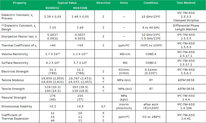
High-Frequency PCB Materials
The development and production of Printed Circuit Boards (PCBs) for microwave link converters present a formidable array of technical hurdles that demand a highly specialized and precise engineering approach. Unlike conventional PCBs, these high-frequency applications operate within a delicate ecosystem where even minor deviations can lead to significant performance degradation. The core challenge lies in maintaining signal integrity across a broad spectrum of frequencies, which necessitates meticulous attention to material science, electromagnetic principles, and advanced manufacturing processes to ensure optimal reliability and efficiency in microwave link converter PCB solutions.
Impedance Matching Precision Achieving precise 50-ohm (or other specified) impedance across all signal paths is paramount in microwave circuits. Mismatched impedance leads to signal reflections, power loss, and distortion, significantly impacting the converter's efficiency and data throughput. This requires careful trace width calculation, dielectric constant consistency, and precise stack-up design.
Minimizing Signal Loss At microwave frequencies, conductor losses (skin effect), dielectric losses (tangent delta), and radiation losses become pronounced. Selecting ultra-low-loss dielectric materials (e.g., PTFE, high-frequency laminates like Rogers, Taconic) and optimizing trace geometries are critical to mitigate attenuation and maintain signal strength over the transmission path.
Effective Thermal Management High-frequency components generate significant heat, which can degrade performance and reliability. Designing effective thermal dissipation pathways through copper pours, thermal vias, and strategic component placement is crucial. The thermal conductivity of the PCB material itself also plays a vital role in preventing hot spots and ensuring long-term operational stability.
Material Selection Complexity The choice of PCB substrate is a critical differentiator. Standard FR-4 is often inadequate due to its higher dielectric loss tangent and inconsistent dielectric constant at microwave frequencies. Specialized low-loss, stable dielectric materials are essential, but they often come with higher costs and require specific manufacturing expertise for processing.
Stringent Manufacturing Tolerances Fabricating microwave PCBs demands exceptionally tight manufacturing tolerances. Variations in trace width, spacing, copper thickness, and dielectric thickness, which might be acceptable for lower-frequency boards, can severely impact impedance control and signal integrity at microwave frequencies. This requires highly precise etching, drilling, and lamination processes.
Crosstalk and EMI Mitigation The dense packing of high-frequency traces on a PCB can lead to unwanted coupling (crosstalk) and electromagnetic interference (EMI). Advanced layout techniques, including proper ground plane design, shielding, isolation, and strategic component placement, are necessary to minimize these effects and ensure signal purity.
Reliability and Durability in Harsh Environments Microwave link converters often operate in challenging outdoor or industrial environments. The PCB must withstand temperature extremes, humidity, vibration, and other environmental stressors. This necessitates robust design, appropriate surface finishes (e.g., ENIG for superior solderability and reliability), and stringent quality control during manufacturing to ensure long-term durability.
Zero One Solution Limited's Comprehensive Microwave PCB Solution
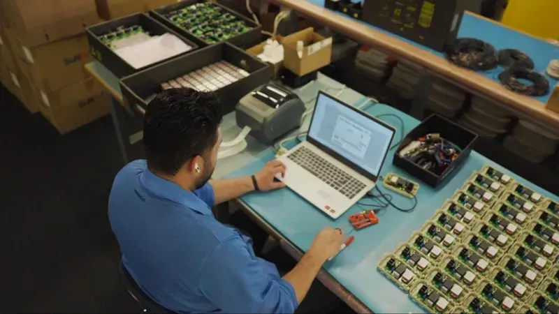
PCB Design Engineer at Work
At Zero One Solution Limited, we recognize that the demanding nature of Microwave Link Converters necessitates a truly comprehensive PCB solution, moving beyond mere manufacturing to encompass the entire product lifecycle. Our holistic approach directly addresses the intricate challenges of high-frequency design, material science, and precision fabrication, ensuring that every PCB we deliver for your microwave link converter applications exhibits unparalleled signal integrity and robust performance. We empower innovation by providing a seamless, end-to-end service that transforms your complex specifications into high-reliability, high-performance printed circuit boards.
End-to-End Service Portfolio for Microwave Link Converter PCBs We offer a fully integrated suite of services, from initial concept to final assembly, ensuring continuity and consistency. This includes expert design consultation, meticulous material selection, rapid prototyping, advanced manufacturing, and precise assembly, all optimized for high-frequency applications like microwave link converters. This comprehensive model minimizes vendor fragmentation and accelerates your development cycle.
Specialized High-Frequency PCB Design Expertise Our veteran engineering team, with decades of Silicon Valley experience, excels in high-frequency PCB layout. We employ advanced simulation tools and deep knowledge of impedance control, crosstalk mitigation, and signal loss minimization to guarantee optimal performance for microwave frequencies. This expertise is critical in mitigating signal degradation, a common pain point in microwave link converter designs.
Strategic Material Selection for Optimal Performance The choice of substrate is paramount for microwave PCBs. We advise on and procure the most suitable low-loss dielectric materials (e.g., PTFE, ceramic-filled laminates) that offer stable dielectric constant (Dk) and dissipation factor (Df) across a wide range of temperatures and frequencies. This ensures your microwave link converter PCBs maintain performance under diverse operational conditions.
Rapid Prototyping and Iteration Support Our core strength in rapid-response R&D prototype manufacturing significantly shortens your time-to-market. We provide quick-turn prototypes with uncompromising quality, enabling agile design iteration and validation. This capability is invaluable for fine-tuning complex microwave link converter designs before mass production, reducing risks and costs.
Advanced Manufacturing and Assembly Capabilities Leveraging state-of-the-art facilities in Shenzhen and a global supply chain, we execute precision manufacturing processes including fine-line etching, multi-layer stack-up management, and advanced surface finishes. Our assembly services are tailored for high-frequency components, ensuring precise placement and soldering, vital for the reliability of microwave link converter PCBs.
Advanced Technologies for High-Frequency PCB Manufacturing
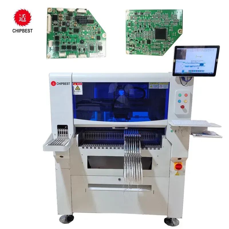
Precision PCB Manufacturing Equipment
Manufacturing high-frequency PCBs for microwave link converters demands cutting-edge technologies and meticulous processes to ensure unparalleled signal integrity, minimal loss, and robust performance. At Zero One Solution Limited, we leverage state-of-the-art manufacturing techniques and advanced material science to overcome the inherent challenges of gigahertz frequencies, delivering reliable and high-performance PCB solutions critical for modern wireless communication infrastructure.
Precision Etching and Trace Definition Achieving sub-micron trace width and spacing accuracy is paramount for impedance control in microwave circuits. We employ advanced direct imaging and laser-drilling technologies, coupled with highly controlled chemical etching processes, to fabricate precise transmission lines (e.g., microstrip, stripline, coplanar waveguide) that maintain consistent impedance and minimize signal reflections at high frequencies. This precision is vital for the optimal performance of microwave link converters, where even minor deviations can lead to significant signal degradation.
Multi-Layer Stack-up Optimization for RF Performance Our expertise extends to designing and manufacturing complex multi-layer PCB stack-ups specifically optimized for high-frequency applications. This involves strategic placement of ground planes, power planes, and signal layers, along with careful selection of dielectric materials with stable dielectric constants (Dk) and low dissipation factors (Df). Our engineers meticulously simulate and validate stack-up configurations to mitigate crosstalk, improve EMI/EMC performance, and ensure thermal stability, all crucial for the sustained reliability of microwave link converter PCBs.
Technology Aspect
Benefit for Microwave Link Converters
Zero One Solution Limited's Approach
Material Selection
Reduced signal loss, stable performance across temperature and frequency
Utilizes low-loss dielectrics like Rogers, Arlon, Isola with precise Dk/Df control
Advanced Surface Finishes
Enhanced signal integrity, superior solderability, long-term reliability
Offers ENIG (Electroless Nickel Immersion Gold), Immersion Silver, and OSP tailored for high-frequency pads and fine-pitch components
Impedance Control
Minimizes signal reflections, ensures efficient power transfer
Strict +/- 5% impedance tolerance through sophisticated design tools and TDR testing
Incorporates thermal vias, metal core PCBs, and heatsink integration for optimal heat dissipation
Quality Control
Ensures consistent performance, compliance with industry standards
IPC Class 2/3 compliant, automated optical inspection (AOI), X-ray inspection, and comprehensive RF testing
Our commitment to these advanced manufacturing technologies ensures that every Microwave Link Converter PCB solution we deliver not only meets but often exceeds the stringent performance and reliability requirements of the telecommunications industry. This meticulous approach, from material selection to final quality checks, underpins the superior functionality of your microwave link converter products.
Rapid Prototyping: Accelerating Your Innovation Cycle
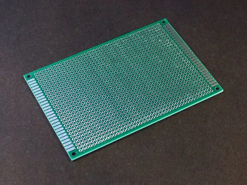
PCB Prototype Board
In the fast-paced realm of microwave link converter development, speed to market is paramount. Zero One Solution Limited's rapid prototyping capabilities are specifically engineered to provide a critical competitive advantage, enabling our clients to dramatically accelerate their innovation cycles. We understand that quick, high-fidelity iterations are essential for validating designs, mitigating risks, and ultimately bringing advanced microwave solutions to market faster than competitors. Our streamlined processes and dedicated resources ensure that your visionary concepts are transformed into functional prototypes with unparalleled efficiency.
Reduced Time-to-Market Our rapid prototyping services drastically cut down the time required from design conception to functional PCB prototype, often by weeks or even months compared to traditional methods. This allows for earlier product launches and increased market share for your microwave link converters.
Iterative Design Optimization The ability to quickly produce multiple prototype iterations empowers engineers to test, analyze, and refine designs with unmatched agility. This iterative approach is crucial for optimizing signal integrity, thermal performance, and overall reliability in complex microwave circuits.
Cost Efficiency in Development While speed is key, our rapid prototyping also contributes to cost efficiency by identifying design flaws early in the development cycle. Rectifying issues at the prototype stage is significantly less expensive than discovering them during mass production, saving substantial resources.
Our commitment to rapid prototyping is underpinned by advanced manufacturing technologies and an agile operational framework. From initial Gerber file submission to final prototype delivery, every step is optimized for speed without compromising the stringent quality requirements of microwave link converter PCBs. This includes expedited material sourcing for specialized high-frequency laminates, dedicated production lines for quick-turn projects, and accelerated quality assurance protocols. By partnering with Zero One Solution Limited, you gain access to a robust prototyping ecosystem designed to transform your R&D pipeline into a rapid innovation engine, ensuring your microwave link converters are at the forefront of technological advancement.
One-Stop Service: From Design to Assembly
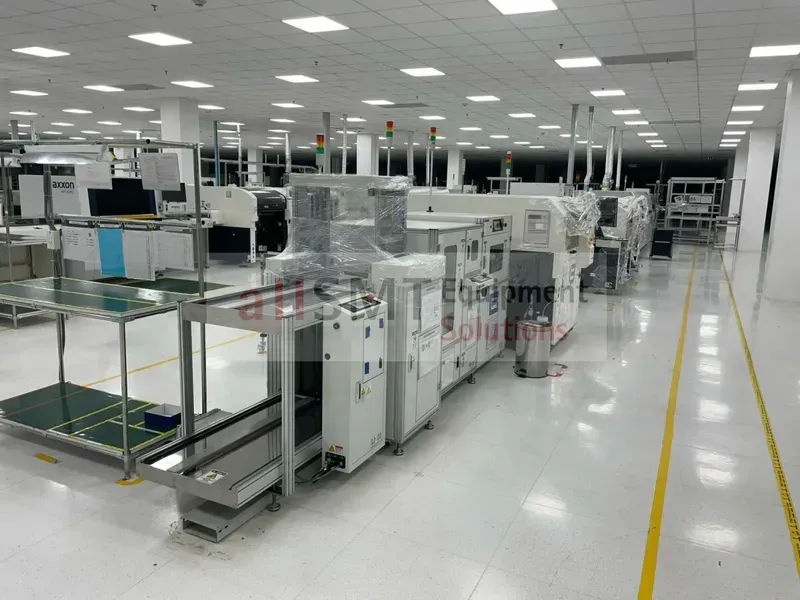
PCB Assembly Production Line
At Zero One Solution Limited, we understand that product development is a multifaceted process that demands seamless integration and exceptional quality at every stage. Our 'One-Stop Service' for Microwave Link Converter PCB solutions is meticulously designed to eliminate the complexities and inefficiencies often associated with managing multiple vendors, offering a streamlined, comprehensive pathway from initial concept to final assembly. This integrated approach not only accelerates your project timelines but also guarantees consistent quality and performance across the entire PCB lifecycle, which is paramount for the high-frequency demands of microwave link converters.
Integrated Design and Engineering Consultation Our service begins with expert design consultation, where our veteran engineers collaborate closely with your team to optimize the PCB layout for high-frequency performance, impedance matching, and thermal management specifically for microwave link converters. We leverage advanced simulation tools to ensure design integrity before manufacturing commences.
Strategic Material Procurement and Management Access to high-quality, specialized materials is critical for microwave PCBs. We handle the entire procurement process, sourcing low-loss dielectric substrates (e.g., Rogers, Arlon) and other crucial components from a globally vetted supply chain. Our strategic location in Shenzhen, China's electronic manufacturing hub, and our Dubai branch office provide unparalleled access to a diverse and reliable network of suppliers.
Precision Manufacturing and Fabrication With state-of-the-art facilities, we employ advanced manufacturing processes including precision etching, multi-layer stack-up optimization, and specialized surface finishes (e.g., ENIG, Immersion Silver) tailored for the rigorous demands of microwave frequencies. Our stringent quality control measures ensure every PCB meets the exact specifications for your converter applications.
Advanced Component Assembly (PCBA) Beyond bare board fabrication, our one-stop solution extends to high-precision PCB assembly. We are equipped for both SMT and THT assembly, handling sensitive microwave components with utmost care. Our automated assembly lines ensure accuracy and efficiency, critical for complex microwave link converter boards, followed by thorough testing to validate functionality.
Rigorous Quality Assurance and Testing Quality is embedded at every step. From incoming material inspection to in-process checks and final functional testing, we implement a multi-stage quality assurance protocol. For microwave link converter PCBs, this includes specialized RF testing to verify signal integrity, return loss, and insertion loss, ensuring optimal performance in the field.
By consolidating all critical stages—from design and material sourcing to manufacturing and assembly—under one roof, Zero One Solution Limited significantly reduces lead times, minimizes communication overheads, and provides unparalleled accountability. This integrated approach ensures that your Microwave Link Converter PCB solutions are not only delivered rapidly but also with the highest standards of quality and performance, giving you a distinct competitive edge in the market.
Why Choose Zero One Solution Limited for Your Microwave Link Converter PCBs?
When the stakes are high, and signal integrity is paramount, selecting the right PCB solution provider for your microwave link converters is not merely a choice—it's a strategic imperative. Zero One Solution Limited stands as a beacon of excellence in this specialized field, offering a compelling blend of experience, advanced capabilities, and unwavering commitment to quality that ensures your high-frequency designs achieve peak performance and reliability. Our comprehensive approach, from rapid prototyping to one-stop manufacturing and assembly, is specifically tailored to meet the rigorous demands of microwave applications.
Decade-Plus of Specialized Experience With over a decade of dedicated expertise in PCB solutions, Zero One Solution Limited has cultivated a deep understanding of the intricacies involved in high-frequency circuit board design and manufacturing. Our extensive track record is particularly strong in demanding applications such as microwave link converters, where precision and performance are non-negotiable. This long-standing experience translates into robust, reliable PCBs that meet the highest industry standards.
Silicon Valley Veteran Engineering Acumen Our team is fortified by veteran engineers with extensive experience garnered from Silicon Valley's most competitive environments. This elite engineering prowess ensures that every PCB design and manufacturing process benefits from cutting-edge methodologies, innovative problem-solving, and a forward-thinking approach to high-frequency challenges, guaranteeing superior signal integrity and system performance for your microwave link converters.
Strategic Global Footprint for Seamless Supply Headquartered in Shenzhen, China – the global hub of electronics manufacturing – and complemented by a branch office in Dubai, Zero One Solution Limited commands a strategically advantageous global presence. This dual-location model ensures not only efficient access to the world's most advanced manufacturing ecosystems but also provides flexible, responsive support and logistics, optimizing your supply chain for microwave link converter PCB production.
Uncompromised Commitment to Quality and Performance Quality is the cornerstone of our operations. We adhere to stringent quality control protocols and utilize advanced manufacturing technologies, including precision etching and optimized multi-layer stack-ups, specifically designed for high-frequency PCBs. Our meticulous approach guarantees that each board for your microwave link converter is fabricated to exact specifications, delivering exceptional electrical characteristics and long-term reliability.
Accelerated Innovation through Rapid Prototyping Understanding the critical importance of time-to-market, our rapid prototyping capabilities are a distinct competitive advantage. We empower clients to quickly iterate on designs and validate concepts, significantly reducing development cycles for microwave link converter products. This agility ensures that your innovative solutions can reach the market faster, gaining crucial early-mover advantages.
Integrated One-Stop Service Efficiency From initial design consultation and material selection to rapid prototyping, manufacturing, and final assembly, Zero One Solution Limited offers a seamless 'one-stop' service. This integrated approach simplifies project management, minimizes coordination complexities, and ensures consistent quality across every stage of your microwave link converter PCB production, allowing you to focus on core product development.
FAQs About Microwave Link Converter PCB Solutions
What are the primary considerations for PCB material selection in microwave link converters? The primary considerations for PCB material selection in microwave link converters are dielectric constant (Dk), dissipation factor (Df), thermal expansion (CTE), and stability across frequency and temperature. Low Dk materials, such as PTFE-based laminates (e.g., Rogers, Arlon), are crucial for maintaining signal integrity and impedance control at microwave frequencies, minimizing signal loss and ensuring optimal performance. A low Df is equally important to reduce power loss, particularly critical in high-power applications. CTE matching with component lead frames helps prevent solder joint failures over thermal cycling. Zero One Solution Limited rigorously evaluates these parameters to select the ideal material for each unique microwave link converter design, ensuring long-term reliability and superior performance.
How does Zero One Solution Limited ensure signal integrity in high-frequency microwave link converter PCBs? Zero One Solution Limited ensures signal integrity in high-frequency microwave link converter PCBs through a multi-faceted approach. This includes precise impedance control, achieved via accurate trace width and spacing calculations and validated by TDR measurements. We utilize advanced stack-up design, employing differential pairs and ground planes to minimize crosstalk and electromagnetic interference (EMI). Furthermore, meticulous component placement, optimized routing geometries with minimal vias, and the use of low-loss dielectric materials are integral to preserving signal quality and minimizing attenuation across the operational bandwidth of microwave link converters. Our engineering team employs simulation tools to predict and mitigate signal integrity issues before manufacturing.
What specific manufacturing processes are critical for microwave link converter PCB reliability? For microwave link converter PCB reliability, critical manufacturing processes include high-precision etching for tight impedance tolerances, advanced multi-layer lamination for consistent dielectric thickness and layer registration, and specialized surface finishes like Electroless Nickel Immersion Gold (ENIG) or Immersion Silver. These finishes offer superior solderability, flatness, and shelf life, which are essential for fine-pitch components and robust solder joints. Additionally, stringent quality control measures, including AOI, X-ray inspection, and comprehensive electrical testing (e.g., TDR, S-parameter measurements), are implemented at every stage to ensure the board meets the rigorous performance specifications required for microwave applications.
How does thermal management impact the performance of microwave link converter PCBs? Thermal management significantly impacts the performance and longevity of microwave link converter PCBs. Excessive heat can degrade active components, alter material properties, and increase signal loss. Zero One Solution Limited addresses this through strategic design elements such as thermal vias, optimized copper pours for heat dissipation, and careful component placement to distribute thermal loads. We also consider board materials with higher thermal conductivity and, where necessary, integrate heat sinks or active cooling solutions. Effective thermal management ensures stable electrical performance, prevents frequency drift, and extends the operational life of the microwave link converter, especially in high-power or challenging environmental conditions.
Why is rapid prototyping essential for developing microwave link converter solutions? Rapid prototyping is essential for developing microwave link converter solutions because it significantly accelerates the design-validation-iteration cycle. Microwave frequencies are highly sensitive to physical layout, and theoretical models often require real-world validation. Rapid prototyping allows engineers to quickly test PCB designs, identify and resolve issues related to signal integrity, impedance matching, thermal performance, and overall functionality. This iterative process minimizes costly redesigns, reduces time-to-market, and enables faster innovation, giving our clients a crucial competitive edge in the fast-paced telecommunications industry. Zero One Solution Limited's rapid prototyping capabilities are designed to meet these urgent development needs.
What makes Zero One Solution Limited a preferred partner for Microwave Link Converter PCB Solutions? Zero One Solution Limited is a preferred partner for Microwave Link Converter PCB Solutions due to our specialized expertise, comprehensive one-stop services, and strategic global presence. With over a decade of experience and a team of veteran Silicon Valley engineers, we possess deep knowledge in high-frequency PCB design and manufacturing. Our end-to-end services, from design to assembly, streamline the entire production process, ensuring consistent quality and efficiency. Our rapid prototyping capabilities accelerate product development, while our strategic locations in Shenzhen and Dubai ensure seamless access to resources and global supply chains, providing unparalleled support and competitive advantages for our clients.
In conclusion, the efficacy of microwave link converters is inextricably linked to the precision and performance of their PCB foundation. Zero One Solution Limited's Microwave Link Converter PCB Solution is a testament to our commitment to excellence, offering unparalleled expertise from design to assembly. Our rapid prototyping capabilities and one-stop service model ensure that your innovative concepts transition seamlessly from drawing board to market. With our strategic global presence and deep understanding of high-frequency challenges, we are not just a supplier; we are your dedicated partner in innovation. Ready to accelerate your next-generation microwave link project? Contact Zero One Solution Limited today to discover how our comprehensive PCB solutions can empower your success.