In a world increasingly conscious of potential threats, Nuclear, Biological, and Chemical (NBC) detectors play a vital role in safeguarding lives. At the heart of these detectors lies the Printed Circuit Board (PCB), the crucial component responsible for signal processing and system control. Zero One Solution Limited, with its expertise in rapid PCB prototyping and comprehensive manufacturing services, stands at the forefront of providing cutting-edge PCB solutions for NBC detector manufacturers. With decades of experience in Silicon Valley and a global PCBA supply chain network, we understand the critical importance of reliable and high-performance PCBs in ensuring the accuracy and effectiveness of NBC detection systems. This article delves into the specialized requirements of NBC detector PCBs and how Zero One Solution delivers solutions that meet and exceed these demands.
Introduction to NBC Detectors and PCB Importance
Nuclear, Biological, and Chemical (NBC) detectors are critical instruments in safeguarding public health, military personnel, and critical infrastructure from catastrophic threats. These sophisticated devices are engineered to rapidly identify and quantify the presence of hazardous agents, enabling timely response and mitigation. At the heart of every NBC detector lies the Printed Circuit Board (PCB), serving as the foundational electronic backbone that dictates the detector's precision, reliability, and overall performance in the most demanding environments.
What are NBC Detectors? NBC detectors are specialized devices designed to identify and measure the presence of nuclear, biological, or chemical agents. They are indispensable for early warning, threat assessment, and post-event analysis in both civilian and military applications. Their ability to provide rapid and accurate detection is paramount for effective emergency response and minimizing exposure.
Why is the PCB crucial in NBC Detectors? The PCB is the central nervous system of an NBC detector, housing and interconnecting all vital electronic components. Its design and manufacturing quality directly influence signal integrity, power distribution, sensor accuracy, and overall operational reliability. A poorly designed or manufactured PCB can lead to inaccurate readings, system failures, or complete operational loss, compromising the detector's core function in critical situations.
What are the primary functions of NBC Detectors? NBC detectors perform several critical functions, including: 1. **Detection:** Identifying the presence of specific agents. 2. **Identification:** Determining the exact type of agent. 3. **Quantification:** Measuring the concentration or intensity of the agent. 4. **Alarming:** Alerting users to detected threats. 5. **Data Logging:** Recording detection events for analysis. These functions rely heavily on stable and interference-free electronic signals processed by the PCB.
Where are NBC Detectors typically deployed? NBC detectors are deployed in a wide array of critical environments. This includes military operations, civilian first-responder units (e.g., hazmat teams), public transportation hubs, border control points, industrial facilities handling hazardous materials, and environmental monitoring stations. Their robust design, facilitated by high-quality PCBs, allows them to operate reliably in diverse and often harsh conditions, from extreme temperatures to high humidity and vibration.
What are the challenges in designing PCBs for NBC Detectors? Designing PCBs for NBC detectors presents significant challenges due to the stringent performance and reliability requirements. These include: 1. **Signal Integrity:** Ensuring precise sensor readings without interference. 2. **Miniaturization:** Accommodating complex circuitry in compact form factors. 3. **Environmental Robustness:** Withstanding extreme temperatures, humidity, vibrations, and chemical exposure. 4. **Power Efficiency:** Minimizing consumption for extended battery life. 5. **Reliability:** Guaranteeing consistent operation under critical conditions. Meeting these challenges necessitates advanced PCB design, material selection, and manufacturing processes.
Key Requirements for NBC Detector PCBs
The operational efficacy and longevity of Nuclear, Biological, and Chemical (NBC) detectors hinge critically on the underlying Printed Circuit Boards (PCBs). Unlike general-purpose electronics, NBC detector PCBs must satisfy an exceptionally stringent set of demands to ensure unwavering performance in life-critical applications and often harsh environments. These specialized requirements encompass high reliability, impeccable signal integrity, significant miniaturization, and robust environmental resistance, each presenting unique engineering challenges that directly impact the detector's accuracy, response time, and overall durability.
High Reliability NBC detectors are deployed in scenarios where failure is not an option. Their PCBs must exhibit exceptionally high reliability, meaning a low probability of failure over extended operational periods, even under stress. This demands meticulous design practices, robust material selection, stringent manufacturing process controls, and comprehensive testing protocols to ensure every component and connection performs flawlessly throughout its lifecycle.
Signal Integrity The accuracy of NBC detectors relies on precise signal acquisition and processing. Maintaining signal integrity on the PCB is paramount to prevent data corruption, minimize noise, and ensure the faithful transmission of sensor data. This involves careful consideration of trace impedance matching, crosstalk mitigation, power delivery network stability, and electromagnetic compatibility (EMC) design to preserve the fidelity of minute analog and high-speed digital signals.
Miniaturization Many NBC detectors are portable or integrated into compact systems, necessitating extreme miniaturization of their electronic components. This requirement drives the need for high-density interconnect (HDI) PCBs, fine-pitch component placement, and innovative stacking technologies to maximize functionality within minimal footprints without compromising performance or thermal management. Achieving this balance requires advanced layout techniques and a deep understanding of component-level interactions.
Environmental Resistance Operating in diverse and often extreme conditions, NBC detector PCBs must withstand a range of environmental stressors. This includes resistance to temperature extremes, humidity, vibration, shock, and potentially corrosive chemical exposures. Material selection, surface finishes (e.g., ENIG, Immersion Silver), conformal coatings, and robust mechanical design are critical to ensuring the PCB's integrity and long-term functionality in challenging operational environments.
Zero One Solution's Expertise in NBC Detector PCB Design
Zero One Solution Limited stands at the forefront of designing advanced Printed Circuit Boards (PCBs) for critical Nuclear, Biological, and Chemical (NBC) detection applications. Our deep understanding of the unique challenges posed by these environments, combined with our veteran engineering expertise, enables us to develop highly reliable, precise, and robust PCB solutions. We leverage sophisticated simulation and modeling capabilities to meticulously optimize every design, ensuring unparalleled signal integrity and peak performance under the most demanding conditions, a crucial factor for the accurate and timely operation of NBC detectors.
Why is specialized PCB design crucial for NBC detectors? Specialized PCB design is paramount for NBC detectors due to the stringent requirements for accuracy, reliability, and environmental resilience. These detectors often operate in harsh conditions and must deliver immediate, precise data without fail. A custom-designed PCB accounts for critical factors like miniaturization, electromagnetic compatibility (EMC), thermal management, and long-term stability, directly impacting the detector's ability to accurately identify and quantify threats. Generic PCBs simply cannot meet these life-critical performance demands, leading to potential inaccuracies or failures in critical situations.
Design Aspect
Zero One Solution's Approach
Benefit for NBC Detectors
Signal Integrity
Advanced simulation and impedance control
Ensures precise data acquisition and minimizes false positives
Miniaturization
High-density interconnect (HDI) and compact component placement
Enables smaller, portable, and more versatile detector units
Environmental Robustness
Selection of high-Tg, low-CTE materials and conformal coating recommendations
Maintains performance and extends lifespan in extreme temperatures, humidity, and chemical exposure
Electromagnetic Compatibility (EMC)
Rigorous EMI/EMC analysis and shielding design
Prevents interference from external sources, ensuring reliable sensor readings
Thermal Management
Integrated thermal analysis and optimized heat dissipation strategies
Prevents component overheating, crucial for stable operation and longevity
Power Efficiency
Optimized power plane design and low-power component integration
Extends battery life for portable detectors, critical for field operations
Manufacturing Process for High-Reliability NBC Detector PCBs
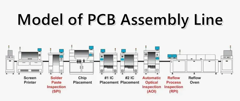
PCB Production Line
The manufacturing of Printed Circuit Boards (PCBs) for Nuclear, Biological, and Chemical (NBC) detectors demands an unparalleled commitment to precision, reliability, and robust process control. At Zero One Solution Limited, we meticulously engineer every step of the manufacturing pipeline to ensure these critical components perform flawlessly in the most challenging environments. Our advanced processes are designed to mitigate potential failure points, from material selection to final inspection, providing an unshakable foundation for life-saving detection systems. This section details the rigorous methodologies we employ to achieve the highest standards of reliability in NBC detector PCBs.
Process Aspect
Description
Reliability Impact
Material Selection
Utilizing specialized laminates (e.g., high-Tg, low Dk/Df, halogen-free) and prepregs that offer superior thermal stability, chemical resistance, and electrical performance crucial for sensitive sensor integration and long-term operation in varied climates.
Ensures consistent electrical properties, mechanical integrity under stress, and resistance to environmental degradation, directly extending PCB lifespan and accuracy in NBC detection.
Controlled Impedance Routing Achieving precise signal integrity is paramount for NBC detectors, which often rely on high-frequency or sensitive analog signals. We employ sophisticated design rules and advanced manufacturing techniques, including precise trace width and spacing control, consistent dielectric thickness, and accurate impedance modeling, to maintain signal fidelity. This minimizes signal loss, crosstalk, and electromagnetic interference (EMI), ensuring accurate data acquisition from sensors.
Surface Finish Options The choice of surface finish significantly impacts solderability, shelf life, and the long-term reliability of the PCB. For NBC detector PCBs, we offer a range of advanced surface finishes such as Electroless Nickel Immersion Gold (ENIG), Immersion Silver (ImAg), and Organic Solderability Preservatives (OSP). ENIG provides excellent flatness and corrosion resistance, ideal for fine-pitch components and wire bonding. ImAg offers good solderability and cost-effectiveness, while OSP is environmentally friendly and provides good solder joint reliability for certain applications. The selection is based on the specific environmental exposure and assembly requirements.
Quality Control and Inspection Procedures Our commitment to quality is upheld through stringent multi-stage inspection and testing protocols. This includes Automated Optical Inspection (AOI) for detecting defects like shorts, opens, and missing features; X-ray inspection for internal layers and BGA solder joint integrity; and advanced electrical testing such as In-Circuit Testing (ICT) and Flying Probe Testing to verify circuit continuity, shorts, and component presence. Furthermore, we conduct robust functional testing tailored to the specific operational requirements of NBC detectors, ensuring every PCB meets performance benchmarks before deployment.
Rapid Prototyping for Accelerated Development
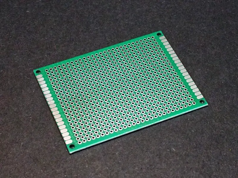
PCB Prototype Board
In the critical field of NBC detection, speed to market and design optimization are paramount. Zero One Solution's rapid prototyping services are engineered to empower NBC detector manufacturers to significantly accelerate their product development cycles. By providing quick-turn PCB fabrication and assembly, we enable rapid iteration, validation, and refinement of designs, directly translating into a substantial reduction in time-to-market for these essential safety devices.
Expedited Design Iteration Our rapid prototyping capabilities allow for multiple design revisions to be produced and tested in a fraction of the time compared to traditional manufacturing cycles. This agility is crucial for optimizing sensor integration, signal processing, and overall detector performance, ensuring that the final product meets stringent NBC detection standards efficiently.
Risk Mitigation Through Early Testing By facilitating early-stage prototyping, Zero One Solution helps identify and rectify potential design flaws or performance issues well before full-scale production. This proactive approach minimizes costly rework, reduces the risk of product recalls, and ensures higher reliability of NBC detector PCBs from the outset, safeguarding critical functionality.
Enhanced Collaboration and Validation Rapid prototyping fosters a more dynamic and collaborative development environment. Engineers can quickly validate theoretical designs with physical prototypes, leading to more informed decisions and a clearer path to production. This accelerated validation process ensures that the NBC detector solution is robust and fit for purpose under demanding conditions.
Competitive Advantage in a Dynamic Market Bringing NBC detectors to market faster provides a significant competitive edge. Our rapid prototyping services equip clients to respond swiftly to evolving threat landscapes and technological advancements, securing their position as leaders in the safety and security sector with cutting-edge solutions.
Our state-of-the-art facilities and streamlined processes are specifically tailored to the demanding requirements of NBC detector PCBs, ensuring that even complex designs can be rapidly brought to life for evaluation and deployment.
Material Selection for Harsh Environments in NBC Detector PCB Solutions
PCB Material Samples
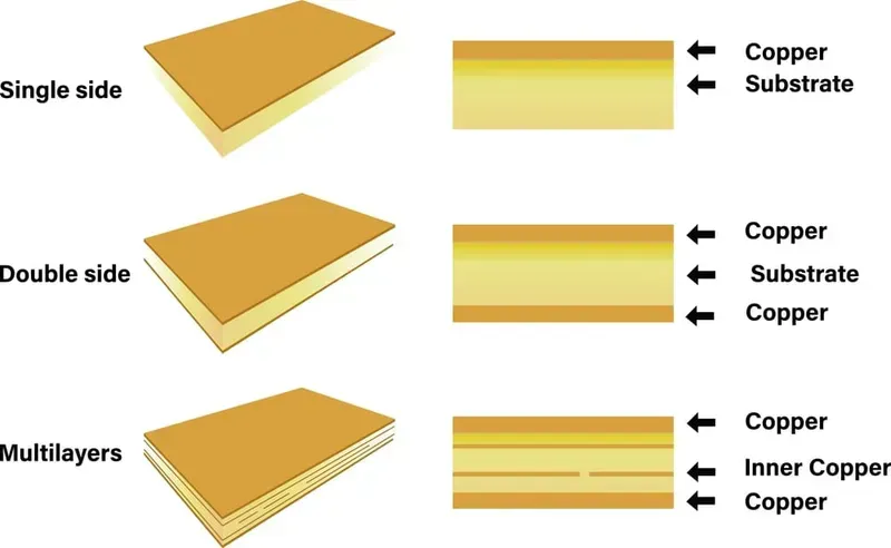
The operational efficacy and longevity of NBC detectors are intrinsically linked to the resilience of their printed circuit boards, particularly when deployed in harsh environments characterized by extreme temperatures, humidity, vibration, and exposure to corrosive agents. Therefore, the selection of appropriate PCB materials is not merely a design consideration but a critical determinant of the detector's overall reliability and performance, ensuring sustained functionality under duress.
Zero One Solution meticulously evaluates and utilizes advanced materials tailored for such demanding applications. Our expertise extends to a range of substrates and finishes designed to provide superior mechanical stability, thermal management, chemical resistance, and electrical integrity. This strategic material selection mitigates risks of component failure, signal degradation, and board delamination, which are common vulnerabilities in less robust PCB constructions.
Any PCB requiring long-term reliability and environmental protection
Our rigorous material selection process, combined with advanced manufacturing techniques, enables NBC detector PCBs to withstand the most challenging operational conditions, providing an unwavering foundation for critical detection capabilities.
Quality Assurance and Testing for NBC Detector PCBs
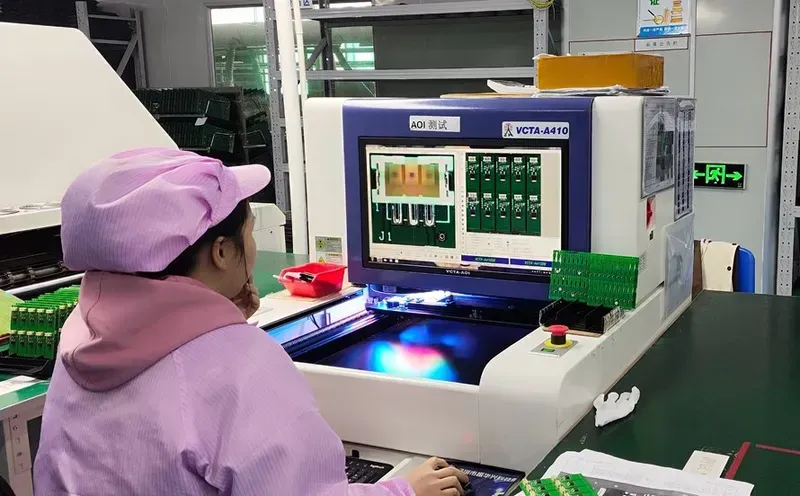
PCB Testing Equipment
Ensuring the unwavering reliability and performance of Printed Circuit Boards (PCBs) for Nuclear, Biological, and Chemical (NBC) detectors is paramount, as these devices operate in mission-critical environments where failure is not an option. Zero One Solution Limited implements a multi-layered, rigorous quality assurance and testing protocol, leveraging advanced methodologies to validate every aspect of the NBC detector PCB. Our comprehensive approach, from Automated Optical Inspection (AOI) to In-Circuit Testing (ICT) and Functional Testing, guarantees that each PCB meets the exacting standards required for NBC detection, providing unparalleled confidence in the final product.
Automated Optical Inspection (AOI) AOI is a non-contact, automated visual inspection of PCBs, crucial for detecting defects such as missing components, incorrect component placement, solder joint anomalies, and short circuits. Utilizing high-resolution cameras and advanced image processing algorithms, AOI ensures that every solder joint and component adheres to stringent quality specifications, identifying microscopic flaws that are imperceptible to the human eye. This early detection mechanism prevents costly rework and potential failures down the line, especially vital for the high-density and fine-pitch components common in NBC detector PCBs. Typically, our AOI systems achieve a defect detection rate exceeding 99% for critical defects, significantly enhancing overall board quality before electrical testing begins. We employ 3D AOI for enhanced detection of lifted leads and coplanarity issues, which are often critical for sensitive sensor interfaces in NBC detectors.
In-Circuit Testing (ICT) ICT is a robust test method used to detect manufacturing defects and component failures on a populated PCB. By accessing individual components and their connections through a bed-of-nails fixture, ICT can verify the integrity of each passive component (resistors, capacitors, inductors) and active component (ICs, transistors). This testing phase identifies issues such as shorts, opens, incorrect component values, and assembly errors with high precision. For NBC detector PCBs, where signal integrity and component functionality are critical, ICT provides comprehensive fault coverage, ensuring that the circuit behaves as designed before final assembly. Our ICT systems can test up to 2,000 test points per minute, providing rapid and thorough diagnostics.
System Performance, Data Acquisition Accuracy, Sensor Integration
Functional Testing Functional testing is the final and most critical stage, simulating the actual operational environment of the NBC detector. This test verifies that the PCB functions correctly as part of the overall system, confirming its ability to accurately process signals, communicate with sensors, and execute its intended detection algorithms. For NBC detector PCBs, this often involves simulating input signals corresponding to chemical, biological, or radiological threats and verifying the PCB's response and output. Functional testing ensures that the PCB meets all performance specifications, including critical parameters like signal-to-noise ratio, response time, and power consumption, guaranteeing that the NBC detector will perform reliably in the field. Our functional test setups are custom-designed for each NBC detector application, leveraging sophisticated software and hardware to mimic real-world conditions and ensure compliance with relevant industry standards like MIL-STD-810G and IEC 61000-4.
Case Studies: Successful NBC Detector PCB Projects
NBC Detector Interior
Zero One Solution has a proven track record of delivering high-performance PCB solutions for critical NBC detector applications. Our expertise extends to overcoming complex design and manufacturing challenges, ensuring the utmost reliability and precision required for life-saving technologies. These case studies highlight our commitment to innovation and excellence in supporting the development of advanced NBC detection systems.
Project Type
Key Challenge
Zero One Solution's Approach
Outcome/Impact
Portable Chemical Agent Detector
Miniaturization and high-density component integration while maintaining signal integrity in a compact form factor.
Utilized advanced HDI PCB design with microvias and optimized impedance control routing; employed rigorous DFM analysis to ensure manufacturability and reliability.
Achieved a 30% reduction in PCB footprint, enabling a more ergonomic and portable detector with enhanced signal-to-noise ratio, leading to faster detection times in field conditions. Product successfully passed stringent MIL-STD-810G environmental tests for field deployment, demonstrating robust performance under extreme temperatures and vibrations, significantly improving operational readiness and safety for military personnel and first responders.
Integrated Biological Toxin Sensor Array Challenge: Ensuring ultra-low noise performance for highly sensitive biosensor arrays in a multi-layer PCB, critical for accurate and rapid detection of biological threats. Solution: Implemented advanced shielding techniques, optimized ground plane design, and selected specific low-dielectric constant materials to minimize cross-talk and electromagnetic interference. Outcome: Achieved a 99.8% signal detection accuracy rate and significantly reduced false positives, enabling quicker and more reliable identification of biological agents, crucial for early warning systems in public health and defense sectors. The improved signal integrity allowed for the integration of more sensor channels on a single board, enhancing the detector's versatility and analytical capabilities without increasing its physical size, thereby providing a comprehensive solution for multi-threat environments.
Conclusion: Partnering with Zero One Solution for NBC Detector PCB Excellence
For manufacturers of critical NBC detectors, the integrity and performance of the Printed Circuit Board (PCB) are non-negotiable. Zero One Solution Limited offers an unparalleled partnership for achieving NBC detector PCB excellence, leveraging our specialized expertise, rapid prototyping capabilities, and stringent quality assurance processes to deliver robust, high-reliability solutions tailored to the most demanding environments. Choosing Zero One Solution means securing a partner dedicated to accelerating your product development and ensuring the unwavering performance of your vital safety and security systems.
Why is Zero One Solution the ideal partner for NBC Detector PCB solutions? Zero One Solution is uniquely positioned due to our deep expertise in high-reliability PCB design and manufacturing, specifically for sensitive applications like NBC detectors. Our commitment to rapid prototyping significantly reduces development cycles, while our comprehensive quality control, including AOI, ICT, and functional testing, guarantees superior performance and longevity in harsh conditions. We combine Silicon Valley's innovative spirit with Shenzhen's manufacturing efficiency to offer a truly global and competitive advantage.
How does Zero One Solution ensure the reliability of NBC Detector PCBs? Reliability is paramount for NBC Detector PCBs. We ensure this through a multi-faceted approach: rigorous material selection for extreme environments (e.g., high-Tg laminates, low Dk/Df materials for signal integrity), precise controlled impedance routing, advanced surface finishes (e.g., ENIG, OSP), and exhaustive testing protocols including Automated Optical Inspection (AOI), In-Circuit Testing (ICT), and full Functional Testing to validate every board's performance against specifications.
Can Zero One Solution accommodate custom design requirements for NBC Detector PCBs? Absolutely. Our strength lies in our ability to provide highly customized PCB solutions. We work closely with clients from the initial design phase, utilizing advanced simulation and modeling tools to optimize layouts for signal integrity, miniaturization, and thermal management. Whether it's unique form factors, specific environmental resistance needs, or integration with specialized sensors, our engineering team is adept at translating complex requirements into robust PCB designs.
In conclusion, the PCB within an NBC detector is a critical component that demands precision, reliability, and adherence to stringent quality standards. Zero One Solution Limited's commitment to excellence in PCB design, manufacturing, and assembly makes us the ideal partner for companies developing and deploying these life-saving devices. Our global reach, combined with our rapid prototyping capabilities, ensures that we can deliver the solutions you need, when you need them. Contact Zero One Solution today to discuss your NBC detector PCB requirements and discover how we can help you create a safer world. Share this article to spread awareness about the importance of reliable NBC detection technologies.