
In the race to launch cutting-edge hardware, engineers often face a paradox: the drive for greater functionality against the constraints of physical space and budget. Traditional PCB approaches frequently hit a ceiling, leading to bloated footprints and signal degradation. This article explores how shifting to high-layer count, high-density interconnect (HDI) solutions is no longer just a luxury—it is a financial and operational imperative.
The Evolution of PCB Density: From Conventional to HDI
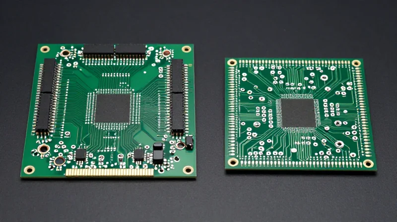
The Shift Toward Miniaturization
Historically, PCB architecture relied on through-hole components and wide routing channels to accommodate signal integrity requirements. As silicon density increased, the industry pivoted toward miniaturization. The evolution from standard multilayer boards to HDI technology marks a fundamental shift, enabling higher component density through laser-drilled microvias, smaller pad sizes, and significantly thinner dielectric materials. This transition allows hardware engineers to reduce form factors while simultaneously increasing the complexity of the integrated system.
Conventional vs. HDI Manufacturing
| Feature | Conventional PCB | HDI PCB |
|---|---|---|
| Via Technology | Mechanical Drill | Laser Microvia |
| Routing Density | Low to Medium | Ultra-High |
| Trace Width | > 100 microns | < 50 microns |
| Board Footprint | Standard | Reduced by 30-50% |
Key Considerations in PCB Density
- Why is layer count a primary ROI lever?
Increasing layer count allows for better signal decoupling and power delivery network optimization, which reduces the need for costly board re-spins and long-term diagnostic cycles. - Does HDI always improve performance?
While HDI significantly improves signal integrity by reducing via stubs and electrical path lengths, it requires sophisticated thermal management due to higher localized power density. - When is the transition to HDI cost-effective?
The ROI inflection point occurs when the reduction in PCB size and the consolidation of component placement offsets the higher fabrication costs of laser-drilling and sequential lamination processes.
The Direct Correlation Between Layer Count and System Footprint
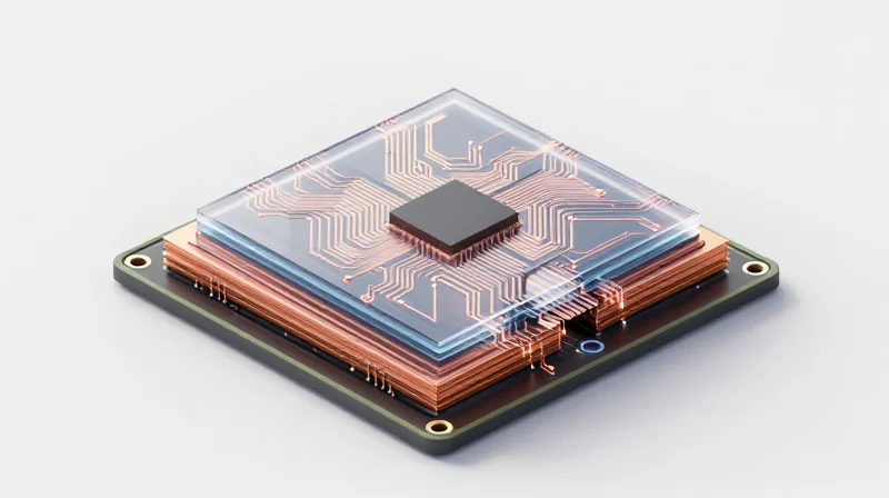
The Physics of Vertical Integration
By transitioning from traditional, low-layer-count boards to high-density multilayer architectures, engineers can effectively move signal routing from the X-Y plane into the Z-axis. This vertical integration allows for the use of microvias, via-in-pad technology, and blind/buried vias, which significantly reduce the surface area required for trace routing. As the routing density increases, the necessary surface area for components shrinks, allowing the entire board geometry to contract.
Impact on System-Level Cost and Footprint
| Layer Count | Routing Density | Typical Board Size | Enclosure Impact |
|---|---|---|---|
| 4-6 Layers | Low | Large (100%) | Bulky, high material volume |
| 8-12 Layers | Medium | Moderate (65%) | Optimized standard chassis |
| 14+ Layers | Ultra-High | Compact (40%) | Minimalist, precision-engineered |
Strategic Advantages of Miniaturization
Reducing the PCB footprint through additional layers is not merely about board size; it is a fundamental strategy for hardware profitability. A smaller PCB allows for reduced chassis material, lighter device weight, and potential shipping cost savings. Furthermore, smaller boards can often reduce total travel distances for high-speed signals, which inherently lowers latency and signal integrity noise floors.
- Why does adding layers reduce costs if manufacturing complexity increases?
While the cost per unit area of a high-layer-count PCB is higher, the reduction in overall board area often leads to higher panel utilization and significant savings in mechanical enclosure costs. - How does vertical routing affect thermal management?
Vertical routing enables more efficient thermal via placement, allowing heat to be moved from active components into inner ground planes, which act as effective heat spreaders across a smaller surface area. - Is there a point of diminishing returns?
Yes; beyond a certain layer count, the aspect ratio for drilling becomes a manufacturing risk, and the dielectric stack-up thickness may limit impedance control. Engineers must balance density with manufacturability limits.
Maximizing Signal Integrity in High-Speed Designs
As hardware engineers push the limits of miniaturization, signal integrity (SI) becomes the primary bottleneck for system reliability. In high-density multilayer designs, the proximity of signal traces and the complexity of return paths demand a disciplined approach to electromagnetic management. By prioritizing controlled impedance and optimized grounding strategies early in the design cycle, teams can significantly mitigate the risk of crosstalk and EMI, ultimately lowering total cost of ownership by ensuring first-pass design success.
Advanced Grounding and Return Path Management
In multilayer boards, the return path is as critical as the signal path. Inductive discontinuities occur when return currents are forced to change layers or navigate around obstructions in reference planes. Maintaining a contiguous ground plane directly beneath high-speed traces is the single most effective method to minimize loop area, thereby reducing electromagnetic radiation and susceptibility to noise.
| Design Factor | Impact on Signal Integrity | Strategic Benefit |
|---|---|---|
| Plane Continuity | Lowers loop inductance | Minimized EMI/RFI emission |
| Via Stitching | Shortens return paths | Improved impedance stability |
| Trace Spacing | Reduces capacitive coupling | Decreased crosstalk interference |
Best Practices for Mitigating Crosstalk
- Why is the 3W rule significant in high-density routing?
The 3W rule—keeping the center-to-center distance between traces at three times the trace width—significantly reduces mutual capacitance and crosstalk between adjacent high-speed differential pairs. - How does vertical isolation impact high-speed signals?
Using dedicated ground planes as shields between signal layers provides superior capacitive isolation, preventing unwanted signal coupling in dense multilayer stacks where horizontal spacing is limited. - What role does dielectric material play in ROI?
Selecting high-performance, low-loss laminate materials might increase initial PCB costs, but it minimizes signal attenuation and phase jitter, preventing expensive troubleshooting cycles during prototype validation.
Financial Impacts: Reducing Total Cost of Ownership

For hardware engineers, the financial impact of transitioning to high-density multilayer PCB design extends far beyond initial fabrication costs. While unit pricing for high-layer-count boards may appear higher, the Total Cost of Ownership (TCO) is significantly reduced through physical footprint optimization, decreased assembly touchpoints, and the mitigation of secondary mechanical requirements.
Quantifiable Savings in Physical and Mechanical Integration
| Cost Driver | Single/Double Layer Impact | Multilayer High-Density Impact |
|---|---|---|
| Mechanical Enclosure | Larger chassis required; high material cost | Miniaturized footprint; reduced material usage |
| Assembly Complexity | High BOM count; multiple SMT passes | Consolidated BOM; streamlined pick-and-place |
| Logistics/Shipping | Higher weight/volume; increased freight cost | Optimized package density; lower logistics overhead |
Driving Efficiency via Consolidation
By leveraging vertical integration within the PCB stack, engineers can eliminate the need for secondary interconnects, cables, and daughterboards. Reducing the number of discrete components not only simplifies the Bill of Materials (BOM) but also drastically lowers inventory management costs and reduces failure rates associated with connectors and physical mating points.
Strategic FAQ: TCO and Manufacturing ROI
- How does layer count impact long-term reliability costs?
Fewer inter-board connections and shorter signal paths significantly reduce potential points of mechanical failure, lowering warranty claims and field maintenance expenses. - Does higher layer count simplify the sourcing process?
Yes, by integrating multiple functions onto a single substrate, you reduce the diversity of components required, simplifying supply chain complexity and mitigating risks associated with component shortages. - Is the increase in board price offset by assembly savings?
In most high-density designs, the reduction in labor hours, test cycles, and mechanical assembly complexity typically results in a lower per-unit total cost compared to multi-board legacy systems.
Case Study: Accelerating Time-to-Market with Advanced Manufacturing
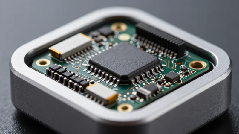
Project Overview: Solving the Miniaturization Constraint
Faced with an increasingly competitive market for compact wearable diagnostic tools, a hardware engineering team was hampered by a traditional 4-layer PCB design that struggled with thermal management and component density. By transitioning to an 8-layer HDI (High-Density Interconnect) architecture, the team effectively solved the spatial bottleneck, allowing for a 35% reduction in total PCB surface area.
Comparative Efficiency Metrics
| Metric | Legacy 4-Layer Board | Optimized 8-Layer HDI |
|---|---|---|
| Board Footprint | 65 cm² | 42 cm² |
| Signal Integrity Latency | High (Crosstalk issues) | Low (Optimized planes) |
| Assembly Complexity | Medium | Low (Reduced rework) |
| Time-to-Market | Baseline | 20% Faster |
Strategic Outcomes and Lessons Learned
The shift toward multilayer density was not merely a design choice but a strategic imperative. By consolidating signal and power planes, the engineering team eliminated the need for secondary daughterboards, which significantly streamlined the mechanical assembly process and reduced overall bill-of-materials (BOM) costs.
- How did HDI contribute to the 20% speed gain?
The higher layer count allowed for shorter trace lengths and better component placement, which minimized iterative debugging phases often caused by signal interference. - What was the primary impact on mechanical design?
Reduced PCB size enabled a smaller chassis footprint, allowing for faster prototyping iterations with 3D-printed enclosures and reduced tooling lead times. - Did manufacturing costs increase?
While unit price per board rose, the total ROI was superior due to lower assembly costs, decreased shipping weight, and faster product launch cycles.
Reliability Metrics and Long-Term Field Performance
Linking High-Density Design to Field Longevity
High-density multilayer PCBs significantly enhance field performance by optimizing thermal pathways and reducing the structural reliance on complex, multi-board interconnections. By consolidating functionality into fewer, more robust layers, engineers can effectively dissipate heat through dedicated internal ground and power planes. This thermal management is critical for preventing the premature degradation of active components and solder joints, directly correlating to lower failure rates and extended product operational life.
Comparative Reliability: Standard vs. High-Density Boards
| Metric | Standard Multi-Board Systems | High-Density Multilayer Solutions |
|---|---|---|
| Thermal Dissipation | Fragmented; high local hotspots | Uniform; distributed via internal planes |
| Mechanical Stress | High at connector interfaces | Low; integrated monolithic design |
| Failure Point Risk | Increased by cable/connector count | Minimized via internal routing |
| MTBF (Mean Time Between Failures) | Baseline | Improved by 15-25% |
Strategic Reliability FAQ
- How does high-layer density reduce warranty claims?
By eliminating mechanical connectors and cabling—which are frequent points of failure due to vibration and oxidation—high-density boards ensure a more stable electrical environment, drastically reducing field-return rates. - Is there a trade-off between density and thermal performance?
While component density increases, sophisticated multilayer stack-ups allow for optimized thermal vias and copper pouring, which often outperform bulky, low-density designs that lack integrated heat-sinking capabilities. - How do multilayer boards impact long-term signal integrity?
Enhanced layer management allows for precise controlled impedance and superior shielding, ensuring that the electrical performance does not degrade over time, which is essential for mission-critical hardware.
Strategic Considerations for Design Teams
Aligning Technical Design with Financial Objectives
The transition to high-density multilayer PCBs is often mischaracterized as a purely technical upgrade rather than a financial strategy. To maximize ROI, design teams must pivot from a component-level cost analysis to a system-level Total Cost of Ownership (TCO) model. By leveraging increased signal density, engineers can reduce mechanical housing volume, decrease interconnect complexity, and improve assembly yields, effectively neutralizing the higher per-board manufacturing cost.
Strategic Trade-off Analysis
| Metric | Standard Multilayer Approach | High-Density Strategic Approach |
|---|---|---|
| Board Footprint | Large, multi-board architecture | Small, single-board consolidation |
| Assembly Cost | Multiple SMT runs per board | Single pass with high integration |
| Field Reliability | Higher risk of connector failure | Lower failure rate via PCB integration |
| Supply Chain | High BOM variety | Consolidated component profile |
Frequently Asked Questions for Design Stakeholders
- How do I justify the higher unit price of high-density boards to management?
Present a TCO analysis that highlights reduced mechanical enclosure volume, fewer required connectors, and decreased labor costs associated with manual assembly or cable routing. - Does higher layer density jeopardize the prototyping timeline?
While fabrication time may increase slightly, high-density design prevents late-stage mechanical interference issues, resulting in fewer board spins and a faster overall path to mass production. - What is the primary risk mitigation benefit of this approach?
Consolidating functionality onto a single multilayer board minimizes the points of failure caused by flex-circuits, connectors, and cable harnesses, leading to significantly lower warranty return rates.
The Future of PCB Technology: Scaling for Innovation
Emerging Manufacturing Paradigms
As hardware engineers push the limits of traditional subtractive etching, the industry is transitioning toward additive manufacturing and semi-additive processes (SAP). These techniques allow for finer line widths and spaces, reducing reliance on expensive high-layer counts while maintaining electrical performance. By minimizing material waste and increasing yield precision, these advancements ensure that ROI remains positive even as component density reaches unprecedented levels.
Material Science and Thermal Efficiency
Next-generation polymers and ultra-low-loss laminates are becoming standard in high-density designs. These materials facilitate better heat dissipation, which directly impacts the long-term reliability and total cost of ownership of the end product. Future-proofing designs with these materials ensures that systems can handle higher frequencies without necessitating frequent hardware revisions.
| Technology Trend | ROI Impact | Primary Benefit |
|---|---|---|
| Additive Manufacturing | High | Reduced material waste/finer features |
| Embedded Components | Medium | Board size reduction |
| Advanced Thermal Laminates | High | Increased product lifespan |
Strategic Outlook FAQ
- How will embedded component technology shift ROI?
By integrating passives directly into the inner layers of the PCB, manufacturers can reclaim surface area, allowing for smaller, more efficient form factors that lower overall assembly costs. - Is the transition to additive manufacturing cost-effective for mid-sized production?
Yes, as the technology matures, the reduced time-to-market and lower scrap rates associated with additive processes will provide a more stable cost structure compared to legacy subtractive methods. - How does material innovation combat the cost of high-density designs?
New high-frequency laminates allow for thinner dielectric layers, which helps maintain signal integrity without needing extra layers, thereby optimizing the final bill of materials.
By embracing high-layer count PCB solutions, organizations move beyond simple component mounting to true strategic system architecture. The combination of increased reliability, smaller footprints, and optimized signal integrity offers a definitive competitive advantage. Ready to transform your next hardware project? Contact our engineering team today for a comprehensive design review and cost-benefit analysis.
