
In the race to market, every hour counts. Achieving a 24-hour assembly turnaround is not just about choosing the right manufacturer; it is about engineering a design that speaks the language of automated production. If your DFM strategy is flawed, you will face costly rework and shipping delays. This guide provides the technical blueprint to synchronize your design phase with manufacturing realities.
The Direct Correlation Between DFM and Assembly Speed

Eliminating Engineering Queries (EQs)
Engineering queries (EQs) are the primary bottleneck in fast-track assembly. When a design lacks DFM rigor—such as ambiguous solder mask clearances, non-standard component orientations, or inadequate thermal relief—the assembly house must halt production to seek clarification from the design team. By implementing strict DFM protocols during the design phase, you proactively resolve these ambiguities. A design that aligns perfectly with the CM's (Contract Manufacturer) capabilities allows production lines to proceed directly from programming to placement, bypassing the time-consuming 'stop-and-ask' cycle that typically adds days to lead times.
The Cost of Manual Intervention
Manual intervention in SMT is the enemy of throughput. Processes that require human touch, such as manual alignment of misaligned pads, hand-soldering of non-standard component footprints, or custom masking for wave soldering, disrupt the high-speed rhythm of automated pick-and-place machines. Proper DFM ensures the board layout is fully optimized for automated assembly, maximizing the efficiency of the line.
| Process Metric | Non-DFM Optimized Design | DFM Optimized Design |
|---|---|---|
| EQ Resolution Time | 24-72 Hours | 0 Hours |
| Setup Complexity | High (Manual Adjustments) | Low (Standardized Inputs) |
| Throughput Speed | Intermittent / Stalled | Maximum Rated Speed |
DFM Best Practices for Assembly Efficiency
- How does component orientation impact SMT speed?
Standardized orientation allows for faster programming of the pick-and-place nozzles and ensures consistent thermal profiles during reflow, preventing tombstoning. - Why is land pattern accuracy critical?
Precise footprints compatible with the CM's library eliminate solder bridging and misalignment, ensuring the automated optical inspection (AOI) system passes the board on the first attempt. - Can DFM eliminate the need for manual assembly?
Yes, by utilizing standard surface mount components and ensuring enough clearance for automated tools, manual soldering tasks are effectively eliminated.
Mastering Component Placement Rules

Strategic Component Placement for SMT Efficiency
Component placement is not merely a task of spatial efficiency but a precise engineering discipline that directly dictates the throughput of your SMT assembly line. By adhering to standardized clearance, orientation, and edge-proximity rules, you minimize the risk of mechanical collisions during nozzle traversal and prevent thermal shadowing that leads to uneven solder joint profiles.
Guidelines for Clearance and Uniformity
| Parameter | Recommended Practice | Rationale |
|---|---|---|
| Orientation | Uniform alignment | Reduces rotation logic for pick-and-place heads. |
| Edge Clearance | 3mm minimum from PCB edge | Prevents mechanical stress from panel de-paneling. |
| Component Pitch | Avoid fine-pitch near large parts | Reduces thermal differential and uneven heat distribution. |
Placement FAQ
- Why is uniform orientation so critical?
Uniform orientation reduces the number of nozzle rotation cycles during the pick-and-place process, significantly decreasing the total time per board and reducing mechanical wear on the assembly machinery. - What is the danger of placing heavy components too close to the board edge?
Components near the edge risk damage during the de-paneling process, as the mechanical stress exerted by the routing or scoring tool can cause solder joint fatigue or fractured components. - How does component density affect rework?
High-density placement with insufficient clearance prevents the application of rework tools, potentially turning a single faulty component into a total board loss if the surrounding components cannot be shielded during thermal application.
Standardizing Footprints for First-Pass Yield
The Critical Role of IPC-7351 Standardization
The foundation of a robust Design for Manufacturing (DFM) strategy lies in the strict adherence to the IPC-7351 standard for surface mount land patterns. When designers deviate from these specifications, they introduce variability that automated assembly equipment and reflow processes cannot compensate for. Standardizing footprints ensures that solder paste deposition and component-to-pad alignment remain consistent, directly reducing the probability of common assembly failures.
Impact of Non-Standard Footprints on SMT Defects
| Common Footprint Error | Resulting SMT Defect | Root Cause |
|---|---|---|
| Excessive Pad Length | Solder Bridging | Too much paste volume leading to bridging between adjacent pads. |
| Asymmetrical Pad Design | Tombstoning | Uneven wetting forces pulling the component off-pad during reflow. |
| Inadequate Thermal Relief | Cold Solder Joints | Excessive heat sinking prevents proper solder reflow at the joint. |
Addressing Design Variability FAQs
- Why should I avoid customizing land patterns for small passives?
Customization often inadvertently alters the solder paste stencil ratio, which disrupts the calculated wetting force balance required for high-speed pick-and-place, leading to increased tombstoning rates. - How does footprint standardization accelerate assembly cycles?
Standardized patterns allow for reliable, predictable solder paste deposits, eliminating the need for process engineers to perform iterative stencil modifications or manual touch-ups on the assembly line. - What is the most effective way to manage library footprints?
Implement a centralized, validated component library that mandates the use of IPC-compliant land patterns, preventing designers from creating ad-hoc footprints during the layout process.
By moving away from arbitrary land pattern creation and toward IPC-7351 compliance, design teams can ensure that their hardware is 'born' for manufacturability. This alignment not only streamlines the transition from prototype to production but also significantly lowers the cost of rework by catching potential solderability issues during the design phase rather than the reflow phase.
Optimizing Stencil Design for Precise Solder Deposition
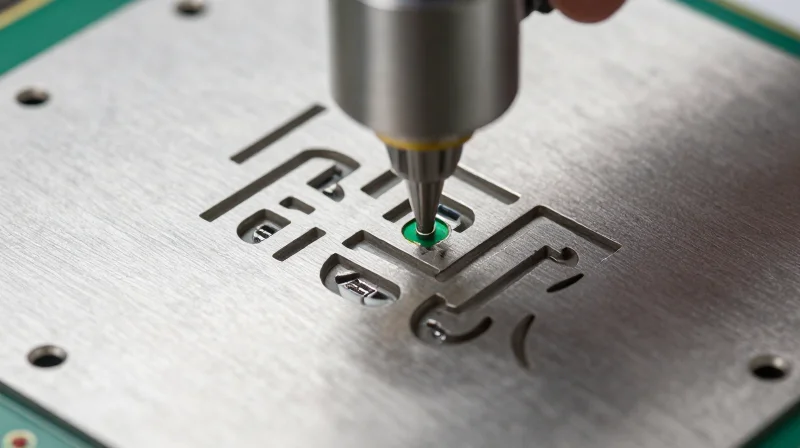
Stencil design is not merely a translation of copper footprints; it is a sophisticated engineering task that dictates the volume and shape of solder paste deposits. For high-density interconnections, poor aperture design is the primary cause of solder bridging and insufficient joint formation. Designers must balance paste release efficiency against the constraints of board topography to ensure that every pad receives the exact volumetric requirement for a reliable interconnect.
Strategic Aperture Scaling and Modification
Aperture scaling is essential to compensate for the relationship between the aperture wall area and the aperture volume (the area ratio). To achieve a standard 0.66 area ratio for reliable paste transfer, designers must employ specific geometric modifications for fine-pitch components.
| Feature | Strategy | Benefit |
|---|---|---|
| Fine-Pitch QFP/BGA | Aperture Shrink (5-10%) | Prevents bridging by reducing excess volume |
| Large Thermal Pads | Window-pane partitioning | Controls solder flow and prevents component tilt |
| Small Passive Components | Home-plate/Radius corners | Improves paste release from the stencil wall |
Selecting Stencil Thickness and Finish
The stencil thickness must be selected based on the smallest pitch component on the board. While a thinner stencil (e.g., 0.10mm) is ideal for 0201 or smaller passives, it may starve larger components. Use stepped stencils—where the thickness varies across the foil—if your design mixes ultra-fine pitch BGAs with large leaded components. Additionally, ensure the stencil material is laser-cut and electropolished to minimize friction between the paste and the stencil walls.
Stencil Design FAQs
- How does surface finish affect paste deposition?
Uneven surface finishes, such as HASL, create a non-planar foundation, which risks solder bridging. ENIG or Immersion Silver provide a flatter surface, allowing for more consistent stencil gasketing and precise paste deposits. - When is a stepped stencil necessary?
A stepped stencil is required when the volume requirements for components on the same board vary by more than 30%. It allows for thicker deposits on large pads while preventing excess paste on fine-pitch ICs. - What is the role of aperture rounding?
Rounding the corners of apertures reduces the surface area contact, significantly improving the paste release efficiency and ensuring that paste doesn't remain trapped in the corners of the stencil.
Preparing Files for Automated Optical Inspection (AOI)

Automated Optical Inspection (AOI) relies heavily on the integrity and accuracy of your CAD export data to establish a 'golden board' reference. When your Gerber and centroid files contain inconsistencies—such as mismatched designators, missing fiducials, or improper layering—AOI systems struggle to align the physical PCB with the theoretical model, leading to false negatives and increased inspection cycle times.
Essential Data Deliverables for AOI
| File Type | Key Requirement for AOI | Impact of Failure |
|---|---|---|
| Centroid (Pick & Place) | X/Y center coordinates and component rotation | Component misalignment/false shift errors |
| Gerber/ODB++ | Clearly defined copper patterns and solder mask apertures | Inaccurate component body vs. solder pad detection |
| NC Drill | Accurate hole locations and plating specs | Fiducial registration failure |
Best Practices for Registration and Fiducials
Fiducials act as the global registration markers for the AOI machine. Without them, the system cannot verify the PCB's physical position relative to the camera array. Ensure that fiducials are placed in an asymmetrical pattern to prevent board flipping errors and maintain a clear keep-out zone around each marker to prevent interference from silk-screen ink or copper traces.
Common AOI Preparation FAQs
- Does component rotation in the centroid file matter?
Yes. AOI systems compare the actual component orientation against your centroid file. Any discrepancy—even by a few degrees—will trigger a polarity failure, resulting in unnecessary flagging of correctly placed parts. - How many fiducials are required for effective AOI?
A minimum of three global fiducials is recommended for panel registration, with at least two placed at diagonally opposite corners to maximize the accuracy of the board coordinate system. - Should I include hidden or passive components in my AOI program?
Yes. Even small passives (0201 or 01005) must be included in your data output. Excluding them prevents the AOI from detecting tombstoning or improper alignment on those specific footprints.
/* Example check for proper centroid alignment */
Component_Ref: R1
Package: 0603
X_Center: 1250.50 mil
Y_Center: 450.25 mil
Rotation: 90.0 degrees
Layer: Top
Minimizing Complexity: Fiducials and Tooling Holes
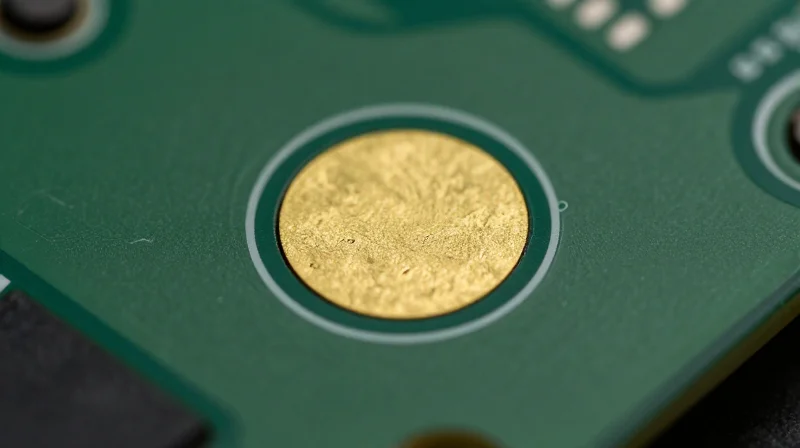
Accurate board registration acts as the heartbeat of the assembly line. Automated Placement Machines (pick-and-place) and Automated Optical Inspection (AOI) systems rely on fiducial marks to establish the global coordinate system of your PCB. If these marks are poorly designed, obscured, or misplaced, the machine vision system will fail to compensate for manufacturing tolerances, leading to placement offsets, short circuits, and mechanical misalignment.
Implementing Robust Fiducial Marks
To ensure reliable recognition, fiducials must provide high contrast against the board surface. The most effective approach is to utilize a bare copper pad with an opening in the solder mask, usually circular, ensuring it remains free of silkscreen or finish contaminants.
| Fiducial Characteristic | Recommended Design Parameter |
|---|---|
| Shape | Solid Copper Circle (1.0mm diameter) |
| Clearance | No solder mask/silkscreen in 2.0mm radius |
| Placement | Minimum 3 marks for global registration |
| Positioning | Not on the board edge; >5mm from frame |
Tooling Holes and Mechanical Alignment
While fiducials handle optical alignment, tooling holes provide the mechanical reference for board mounting and fixture handling. These holes should be non-plated to avoid copper burrs that could interfere with pin insertion or seating in the assembly jig.
- Why must fiducials be at least 5mm from the board edge?
This distance prevents damage during panelization or depaneling and ensures the machine's vacuum nozzle or conveyor rails do not interfere with the vision camera's line of sight. - Is a single fiducial sufficient?
No. A minimum of three global fiducials is required to calculate rotational offsets, X-Y shifts, and scaling distortions simultaneously. - Should I use local fiducials for fine-pitch components?
Yes. For BGA or QFN components with pitches below 0.5mm, local fiducials near the part footprint significantly improve placement precision by compensating for localized thermal expansion.
By standardizing these registration elements early in the design cycle, you eliminate ambiguity for the CM's setup engineers, directly translating into faster machine programming and reduced line-stop events during the manufacturing of your high-complexity assembly.
Common Technical Bottlenecks to Avoid
Even the most sophisticated PCB layouts can succumb to subtle technical oversights that trigger assembly line stoppages. By addressing these 'silent killers'—ranging from thermal connectivity issues to pad geometry irregularities—designers can drastically reduce rework and ensure a smoother path to final assembly.
Critical Design Bottlenecks
| Issue | Impact | Prevention Strategy |
|---|---|---|
| Inadequate Thermal Relief | Cold solder joints, difficult rework | Ensure web widths are 0.1mm minimum |
| Pad-to-Trace Asymmetry | Tombstoning, uneven heating | Maintain balanced trace widths on both sides |
| Solder Mask Encroachment | Short circuits, lack of wetting | Use 0.05mm mask relief beyond pad edge |
Frequently Encountered Assembly Barriers
- Why does thermal relief cause inconsistent solder joints?
If thermal relief spokes are too thin or improperly positioned, the copper plane acts as a massive heat sink, preventing the pad from reaching the liquidus temperature required for a robust intermetallic bond. - How do irregular pad-to-trace widths lead to tombstoning?
Connecting a wide trace to one side of a small chip component and a narrow trace to the other creates a thermal imbalance. During reflow, one side melts faster than the other, pulling the component upright due to unbalanced surface tension. - What is the consequence of missing solder mask dams?
Between fine-pitch pads, missing solder mask dams invite solder bridging during the wave or reflow process, which is nearly impossible to detect visually without high-resolution AOI, leading to potential field failures.
To further optimize, ensure your design rule check (DRC) includes strict constraints on silk-screen clearance. Components with markings covering pads are often flagged by automated systems as potential contaminants, leading to unnecessary manual inspections and shipment delays.
Collaborating with Your Manufacturer Early
Bridging the Gap Between Design and Fabrication
The most common cause of delayed assembly cycles is the discovery of non-manufacturable features after the order has been submitted. By initiating an early design review with your manufacturing partner, you leverage their specialized knowledge of line capacities, material constraints, and plating limitations. This collaborative approach transforms your DFM strategy from a reactive debugging process into a proactive optimization phase, ensuring your board is 'production-ready' before the first Gerber file is finalized.
Manufacturer-Led DFM vs. Internal Automated Checks
| Feature | Automated DFM Software | Manufacturer Design Review |
|---|---|---|
| Scope | Standard clearance checks | Process-specific capability constraints |
| Context | Design rule based | Factory floor equipment knowledge |
| Value Add | Fast error catching | Optimized yield and cost reduction |
Key Discussion Points for Assembly Alignment
- Material Selection
Confirm that your specified laminate and copper weights are currently in stock and optimized for your board's specific layer count and thermal requirements. - Panelization Strategy
Determine the optimal array size to maximize material utilization and compatibility with their pick-and-place equipment. - Component Sourcing
Verify that your selected footprint packages align with the manufacturer's preferred assembly profiles to avoid manual intervention. - Soldermask and Silkscreen
Define precise keep-out zones and resolution requirements to prevent manufacturing artifacts that could interfere with high-density assembly.
Ultimately, early engagement fosters a partnership where the manufacturer acts as an extension of your engineering team. By aligning your design files with their specific process windows, you mitigate the risk of 'on-hold' notifications, ensuring that your path to final assembly remains unobstructed and efficient.
By integrating these DFM principles into your workflow, you transform your design process from a reactive state to a proactive powerhouse, ensuring your products move from prototype to production in record time. Don't let avoidable design errors derail your timeline; download our DFM checklist or contact our engineering team for a pre-submission design audit to guarantee your next board passes inspection the first time.
