
Transitioning from a functional prototype to a mass-produced electronic product is where most hardware teams stumble. Hidden design errors often lead to expensive manual intervention or, worse, assembly line halts. This guide demystifies DFM, providing the industry-standard rules you need to ensure your PCB is 'factory-ready' from day one.
Understanding the DFM Advantage

The Strategic Value of DFM in Turnkey Assembly
DFM is not merely a set of restrictive rules; it is a strategic framework that aligns your design intent with the physical capabilities of fabrication and assembly equipment. By addressing potential manufacturing pitfalls early—such as trace clearance, component orientation, and thermal management—you eliminate the need for costly engineering changes (ECOs) once the design reaches the assembly floor. In a turnkey model, proactive DFM acts as a bridge between your engineering team and the contract manufacturer, ensuring that the transition from a digital design to a physical board is frictionless.
DFM Impact: Traditional vs. Optimized Design Workflows
| Attribute | Traditional Design | DFM-Optimized Design |
|---|---|---|
| Tooling Delays | Frequent | Minimal |
| Assembly Yield | Variable/Low | High/Predictable |
| Time-to-Market | Extended by Revisions | Accelerated |
| Unit Cost | Higher (hidden rework) | Lower (optimized processes) |
Common DFM Implementation FAQs
- Does DFM limit creative design?
No, DFM provides the boundaries within which innovation occurs. By understanding manufacturer tolerances, you can design complex boards that are actually manufacturable rather than technically brilliant but impossible to assemble. - Why does DFM lower total cost of ownership?
The highest costs in PCB production occur during rework and yield loss. DFM minimizes these events, drastically reducing the labor-intensive troubleshooting and component scrap rates that drive up long-term costs. - When should DFM analysis begin?
DFM must be integrated during the schematic and layout phase. Waiting until the board is ready for the assembly house often results in expensive re-spins that negate the speed advantages of turnkey assembly.
Standardizing Component Selection
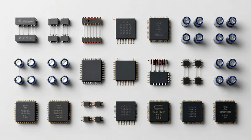
The Strategic Value of Component Standardization
Standardizing your Bill of Materials (BOM) is not merely a cost-saving measure; it is a critical risk mitigation strategy for turnkey assembly. By favoring parts currently in high volume or held in stock by assembly partners, designers effectively bypass long lead times and prevent the 'custom-part trap' where obscure components stall production for weeks. Selecting industry-standard packages reduces the overhead for pick-and-place machines and ensures your design remains resilient against localized supply shortages.
Preferred Parts vs. Custom Selection
| Feature | Preferred/Standard Parts | Custom/Obscure Parts |
|---|---|---|
| Sourcing Availability | High (Multi-vendor) | Low (Single-source/EOL risk) |
| Lead Times | Short/Stable | Extended/Unpredictable |
| Assembly Cost | Lower (Batch efficiency) | Higher (Manual/Setup fees) |
| BOM Resilience | High | Low |
Best Practices for BOM Management
- How do I define a 'Preferred Part'?
A preferred part is one that your assembly partner already stocks or uses frequently in their current production volume, ensuring they have established supply chains and validated machine profiles. - Why should I avoid unique packages?
Uncommon packages or non-standard form factors increase setup time and may require specialized nozzles or feeder configurations on assembly equipment, leading to higher NRE charges. - What is the role of cross-referencing?
Always specify at least two alternative manufacturers for critical components. If the primary choice becomes unavailable, an approved alternative ensures production continues without needing a new board spin or design review.
Ultimately, the goal is to align your design intent with the reality of the manufacturer's inventory. Before finalizing your schematic, consult your assembler's 'Preferred Parts List' (PPL). Aligning your design with their existing capabilities reduces the need for secondary sourcing efforts and ensures a seamless transition from prototype to full-scale manufacturing.
Optimizing Pad Patterns and Solder Mask Clearance
The Importance of IPC-Compliant Footprints
Standardized footprint design is the foundation of high-yield assembly. By adhering to IPC-7351 guidelines, designers ensure that pads provide enough surface area for fillets while minimizing the risk of solder bridges and tombstoning. Deviating from these standards often leads to poor wetting or mechanical instability during the reflow process.
Solder Mask Defined Clearance (SMD) vs. Non-Solder Mask Defined (NSMD)
| Feature | NSMD (Recommended) | SMD |
|---|---|---|
| Copper Definition | Copper is smaller than solder mask opening | Solder mask overlaps copper pad |
| Reliability | Superior for BGA/fine pitch | Better for rugged environments |
| Solder Joint | Solder grips sides of copper | Solder sits strictly on top |
For fine-pitch components like BGAs and QFNs, NSMD (Non-Solder Mask Defined) is the industry standard. This allows for better solder joint elasticity and significantly improves thermal fatigue resistance.
Common Assembly Pitfalls
- What happens if my solder mask clearance is too small?
Small clearances often lead to 'solder mask encroachment,' where the mask overlaps the copper pad, leading to uneven solder distribution and potential open circuits. - Why should I avoid placing vias in pads (VIPPO) without plugging?
Unplugged vias in pads cause 'solder wicking,' where solder travels down the hole during reflow, starving the joint and creating unreliable electrical connections. - How does asymmetric pad design affect production?
Asymmetry creates unequal thermal mass, which is a leading cause of tombstoning, especially for small passive components like 0201 or 0402 capacitors.
Effective PCB Panelization Strategies
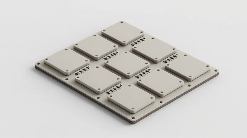
Panelization transforms individual circuit boards into a larger array, which is critical for automated surface-mount technology (SMT) lines to process boards efficiently. A well-engineered panel strategy reduces material waste, minimizes mechanical stress on components during the singulation process, and ensures stable handling through pick-and-place machinery.
Selecting the Right Panelization Method
| Method | Best Use Case | Key Advantage |
|---|---|---|
| V-Score | Rectangular boards with edge-to-edge layout | High density; no wasted space between boards. |
| Tab-Routing | Odd-shaped boards or overhanging components | Superior support for complex geometries. |
| Punch/Perforation | High-volume, thin PCB material | Fast separation for low-cost, high-speed lines. |
Essential Rules for Panel Design
- Maintain Minimum Edge Margins
Ensure at least 3-5mm of rails on the parallel sides of the panel to provide enough grip for conveyor systems and prevent board warping. - Strategic Fiduciary Placement
Place at least three fiducial marks on the rails at opposite corners to allow the vision system of pick-and-place equipment to orient the panel accurately. - Component Clearance
Avoid placing sensitive SMD components or connectors within 1mm of the board edge where singulation stress may cause solder joint fractures. - Symmetry and Balance
Maintain a symmetric distribution of boards across the panel to ensure uniform thermal distribution during reflow and consistent mechanical load during handling.
FAQs on Panelization Efficiency
- Why is board rotation important in panel design?
Rotating individual units by 180 degrees can often nest odd-shaped boards together, significantly reducing the amount of raw laminate discarded as scrap. - How do I know which break-out tab width to use?
Use at least three tabs for larger boards to maintain structural integrity during assembly, but keep them narrow enough to minimize the labor required for de-paneling.
Best Practices for Component Placement
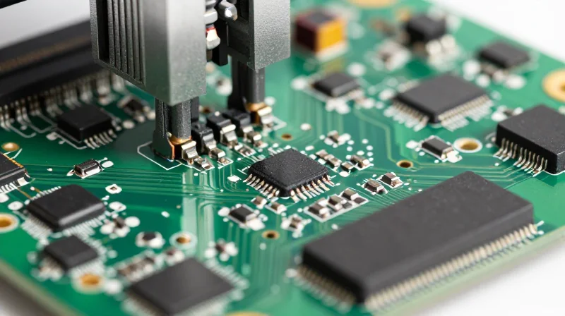
Strategic Orientation for Automated Assembly
To optimize the efficiency of pick-and-place (P&P) machines, components should ideally be oriented in a uniform direction. This minimizes the rotation cycles the machine must perform during assembly, significantly reducing the total placement time per board. Aligning all passive components in the same orientation allows the nozzle to maintain consistent pick-and-place kinematics, which increases machine uptime and reduces wear on rotation motors.
Critical Spacing and Clearance Rules
Adhering to strict clearance rules is not only about preventing electrical shorts; it is essential for the maneuverability of the assembly head. If components are placed too close to the board edge or adjacent tall parts, the machine may experience collisions or require slower placement speeds to maintain precision.
| Parameter | Minimum Clearance (Standard) | Why it matters |
|---|---|---|
| Board Edge | 5mm | Prevents rail interference and protects components during handling. |
| Component to Component | 0.5mm | Ensures adequate room for rework and prevents solder bridges. |
| Solder Mask Clearance | 0.1mm | Required to account for pick-and-place registration tolerances. |
Common Placement Pitfalls (FAQ)
- How do tall components affect placement?
Tall components can shadow smaller parts and impede the nozzle path. Keep connectors and large electrolytics away from fine-pitch ICs to ensure the head can access all pads without risk of collision. - Does component orientation matter for reflow?
Yes. If components are placed in a way that creates thermal imbalances—such as large ground planes adjacent to tiny passives—the risk of tombstoning increases significantly during the reflow process. - Are there specific rules for heavy components?
Heavy components should be placed near the edges of the board that correspond to the conveyor rails to reduce board flexing during the placement process, which helps maintain high-accuracy placement.
Silkscreen and Fiducial Mark Integrity
Silkscreen and fiducial marks represent the communication bridge between your CAD design and the factory floor. While silkscreen provides human-readable assembly guidance, fiducial marks are the essential geometric references that allow Pick and Place (P&P) machines and Automated Optical Inspection (AOI) systems to calibrate their coordinate systems, ensuring components land precisely on their intended pads.
The Anatomy of Reliable Fiducials
Fiducials are not merely arbitrary shapes; they are high-contrast alignment markers required for machine vision. Improperly designed fiducials can lead to assembly line stoppages or significant yield loss due to cumulative placement errors.
| Feature | Requirement for Assembly | Reason |
|---|---|---|
| Shape | Solid Circle | Best contrast and symmetry for optical sensors. |
| Diameter | 1.0mm to 3.0mm | Standard size for machine vision capture ranges. |
| Soldermask | Keep-out area required | Prevents optical interference from copper contrast. |
| Placement | Min 3 markers per board | Allows for accurate global translation and rotation mapping. |
Silkscreen Design Best Practices
Effective silkscreening reduces the risk of technician error during manual assembly or rework. However, poor design can introduce manufacturing defects if ink overlaps onto pads or interferes with solder wetting.
- Clearance Rules
Maintain a minimum of 0.15mm to 0.25mm of clearance between silkscreen markings and any exposed copper or solder mask openings to ensure high-quality prints without contamination. - Legibility Standards
Use a minimum stroke width of 0.125mm and a height of at least 1.0mm to ensure text remains crisp and readable after standard assembly processes. - Orientation Consistency
Standardize the rotation of component designators and polarity indicators to facilitate quick scanning by assembly operators.
Common Pitfalls in Mark Integrity
- Why do machines reject my panels?
Often caused by lack of global fiducials on the panel frame or insufficient contrast between the fiducial and the surrounding soldermask or substrate. - Can I put text over pads?
No; printing over pads causes uneven solder paste deposition, leading to tombstoning or poor joint integrity. Always clip silkscreen elements that intersect with pads. - Do I need fiducials for single boards?
Yes. Even if your design is simple, most modern assembly houses require fiducials for accurate laser or camera-assisted alignment during the mounting process.
Thermal Management and PCB Stackup

Thermal Management Strategies
Heat dissipation is not merely a post-assembly concern; it starts with layout. Poor thermal distribution creates localized stress points that lead to board warping during reflow, impacting solder joint integrity. Engineers must utilize internal copper planes as heat sinks and prioritize proper thermal relief patterns for high-power components to ensure uniform heat distribution.
PCB Stackup Design for Structural Stability
A balanced copper stackup is essential to minimize thermomechanical stress. If copper distribution is significantly uneven between the top and bottom layers, the board will bow during the rapid heating phases of reflow. Aim for symmetrical construction by mirroring copper weight and density across the neutral axis of the board.
| Design Element | Thermal Impact | Assembly Consideration |
|---|---|---|
| Copper Pour Density | Distributes heat uniformly | Reduces board warping/bowing |
| Thermal Vias | Lowers junction temperature | Requires tenting or plugging |
| Stackup Symmetry | Prevents mechanical stress | Crucial for thin/flexible boards |
Common Thermal Design FAQs
- Why does asymmetric copper cause warping?
Asymmetric copper expansion rates under heat create a mechanical bending moment, leading to board deformation during the reflow process. - How do thermal reliefs improve yield?
Thermal reliefs restrict heat transfer from the pad to the ground plane, ensuring the solder joint reaches proper reflow temperature without requiring excessive iron or oven heat. - Are thermal vias necessary for all components?
No, they are primarily reserved for components with high TDP (Thermal Design Power). Excessive use can complicate the manufacturing process and increase cost.
Pre-Production Design Reviews
Automated DFM vs. Manual Peer Review
A robust pre-production strategy requires a layered approach. While automated software excels at catching geometric rule violations, manual peer reviews are essential for identifying functional intent gaps and manufacturability nuances that algorithms often overlook.
| Feature | Automated DFM Analysis | Manual Peer Review |
|---|---|---|
| Primary Goal | Geometric validation | Design intent verification |
| Error Detection | Clearance, trace width, silkscreen | Logical flaws, component sourcing issues |
| Consistency | Perfect | Variable based on expertise |
Critical DFM Checkpoints
To ensure your design is ready for a turnkey assembly line, your review process must focus on the convergence of digital data and physical manufacturing constraints.
- Why is automated DFM analysis insufficient on its own?
Automated tools check against a database of static rules, but they cannot assess if your component selection is prone to obsolescence or if your thermal dissipation strategy is adequate for your specific application. - How should you approach a design review?
Start with a software-based DRC (Design Rule Check) to resolve physical conflicts, followed by a cross-functional review involving layout engineers and assembly technicians to identify potential assembly bottlenecks. - What role do assembly houses play in the review process?
Many reputable assembly partners offer a DFM audit as part of their quoting process; leverage this by requesting feedback on your fiducial placement, panelization, and solder mask expansion before moving to production.
Final Validation Checklist
Before pushing to production, verify the following: ensure all bill of materials (BOM) items are currently in stock, confirm that drill files match the stackup specifications exactly, and run a final 3D clearance simulation to identify hidden mechanical collisions that 2D views might conceal.
By integrating these DFM principles into your design workflow, you move beyond mere functionality and create a scalable product ready for the rigors of mass production. Do not let design oversights compromise your project timeline. Contact our engineering team today for a comprehensive DFM audit of your next board design.
