Ceramic PCB: The Ultimate Guide to Material, Benefits, and Applications
In the rapidly evolving landscape of electronics, the demand for materials that can withstand extreme conditions is ever-increasing. Enter ceramic PCBs, a technology that leverages the unique properties of ceramics to deliver exceptional performance. From the depths of space to the core of high-performance computing, ceramic PCBs are silently revolutionizing how electronics are designed and used. This article delves into the core aspects of ceramic PCBs, illuminating their advantages, drawbacks, and diverse applications. We’ll explore how these tiny technological marvels are shaping the future of electronic innovation.
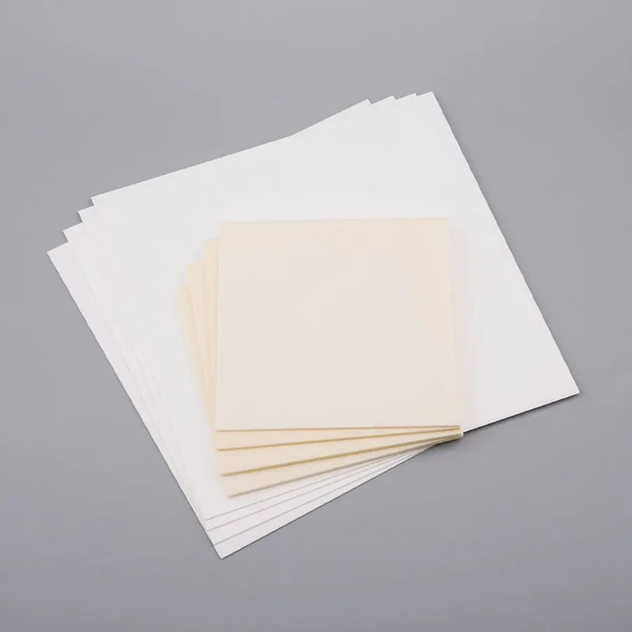
What is a Ceramic PCB?
A ceramic PCB is a type of circuit board that utilizes ceramic materials as its base substrate, providing enhanced performance characteristics compared to traditional FR4 (Flame Retardant 4) boards. These characteristics include superior thermal conductivity, exceptional electrical insulation, and remarkable resistance to harsh environmental conditions, making them ideal for demanding applications.
Unlike conventional PCBs that are based on materials like fiberglass-reinforced epoxy resins, ceramic PCBs leverage the inherent properties of ceramic compounds. These properties result in circuit boards that are significantly more robust and reliable in high-stress environments where heat dissipation, electrical isolation, and durability are critical factors. The choice of ceramic material dictates the specific performance parameters, allowing for a tailored approach to meet diverse application needs.
Key Materials in Ceramic PCB Fabrication
The performance and application suitability of a ceramic PCB are fundamentally determined by the ceramic materials used in its construction. These materials, selected for their unique properties, offer a range of characteristics from thermal conductivity to electrical insulation, and are crucial to enabling the high-performance capabilities of ceramic PCBs. The primary materials utilized are alumina (Al2O3), aluminum nitride (AlN), zirconia (ZrO2), and beryllium oxide (BeO), each offering distinct advantages for specific applications.
| Material | Chemical Formula | Thermal Conductivity (W/m·K) | Dielectric Constant | Key Applications | Advantages | Disadvantages |
|---|---|---|---|---|---|---|
| Alumina | Al2O3 | 20-35 | 9-10 | General purpose, hybrid circuits, power electronics | Cost-effective, high mechanical strength, good electrical insulation | Lower thermal conductivity compared to AlN |
| Aluminum Nitride | AlN | 140-180 | 8-9 | High power modules, LED lighting, RF applications | Excellent thermal conductivity, high electrical insulation | Higher cost, more challenging to manufacture |
| Zirconia | ZrO2 | 2-3 | 20-30 | High temperature sensors, medical implants, fuel cells | High mechanical strength, high temperature resistance, chemical inertness | Low thermal conductivity, higher cost |
| Beryllium Oxide | BeO | 250-300 | 6-7 | High-power RF and microwave devices, aerospace applications | Exceptional thermal conductivity, low dielectric constant | High toxicity, environmental and safety concerns |
The choice of material depends on the specific performance requirements of the application. Alumina is a cost-effective solution where extremely high thermal performance is not required. AlN is preferred when managing high heat is critical. Zirconia, though less thermally conductive, excels in high-temperature and harsh chemical environments. BeO, while offering superior thermal properties, is constrained by its toxicity and safety concerns, thereby limiting its applications to highly specialized fields where performance is paramount and safety measures are stringent. Understanding these trade-offs is essential in the design of ceramic PCBs.
Advantages of Ceramic PCBs
Ceramic PCBs offer a suite of performance advantages over traditional FR-4 boards, primarily stemming from the inherent properties of ceramic materials. These benefits make them ideal for demanding applications requiring high reliability and performance in harsh conditions. The primary advantages include superior thermal management, high temperature resistance, excellent electrical insulation, high mechanical strength, and exceptional chemical stability.
Disadvantages and Challenges of Ceramic PCBs
While ceramic PCBs offer many advantages, they also present certain disadvantages and challenges that must be considered. These primarily revolve around higher costs, manufacturing complexities, and material limitations, which, although being actively addressed, still pose considerable engineering hurdles.
- Higher Cost
Ceramic materials and the specialized processing methods involved in their fabrication contribute to a higher production cost compared to FR-4 PCBs. This cost increase is due to both the raw materials and more complex manufacturing processes. - Manufacturing Complexity
Ceramic PCBs require precise control and specialized equipment for fabrication. The processes such as sintering, metallization, and via formation necessitate advanced techniques and skilled personnel, leading to increased manufacturing difficulty. - Potential Brittleness
Ceramic materials, while possessing high mechanical strength, can be brittle and susceptible to cracking under mechanical stress or impact. This brittleness needs careful consideration during handling and application, impacting design and reliability. - Limited Substrate Size
Due to manufacturing constraints and material properties, large-size ceramic PCBs can be difficult and expensive to produce, which limits the size of circuits that can be produced compared to FR-4 PCBs. - Difficult Rework and Repair
Repairing or reworking ceramic PCBs is more difficult than standard PCBs due to the delicate nature of the material and the precision required in the manufacturing process. This factor increases the expense of repair.
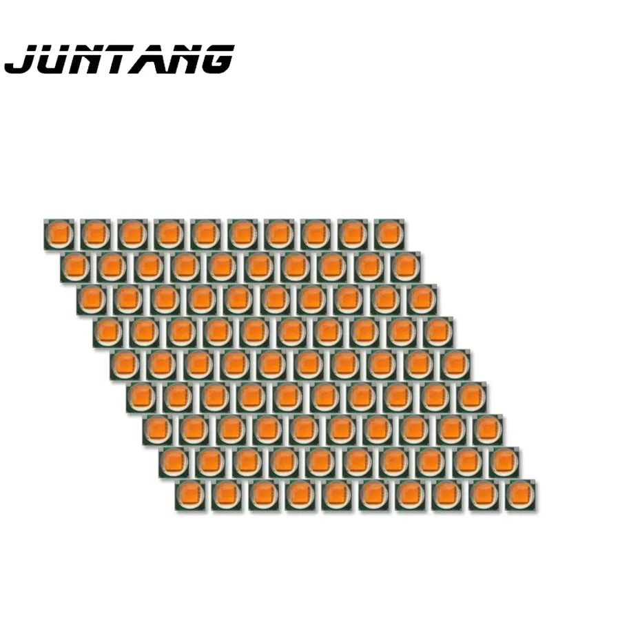
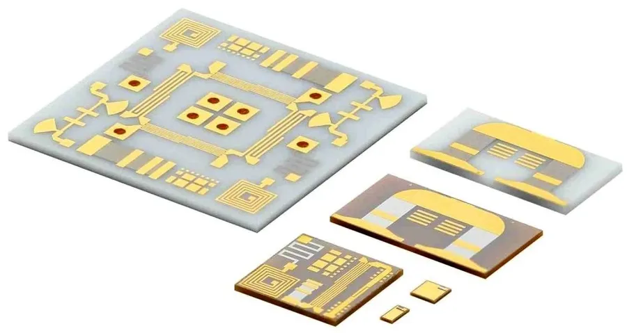
Types of Ceramic PCBs
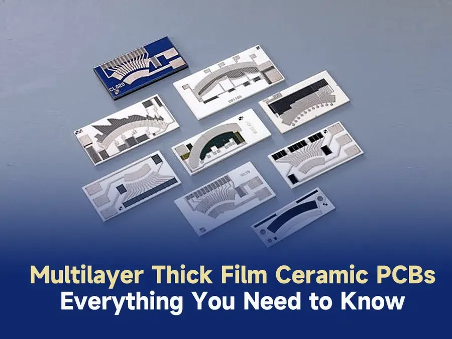
Ceramic PCBs are not monolithic in their construction; rather, they are fabricated using different processes resulting in distinct types, each tailored for specific applications. These include thick film, thin film, and Low-Temperature Co-fired Ceramic (LTCC) PCBs, each with unique characteristics in terms of fabrication, performance, and cost.
| Type | Process | Key Features | Typical Applications |
|---|---|---|---|
| Thick Film | Screen printing of conductive pastes onto ceramic substrates | Cost-effective for large-scale production, Larger feature sizes, Suitable for high-power applications | Power electronics, Heaters, Sensors |
| Thin Film | Deposition and etching of thin layers of metal on ceramic substrates | High precision, Fine line and space, excellent electrical performance | High frequency applications, Microelectronics, RF devices |
| LTCC (Low Temperature Co-fired Ceramic) | Lamination of multiple layers of ceramic tape with embedded conductors, fired at relatively low temperatures | Integration of complex 3D structures, High density interconnect, Excellent reliability | Aerospace, Automotive, High-frequency communication systems |
The choice between thick film, thin film, and LTCC technologies depends on the specific application requirements, including cost considerations, the precision needed for conductive features, and the complexity of the circuit design. Each type offers unique advantages and limitations, which engineers carefully weigh when designing electronic systems with ceramic PCBs.
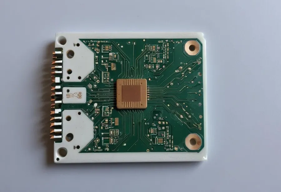
Applications of Ceramic PCBs
Ceramic PCBs, owing to their superior thermal, electrical, and mechanical properties, are indispensable in high-performance applications across diverse industries. Their ability to withstand extreme temperatures and harsh environments makes them suitable for scenarios where traditional FR-4 PCBs would fail.
- Aerospace
In aerospace, ceramic PCBs are used in critical systems such as radar, satellite communication, and avionics. Their ability to function reliably under extreme temperature variations and vibration is crucial for the performance and safety of these systems. For example, they are found in the control systems of aircraft engines and in high-frequency communication modules used in satellite systems. - Automotive
The automotive industry is increasingly adopting ceramic PCBs for applications in engine control units (ECUs), LED lighting systems, and advanced driver-assistance systems (ADAS). Their high-temperature resistance is particularly beneficial for ECUs located near the engine. They also provide improved reliability in harsh automotive environments where vibration, moisture, and temperature fluctuations are common. They are found in advanced lighting systems and in the complex control systems of electric vehicles. - High-Power Electronics
Ceramic PCBs are essential in high-power electronics applications such as power converters, inverters, and solid-state relays. Their superior thermal conductivity enables efficient heat dissipation, preventing thermal runaway and ensuring reliable performance of high-power devices. This is particularly important in applications like renewable energy systems (solar and wind) and industrial power supplies. Specific examples include motor controllers for industrial automation and power transmission systems for high voltage grids. - Medical Devices
In medical devices, ceramic PCBs are utilized in diagnostic equipment such as MRI machines, X-ray equipment, and implantable devices. Their biocompatibility and ability to withstand sterilization processes make them ideal for these applications. The high precision and reliability they offer are essential for patient safety. Examples include precision sensors and control electronics for implantable pacemakers and imaging systems for diagnostic purposes. - LED Lighting
Ceramic PCBs are increasingly used in high-power LED lighting applications due to their excellent thermal management capabilities. Their ability to dissipate heat efficiently ensures consistent performance and longevity of LED lighting modules. These are found in high-brightness applications like automotive headlamps, industrial lighting, and large-scale commercial LED displays. Their use also enables smaller, more efficient lighting designs.
Ceramic PCB vs. FR-4 PCB: A Detailed Comparison
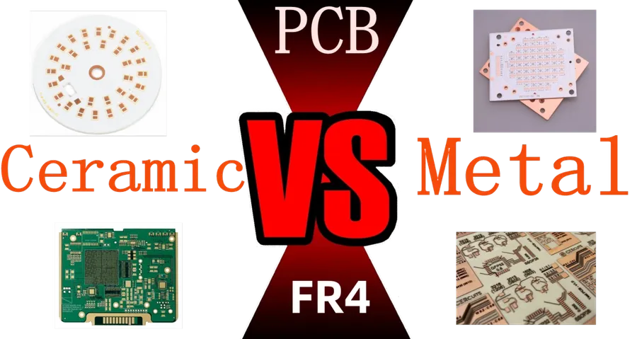
Ceramic PCBs and FR-4 PCBs represent two distinct approaches in circuit board manufacturing, each with unique performance characteristics and application suitability. Understanding their differences is crucial for selecting the appropriate material for a given application. Ceramic PCBs offer superior thermal and electrical properties at a higher cost, while FR-4 PCBs are a cost-effective and versatile standard.
| Characteristic | Ceramic PCB | FR-4 PCB |
|---|---|---|
| Thermal Conductivity | High (15-300 W/m·K, depending on material) | Low (0.2-0.4 W/m·K) |
| Operating Temperature | Very High (up to 350°C and higher, material dependent) | Moderate (up to 130°C) |
| Electrical Insulation | Excellent | Good |
| Mechanical Strength | High | Moderate |
| Chemical Resistance | Excellent | Good |
| Cost | High | Low |
| Manufacturing Complexity | High | Low |
| Application Suitability | High-power electronics, high-temperature applications, aerospace, medical, automotive | General-purpose electronics, consumer devices, low-cost applications |
| Dimensional Stability | Excellent | Moderate |
| Moisture Absorption | Very Low | Moderate |
Frequently Asked Questions About Ceramic PCBs
This section addresses common inquiries regarding ceramic PCBs, covering aspects from their performance characteristics to design considerations and applications. We aim to provide concise, authoritative answers to help you better understand these specialized circuit boards.
- What is the maximum operating temperature for a ceramic PCB?
Ceramic PCBs can typically operate at significantly higher temperatures than FR-4 PCBs. Depending on the specific ceramic material, they can withstand temperatures ranging from 150°C to over 350°C. For instance, aluminum nitride (AlN) PCBs can operate at the higher end of this range, while alumina (Al2O3) PCBs have slightly lower limits. The exact maximum temperature depends on the materials and manufacturing process used. - What are the different types of ceramic PCBs?
Ceramic PCBs are categorized mainly by their fabrication process. The primary types include thick film, thin film, and Low Temperature Co-fired Ceramic (LTCC) PCBs. Thick film PCBs involve screen-printing conductive and dielectric pastes onto the ceramic substrate. Thin film PCBs employ deposition and etching techniques to create fine features. LTCC PCBs utilize a multi-layer ceramic structure with co-fired layers, enabling more complex designs. - Are ceramic PCBs more expensive than FR-4 PCBs?
Yes, ceramic PCBs are generally more expensive than FR-4 PCBs. This is mainly due to the higher cost of ceramic materials, more complex manufacturing processes, and specialized equipment required. The increased material cost, especially for high-purity ceramics like aluminum nitride, contributes significantly to the overall cost. The specific cost depends on the type of ceramic, the design complexity, and the production volume. - What are the primary advantages of using a ceramic PCB?
Ceramic PCBs offer several advantages, including superior thermal conductivity, excellent electrical insulation, high-temperature resistance, high mechanical strength, and chemical stability. These properties make them suitable for high-power electronics, aerospace, automotive, and other applications where extreme conditions and high reliability are critical. Their ability to dissipate heat efficiently is a major advantage in high-power applications. - What are some common applications of ceramic PCBs?
Ceramic PCBs find use in a variety of applications such as aerospace electronics (e.g., satellite systems), high-power LEDs, automotive sensors and control systems, medical implants and diagnostics, and industrial power modules. Their high thermal conductivity and durability make them suitable for these environments, where reliability and performance are essential. - Are there any limitations to using ceramic PCBs?
Yes, some limitations include the higher cost compared to FR-4, manufacturing complexity (particularly for multi-layer designs), and potential brittleness, especially with some ceramic types. They also have a more limited choice of materials and a less flexible process than FR-4 PCBs. Addressing these limitations often requires advanced fabrication techniques and careful material selection. - Can ceramic PCBs be used in high-frequency applications?
Yes, ceramic PCBs are well-suited for high-frequency applications due to their low dielectric loss and stable electrical properties. Materials like alumina and aluminum nitride offer consistent performance at microwave and millimeter-wave frequencies. This makes them suitable for RF and microwave applications where signal integrity and minimal losses are crucial.
Future Trends in Ceramic PCB Technology
The field of ceramic PCB technology is rapidly evolving, driven by the increasing demands for high-performance electronics in extreme environments. Current research focuses on developing novel materials, refining fabrication techniques, and exploring new applications. These advancements aim to overcome existing limitations, such as cost and brittleness, while enhancing the performance and versatility of ceramic PCBs.
- Advanced Material Research
Ongoing investigations into new ceramic compositions, such as modified aluminum nitride (AlN) and silicon carbide (SiC), to enhance thermal conductivity, mechanical strength, and electrical insulation properties. Nanomaterials are also being explored to improve material characteristics at a micro level. - Improved Fabrication Techniques
Advancements in manufacturing processes, including additive manufacturing (3D printing) and laser direct structuring, to reduce production time, lower costs, and allow for more complex and customized designs. These methods also aim to reduce material waste and improve precision. - Integration with Advanced Packaging
The integration of ceramic PCBs with advanced packaging technologies, such as System-in-Package (SiP) and 2.5D/3D packaging, is driving the development of smaller, more efficient, and more functional electronic modules. This is particularly relevant for applications in high-frequency and high-density electronics. - Application in Emerging Sectors
Exploration of new application areas in emerging sectors, including electric vehicles (EVs), 5G and 6G communication infrastructure, high-performance computing, and advanced medical devices. Ceramic PCBs are increasingly becoming a critical component in these cutting-edge technologies, where reliability and performance are paramount. - Sustainability Initiatives
Efforts to develop more sustainable fabrication methods and materials, including the reduction of energy consumption, the minimization of waste, and the exploration of bio-based ceramic materials. These initiatives address the growing need for environmentally friendly electronics manufacturing processes.
Ceramic PCBs are not just an alternative; they represent a significant leap forward in PCB technology. Their unmatched thermal management capabilities, coupled with superior electrical and mechanical properties, position them as indispensable in high-performance and harsh environment applications. As technology advances, innovations in ceramic PCB design and fabrication will pave the way for even more sophisticated devices, pushing the limits of what's possible in electronics and solidifying the crucial role of ceramic PCBs in future developments.