Choosing the Right PCB Factory: A Comprehensive Guide
In our increasingly interconnected world, printed circuit boards (PCBs) are the unsung heroes powering countless devices, from smartphones to industrial machinery. Selecting the right PCB factory is crucial for ensuring the success of any electronics project. This article will help you navigate the complexities of PCB manufacturing, providing actionable advice to help you find a partner who can deliver high-quality PCBs that meet your specific requirements, thus helping you to understand the production process of [pcb factory] and make more professional and wise decisions.
Understanding PCB Manufacturing Processes
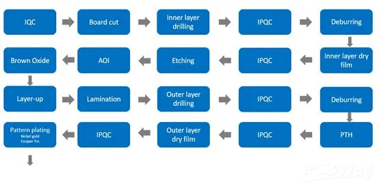
The printed circuit board (PCB) manufacturing process is a complex multi-stage undertaking, transforming a digital design into a physical, functional electronic component. This section details the fundamental steps involved in creating a PCB, highlighting the diverse technologies and considerations employed by a PCB factory to produce boards of varying complexities and specifications.
- PCB Design & Layout
This initial phase converts electronic schematics into a physical layout using specialized software (CAD). This includes component placement, trace routing, and defining board layers. - Film Generation
The layout data is transferred to photoplots, creating photographic films representing the layers of the PCB. These films will be used in the imaging process. - Inner Layer Imaging
Photoresist, a light-sensitive material, is applied to copper-clad laminates and exposed to UV light through the photoplots. This process creates the patterns for each layer on the copper. - Etching
The exposed photoresist is hardened, and the unwanted copper is removed using chemical etchants, leaving behind the desired circuit traces. This step defines the conductive pathways of the PCB. - Layer Alignment and Lamination
Multiple etched layers are carefully aligned and laminated together using heat and pressure, forming a multilayer PCB structure. - Drilling
Holes are drilled through the laminated PCB to accommodate component leads and vias (conductive pathways between layers). These holes often require precise positioning and size. - Plating
The drilled holes are plated with copper to establish electrical connection between layers and improve conductivity. This step is critical for multilayer boards. - Outer Layer Imaging and Etching
The outer layers are treated similarly to the inner layers, with photoresist application, UV exposure, and etching to reveal the final traces. - Solder Mask Application
A protective layer of solder mask is applied to the PCB, preventing solder bridges during assembly and protecting the traces from corrosion. - Silkscreen Printing
Component designators and other helpful text are printed onto the PCB surface using silkscreen printing, aiding in assembly and inspection. - Surface Finish
A surface finish (such as HASL, ENIG, or Immersion Silver) is applied to the PCB to improve solderability and prevent oxidation of the copper pads. - Electrical Testing
Finished PCBs undergo electrical tests to verify connectivity and ensure that they meet design specifications. - Profiling and Final Inspection
The PCB is cut to its final shape and undergoes a final inspection before being sent for assembly and use.
| Process | Description | Technology/Equipment |
|---|---|---|
| Design and Layout | Creating a digital representation of the PCB | CAD Software (e.g., Altium Designer, Eagle) |
| Film Generation | Producing the photoplots. | Photoplotters |
| Imaging | Transferring the circuit pattern to the copper clad laminate | UV exposure units, photoresist materials |
| Etching | Removing unwanted copper from the board | Chemical etching baths |
| Lamination | Bonding different layers of the PCB | Hydraulic presses, lamination materials |
| Drilling | Creating holes for component mounting and vias | CNC drilling machines |
| Plating | Copper plating the holes and board | Electroplating baths |
| Surface Finishing | Applying a protective and solderable finish | Electroplating or immersion baths |
| Testing | Verifying electrical integrity of the PCB | Flying probe testers, bed of nails testers |
Factors to Consider When Choosing a PCB Factory
Selecting the right PCB factory is a critical decision that directly impacts the success of your electronic project. This section outlines the crucial factors that should be carefully evaluated to ensure you partner with a manufacturer that meets your specific requirements. These factors range from the factory's technological capabilities and material expertise to their quality certifications and delivery timelines.
- Manufacturing Capabilities
Evaluate the factory's capacity to produce the specific types of PCBs needed for your project. This includes layer counts, material compatibility, minimum trace widths, via sizes, and impedance control. A modern factory should possess advanced equipment such as laser direct imaging (LDI), automated optical inspection (AOI) systems, and controlled impedance testing capabilities. - Certifications and Compliance
Ensure the factory holds relevant certifications (e.g., ISO 9001, ISO 14001, UL) demonstrating adherence to quality management and environmental standards. These certifications provide assurance of the factory's commitment to rigorous processes and product reliability. - Material Selection
Confirm the factory's experience in working with a variety of materials (e.g., FR-4, Rogers, metal-core). The material selected will impact the performance, reliability, and cost of your PCB. Factors to evaluate include thermal properties, dielectric constant, and cost. - Turnaround Time
Assess the factory's lead time for prototyping and production. A fast and reliable turnaround time is essential for meeting project deadlines. Inquire about their typical lead times for different order volumes and complexities, as well as any rush order options. - Cost and Pricing Structure
Request detailed price quotations and understand all associated costs, including tooling, NRE (non-recurring engineering) fees, and shipping. Compare pricing across different factories while considering quality and turnaround time. A lower initial price does not always equal lower total cost. - Customer Support and Communication
Evaluate the level of customer service and technical support provided by the factory. Effective communication is crucial for addressing any issues that arise during the manufacturing process. Check if they have dedicated technical support staff and their response times to inquiries. - Minimum Order Quantity (MOQ)
Determine if the factory's MOQ aligns with your project's volume requirements. Some manufacturers specialize in prototypes or small batches, while others focus on large-scale production. Confirm if the factory has prototype service options for small volume production.
| Factor | Importance | Considerations |
|---|---|---|
| Manufacturing Capabilities | High | Layer count, trace width, via size, materials, impedance control |
| Certifications | High | ISO 9001, ISO 14001, UL compliance |
| Material Selection | High | FR-4, Rogers, Metal Core, thermal and dielectric properties. |
| Turnaround Time | Medium | Lead time for prototype and mass production, rush order options. |
| Cost | Medium | Quotation, tooling, NRE, shipping. |
| Customer Support | Medium | Communication, technical assistance, response times. |
| Minimum Order Quantity | Medium | Aligns with project volume, prototype service options. |
PCB Prototyping vs. Mass Production
Understanding the distinctions between PCB prototyping and mass production is crucial for selecting a PCB factory that aligns with your specific project requirements. Prototyping focuses on validating design concepts through small production runs, while mass production is geared towards large-scale manufacturing for final products.
| Feature | PCB Prototyping | Mass Production |
|---|---|---|
| Production Volume | Small runs, typically 1 to 100 boards | Large runs, often 1,000 boards or more |
| Turnaround Time | Faster turnaround, often within days | Longer turnaround, typically weeks |
| Cost per Unit | Higher cost per board due to set-up and lower volumes | Lower cost per board due to economies of scale |
| Design Flexibility | More flexible to design changes during the process | Less flexible, changes become costly after setup |
| Purpose | Design validation, proof of concept, testing | Final product manufacturing |
| Equipment | Often uses more versatile and less automated equipment | Typically uses specialized and automated high volume equipment |
| Testing | Often includes more individual electrical and visual checks | May rely more on statistical sampling methods of testing |
Selecting the right PCB factory requires careful consideration of your production needs. If your project is in the early stages of development, a factory specializing in prototyping might be the best fit. These factories usually offer faster turnaround times and greater flexibility to incorporate design changes. On the other hand, for established designs that require large quantities, a factory that focuses on mass production will offer greater cost efficiencies due to economies of scale.
- Key Considerations for Prototyping:
Focus on quick turnaround, design flexibility, and smaller batch sizes, which are essential for iterative development. - Key Considerations for Mass Production:
Prioritize cost per unit, consistent quality, and capacity to handle large volumes.
Many PCB factories offer both prototyping and mass production services. Evaluating their capabilities in both areas ensures they are capable of partnering with you through the different phases of the product lifecycle. Choosing a factory that understands your unique needs from initial design concept all the way through mass production can significantly reduce both development and production costs and time.
Cost Analysis and Budgeting
Understanding the cost drivers in PCB manufacturing is crucial for effective project budgeting. This section breaks down the various factors influencing the final price, allowing you to make informed decisions when choosing a PCB factory and managing your budget.
The total cost of PCB manufacturing can be broadly categorized into the following components:
- Material Costs
The base material (e.g., FR-4, aluminum, polyimide) significantly impacts the price. Advanced materials offer superior performance but come at a higher cost. - Fabrication Costs
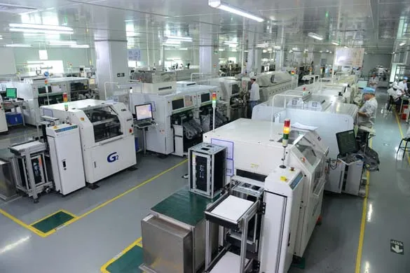
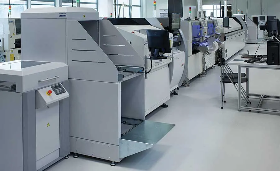
This includes the cost of drilling, etching, plating, and other processes to create the circuit patterns and layers. Complexity and the number of layers directly influence these costs. - Assembly Costs
Costs associated with placing components onto the PCB, including manual or automated pick-and-place processes, soldering and component costs. - Testing Costs
Expenditure associated with electrical testing (e.g., flying probe, bed-of-nails), visual inspection, and other quality assurance procedures. - Tooling and Setup Fees
These are one-time costs for preparing the necessary tools and programs for your specific design. These costs are often higher for smaller production runs but are spread out over larger volumes, reducing the per-unit cost.
| Cost Factor | Description | Impact on Cost |
|---|---|---|
| Number of Layers | Number of conductive layers in the PCB | Directly proportional; more layers, higher cost |
| Material Type | Type of substrate used for the PCB | Variable; advanced materials significantly increase costs |
| Board Size | Physical dimensions of the PCB | Larger boards require more material, increasing costs |
| Minimum Trace Width and Spacing | Small traces and gaps increase manufacturing complexity | Increased cost, higher precision required |
| Number of Holes and Vias | Number of drilled holes and vias | Increased cost with more features |
| Surface Finish | Type of finish applied (e.g. HASL, ENIG, Immersion Tin, OSP) | Variable; ENIG generally more expensive than HASL |
| Quantity | Number of PCBs manufactured in a batch | Per-unit cost decreases with higher quantities due to economies of scale |
It is important to note the interplay between these factors. For instance, while a simpler 2-layer PCB design is less expensive to produce, requirements for a high density design will increase both material and fabrication costs. High-precision requirements will also influence the type of PCB factory you select, as not all factories can handle these requirements. Working with a reputable [pcb factory] will help to give realistic cost estimates to avoid over or under budget.
Frequently Asked Questions About PCB Manufacturing
This section addresses common questions regarding PCB manufacturing, offering clarity on fundamental concepts and processes. These questions are crucial for anyone involved in electronics design and production, providing a foundation for understanding how to navigate the complexities of printed circuit board fabrication.
- What does PCB stand for in manufacturing?
PCB stands for Printed Circuit Board. It's a foundational component in electronics, serving as the base for mounting and connecting electronic components. - Where are most PCBs manufactured?
A significant portion of global PCB manufacturing occurs in Asia, particularly in China, due to its manufacturing capacity and cost advantages. However, there are also PCB manufacturers located across the world, including North America and Europe, often specializing in smaller batches, high technology products or local supply chains. - What are the main steps in the PCB manufacturing process?
The PCB manufacturing process generally includes: design and layout, creating the film layers, etching the copper layers, drilling holes, plating, solder mask application, silkscreen printing and final testing. Each step requires precision and is critical for the proper functioning of the final PCB. - What is the difference between single-sided, double-sided, and multilayer PCBs?
Single-sided PCBs have conductive material (usually copper) on only one side, double-sided have copper on both sides and multilayer PCBs have three or more layers of copper separated by dielectric material. Multilayer PCBs allow for more complex designs and higher densities of circuit connections. - How does a PCB factory handle prototyping?
PCB prototyping usually involves a streamlined process with faster turnaround times. PCB factory offer prototype services with small quantities, and may use different processes than large volume manufacturing. This approach allows for design validation and iterative improvements before mass production. - What certifications should a reputable PCB factory have?
A reputable PCB factory should possess certifications such as ISO 9001 for quality management, UL certification for safety standards and specific certifications such as IATF 16949 for the automotive industry and IPC standards, which define the industry wide standards of PCB design and manufacturing. These certifications ensure adherence to quality control and industry norms. - What factors affect PCB cost?
The cost of PCB is influenced by multiple factors including the number of layers, material type, board dimensions, hole size and the complexity of the board design, as well as the volume of production. Special surface finishes, controlled impedance, and tighter tolerances also impact the cost.
Comparing Top PCB Factory Capabilities
Selecting the right PCB factory hinges on a detailed comparison of their capabilities, encompassing the materials they handle, the technologies they employ, and their production timelines. This section provides an in-depth look at these critical factors to aid in a well-informed decision.
To facilitate a clear comparison, we'll examine a few representative examples of PCB manufacturers, highlighting their strengths and specializations. Note that specific capabilities may vary depending on factory updates and specific requests, so always confirm directly with the manufacturer for your unique project.
| PCB Factory | Materials Supported | Technology Focus | Typical Turnaround Time (Prototyping) | Production Volume Focus |
|---|---|---|---|---|
| JLCPCB | FR-4, Aluminum, Flexible PCBs | Rapid Prototyping, SMT Assembly | 2-5 Days | Small to Medium |
| PCBWay | FR-4, Rogers, Metal Core PCBs | High Layer Count PCBs, Advanced Materials | 3-7 Days | Small to Large |
| Eurocircuits | FR-4, IMS, Rigid-Flex | High Mix, Low Volume, Specialized Designs | 5-10 Days | Small to Medium |
| Advanced Circuits | FR-4, Rogers, Polyimide | Quick-Turn, High Reliability Boards | 1-3 Days | Small to Medium |
| Kingboard Chemical Holdings | Extensive range including FR-4, CEM-1, and specialty laminates | High-volume, mass production | Variable, typically longer | Large Volume |
This table provides a high-level overview. A more detailed analysis should consider the specific needs of your project. For example, a project requiring high-frequency performance might prioritize a factory with expertise in Rogers materials, while a rapid prototyping effort may focus on turnaround time and cost for small quantity.
- Material Capabilities
Consider which materials are supported. Standard FR-4 is suitable for many applications but specialized substrates are needed for high frequency or thermal management. - Technology Focus
Some factories specialize in high layer count PCBs, microvias, or particular assembly methods (e.g., SMT, through-hole). - Turnaround Time
The time required to manufacture and deliver the PCBs; varies based on complexity and production volumes. - Production Volume
Consider factories tailored for prototype, small batch, or large volume needs. The production capacity and pricing can vary widely across different factories.
Ensuring Quality Control and Reliability
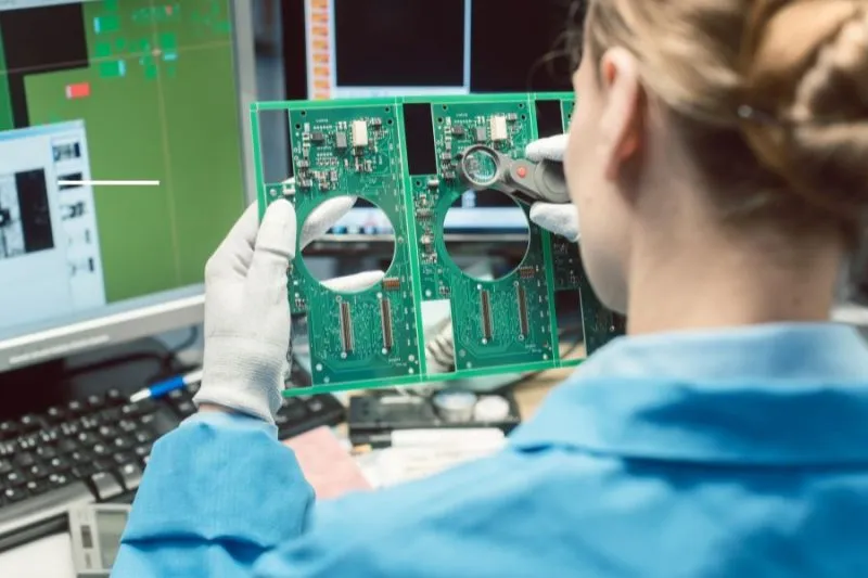
A reliable PCB factory employs rigorous quality control measures to ensure the consistent production of high-quality printed circuit boards. These measures encompass various stages of the manufacturing process, from raw material inspection to final product testing, and are vital for minimizing defects and ensuring the PCBs meet the required performance standards. A robust quality control system is not just about catching errors; it's about building in quality at every step.
Key aspects of a PCB factory's quality control and reliability include:
- Material Inspection:
Incoming raw materials, such as laminate and copper foil, are rigorously inspected for defects and compliance with specifications. This ensures the foundation of the PCB is of high quality. For example, a factory might use a copper foil thickness measurement device to verify the copper's exact thickness. - Automated Optical Inspection (AOI):
AOI machines use high-resolution cameras to automatically scan PCBs for defects such as shorts, opens, and missing features. This is typically done after etching and before soldermask application. This minimizes the likelihood of defects making it to the final product, such as missing drills or broken traces. - Electrical Testing:
Bare boards undergo electrical tests using a flying probe tester or bed-of-nails fixture to verify connectivity between all layers and components, catching faults such as open circuits or shorts that are not visually apparent. - X-Ray Inspection:
X-ray machines are used to inspect multilayer PCBs for internal defects such as misaligned vias or incomplete plating, especially useful for PCBs with complex inner layers and ball grid array (BGA) components. - Dimensional Accuracy Checks:
Precision measuring tools are used to verify the dimensions of the PCB and its features, like via placement and board thickness, to ensure it conforms to the design specifications. This is crucial to fit within the final product. - Controlled Impedance Testing:
For high-speed PCBs, controlled impedance testing using Time-Domain Reflectometry (TDR) validates that signal traces are designed correctly to minimize signal reflections and interference. This ensures the performance of high-speed digital or RF designs. - Solderability Testing:
Solderability testing checks the capability of the final pads for effective soldering, ensuring that components can be reliably attached. This involves subjecting pads to controlled solder environments, inspecting results under a microscope and ensuring consistent surface tension. - Environmental Testing:
Some PCB factories may perform environmental tests such as thermal shock testing and humidity testing to ensure the reliability of the board in harsh operating conditions.
Furthermore, certifications like ISO 9001 demonstrate a factory's commitment to maintaining a quality management system, which is a standardized set of quality control procedures. UL certification, on the other hand, signifies that the product meets safety requirements. These certifications provide external validation of the PCB factory's adherence to quality standards.
| Testing Method | Purpose | Tools Used |
|---|---|---|
| Incoming Material Inspection | Verify the quality of raw materials | Calipers, Thickness Gauges, Microscopes |
| Automated Optical Inspection (AOI) | Detect surface defects and missing features | High-Resolution Cameras |
| Electrical Testing | Verify connectivity and identify shorts/opens | Flying Probe Tester, Bed-of-Nails Fixture |
| X-Ray Inspection | Inspect internal defects | X-Ray Machines |
| Dimensional Accuracy Checks | Verify the PCB's dimensions | Precision Measuring Tools |
| Controlled Impedance Testing | Validate signal trace impedance | Time-Domain Reflectometry (TDR) |
| Solderability Testing | Test the pads for solder effectiveness | Solder Baths, Microscopes |
| Environmental Testing | Test durability in harsh conditions | Thermal Shock Chambers, Humidity Chambers |
By implementing these rigorous testing and certification processes, a reputable PCB factory ensures that it delivers reliable, high-performance circuit boards, minimizing the risk of field failures, and ensuring overall customer satisfaction. Choosing a factory that invests in these robust systems is crucial for the long-term success of any electronic product.
The Future of PCB Manufacturing
The printed circuit board (PCB) industry is undergoing significant transformation driven by advancements in materials, design methodologies, and manufacturing processes. These innovations are not just incremental improvements, but represent a paradigm shift in how PCBs are conceived, fabricated, and integrated into electronic devices. Leading PCB factories are at the forefront of these changes, pushing the boundaries of what's possible in electronics manufacturing.
Here's a detailed look into the trends shaping the future of PCB Manufacturing:
- Advanced Materials
The demand for high-performance electronics is driving the adoption of new substrate materials with improved thermal, mechanical, and electrical properties. These include advanced polymers, ceramics, and composites that offer higher operating temperatures, lower dielectric constants, and better signal integrity. These materials enable the design of more robust and efficient electronic devices. For example, the use of nanomaterials in PCB fabrication is enhancing conductivity and reducing the size of circuit elements. - Additive Manufacturing
Additive manufacturing, also known as 3D printing, is revolutionizing PCB fabrication. This technology enables the creation of highly complex PCB geometries and customized layouts, reducing material waste and production lead times. This is especially useful in prototyping and creating small batches of specialized PCBs. It also allows for more intricate designs that were previously difficult or impossible to achieve with traditional methods. Leading PCB factories are investing in additive manufacturing technologies to improve their rapid prototyping services. - High Density Interconnect (HDI)
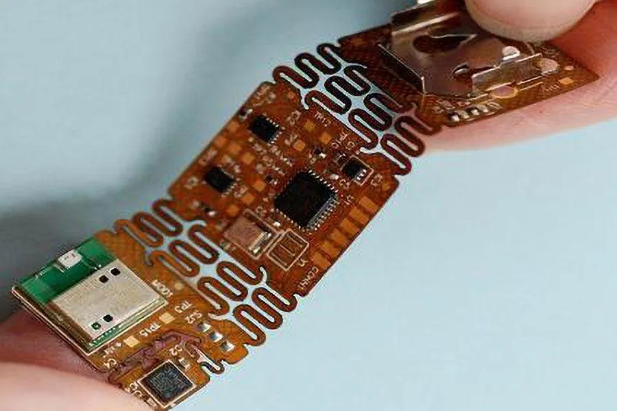
The trend towards miniaturization of electronic devices requires PCBs with smaller feature sizes and higher interconnect density. HDI technology enables the creation of PCBs with microvias, finer lines, and tighter spacing, allowing for more complex circuitry in a smaller footprint. As devices become more compact, HDI PCBs are crucial for enabling dense packaging and improving functionality within constrained spaces. PCB factories are constantly improving their HDI manufacturing capabilities to meet these demands. - Flexible and Stretchable PCBs
Flexible PCBs, made from flexible substrates, are increasingly used in wearable electronics and medical devices due to their ability to conform to curved surfaces and withstand flexing. Further advancements in stretchable substrates are opening up new opportunities for the development of truly wearable and implantable electronic devices. These flexible and stretchable PCBs are designed to move and flex with the body, allowing for innovative applications in health monitoring, smart textiles, and other emerging fields. PCB manufacturers are actively developing new techniques to produce these advanced substrates efficiently and cost-effectively. - Sustainable Manufacturing
Environmental sustainability is becoming a critical consideration in the PCB industry. There's a growing push towards the use of eco-friendly materials, waste reduction, and energy-efficient manufacturing processes. This includes recycling and recovering valuable metals and reducing the consumption of hazardous chemicals. PCB factories are implementing new techniques to reduce their environmental footprint and to provide sustainable products. The adoption of these practices not only benefits the environment but also provides a competitive advantage in the market. - Automated Manufacturing
Automated manufacturing processes using AI and robotics are improving production efficiency, reducing human error, and ensuring higher levels of consistency. From automated assembly lines to sophisticated testing, technology is helping PCB factories achieve higher throughput, improved accuracy, and lower costs. Smart factories leveraging Industry 4.0 concepts are quickly becoming the standard, and this trend is further reducing the need for human intervention in repetitive and less complex tasks. PCB manufacturers are investing in these technologies to improve their production capability and competitiveness. - Embedded Components
Embedding passive and active components directly into the PCB layers leads to increased component density, reduced assembly costs and improved electrical performance. It helps to minimize parasitic effects and to achieve better thermal management by distributing the heat more efficiently within the PCB structure. The use of embedded components is also helpful in making the final devices more compact. PCB factories are constantly developing new methods for incorporating these components into PCBs.
Leading PCB factories are not just adopting these trends, but they are actively driving them, by investing in research and development of new materials, processes and technologies, they are shaping the future of PCB manufacturing. This forward-thinking approach ensures that they remain at the cutting edge of the electronics industry.
Selecting the right PCB factory is paramount for bringing your electronic innovations to life. By carefully considering the factors outlined in this guide, you can secure a reliable partner who can consistently deliver high-quality PCBs. Whether it's a small prototype run or a large production order, the capabilities of your chosen [pcb factory] will directly impact your project's success. With continuous technological advancement, PCB manufacturing is constantly evolving, requiring businesses to stay informed and make strategic choices to achieve optimal results.