Choosing the Right Printed Circuit Board Factory: A Comprehensive Guide
Printed circuit boards (PCBs) are the backbone of modern electronics, silently powering everything from smartphones to industrial machinery. Choosing the right printed circuit board factory is crucial for ensuring the quality and reliability of your electronic devices. This guide will walk you through the key factors to consider when selecting a PCB manufacturing partner, helping you understand the intricacies of PCB production and making the best choice for your project.
Types of Printed Circuit Board Factories: A Comparative Overview
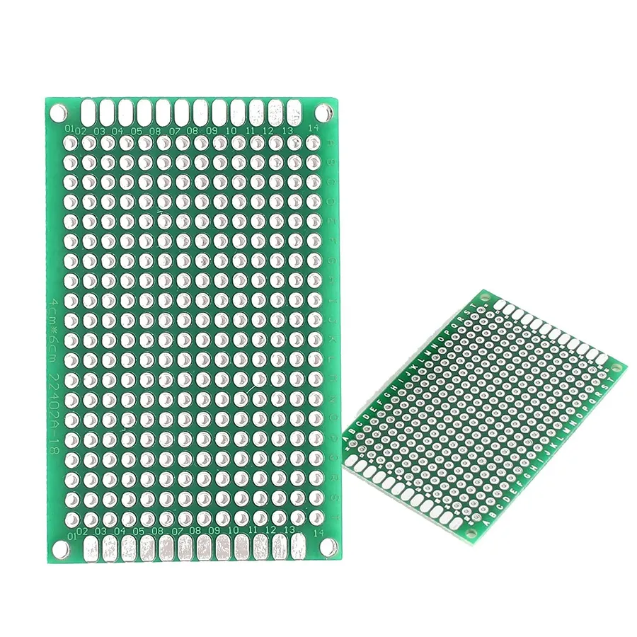
Printed circuit board (PCB) factories vary significantly in their focus and capabilities, each catering to different production needs. Understanding these variations is crucial for selecting the right partner for your project. This section provides a comparative overview of different types of PCB factories, including prototype-focused, high-volume production, and specialized manufacturers.
| Factory Type | Focus | Strengths | Weaknesses | Ideal For |
|---|---|---|---|---|
| Prototype-Focused | Small quantities, quick turnaround | Fast lead times, design flexibility, lower setup costs | Higher per-unit cost, limited large-scale capabilities | Initial design verification, small batch testing, rapid iteration cycles |
| High-Volume Production | Large quantities, cost efficiency | Economies of scale, standardized processes, lower per-unit cost | Longer lead times for initial setup, less flexibility in design changes | Large scale product manufacturing with established design |
| Specialized Manufacturers | Specific technologies or materials | Expertise in advanced technologies (e.g., flexible PCBs, HDI), use of unique materials. | Higher costs, limited availability, specific equipment needs | Projects requiring special technologies, materials, or certifications |
Key Factors in Choosing a Printed Circuit Board Factory
Selecting the right printed circuit board (PCB) factory is crucial for the success of any electronics project. This decision hinges on several key factors that directly impact cost, quality, and time-to-market. A thorough evaluation of these elements will ensure a suitable partnership that aligns with your specific requirements and project goals.
| Factor | Description | Importance |
|---|---|---|
| Cost | The price per PCB, including tooling and setup costs. Consider both unit price for high-volume and cost for low-volume prototyping. | Critical for budgeting, especially for startups and cost-sensitive products. |
| Manufacturing Capability | The factory's ability to handle your specific PCB design, including layer count, materials, and special features. | Essential for ensuring the factory can produce PCBs that meet your technical requirements. |
| Production Speed | The time it takes for a factory to produce and deliver your PCBs. Lead times are crucial for project scheduling. | Key for meeting deadlines and rapid product development cycles. |
| Quality Control Measures | The factory's processes for ensuring the quality and reliability of PCBs, including inspections and testing. | Vital for ensuring the performance and reliability of your end product. |
| Geographic Location | The factory's location can affect shipping times, costs, and communication. Consider domestic versus overseas options. | Important for logistics, communication, and potential legal and geopolitical factors. |
| Customer Service | The level of support and communication provided by the factory during the entire process. | Necessary for efficient collaboration and issue resolution. |
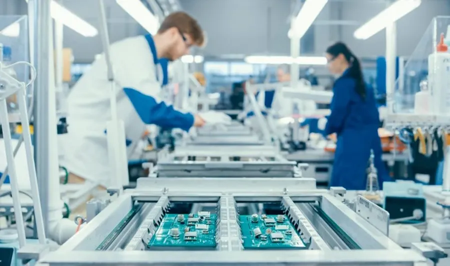
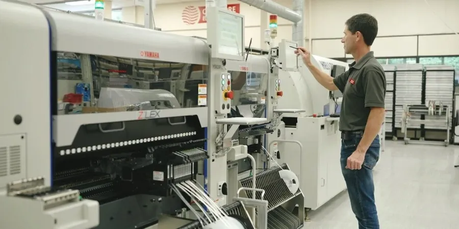
The PCB Manufacturing Process: From Design to Delivery
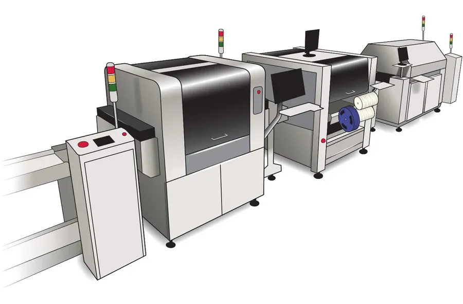
The fabrication of a printed circuit board (PCB) is a complex, multi-stage process that transforms a design concept into a tangible electronic component. This process encompasses design review, material preparation, pattern transfer, copper etching, hole creation, layer stacking, plating, solder mask application, component identification printing and final inspection.
- Design Review and Preparation
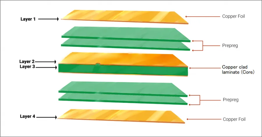
The process begins with a thorough review of the PCB design files, typically in Gerber format. Engineers verify the design's manufacturability (DFM), identifying potential issues and ensuring alignment with factory capabilities. Following the review, CAM (Computer-Aided Manufacturing) software converts the design into instructions for the production equipment. Materials, such as copper-clad laminates, are selected and prepared based on design specifications. - Imaging and Pattern Transfer
A photo-sensitive dry film is applied to the copper-clad laminate. The PCB design patterns are then transferred onto this film using UV light exposure through a photomask. The exposed areas of the photoresist harden, protecting the underlying copper during the subsequent etching process. - Etching
In the etching process, the unexposed photoresist is removed, and the copper not protected by the hardened resist is chemically dissolved. This process defines the conductive traces and pads of the PCB. Etching must be carefully controlled to achieve accurate line widths and spacing. The etching process uses ferric chloride or cupric chloride to remove the unwanted copper. - Drilling
Following etching, holes are drilled using precision CNC drilling machines. These holes are for component mounting, vias (interlayer connections), and mounting hardware. The drilling process uses very accurate computer-controlled machines and different drill bit sizes are used based on the design requirements. - Plating
Once drilling is complete, the PCB undergoes a plating process to enhance conductivity and enable reliable soldering. This involves electroless plating of copper followed by electrolytic plating, which builds a layer of copper on the walls of the drilled holes and the surface of the board to ensure reliable connections. This copper layer is typically plated with tin or gold as a protective layer. - Solder Mask Application
A layer of solder mask is applied to the PCB, defining areas that should not be soldered. This is typically an epoxy resin with color that is applied on the board, this prevents the occurrence of shorts when components are soldered to the PCB and is done with a photographic process. - Component Identification Printing
Component identification markings, logos and other relevant information are printed onto the PCB using a silk screen process. This printing process uses an epoxy based ink and provides clear and concise information, aiding during assembly. - Final Inspection
The completed PCBs undergo a final inspection that includes both visual and electrical tests. Visual inspection ensures that there are no defects in etching, plating, and solder mask application and that all component markings are present. Electrical testing checks for continuity and isolation to ensure that the PCB is functional. Boards that pass inspection are prepared for delivery.
Critical Certifications and Standards for PCB Factories
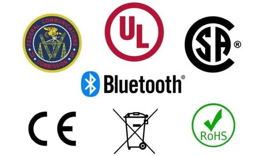
Adherence to industry certifications and standards is paramount for printed circuit board (PCB) factories to ensure consistent quality, reliability, and performance. These certifications demonstrate a factory's commitment to rigorous processes and help build trust with clients seeking high-quality PCBs.
| Certification/Standard | Description | Significance for PCB Manufacturing |
|---|---|---|
| ISO 9001 | An international standard that specifies requirements for a quality management system (QMS). | Ensures that the PCB factory has well-defined processes for all stages of manufacturing, from design review to final inspection. It focuses on customer satisfaction and continuous improvement. |
| AS9100D | A quality management standard for the aerospace industry, building upon ISO 9001 with additional requirements specific to this sector. | Critical for PCB factories serving the aerospace and defense sectors. It mandates strict process control, risk management, and traceability to meet the stringent requirements of these industries. |
| IPC Standards (e.g., IPC-A-600, IPC-6012, IPC-A-610) | Standards developed by the IPC (Association Connecting Electronics Industries) that establish accepted practices for PCB manufacturing. | Define acceptable quality levels, performance characteristics, and reliability guidelines for various PCB types. Ensures consistency in materials, processes, and inspection criteria. |
| UL Certification | Certifications from Underwriters Laboratories, a global safety science company. | Indicates that the PCB materials and manufacturing processes meet specific safety and performance requirements, essential for products used in regulated industries. |
| RoHS Compliance | Restriction of Hazardous Substances Directive of the European Union. | Ensures that PCBs are produced without the use of hazardous materials such as lead, mercury, cadmium and hexavalent chromium, contributing to environmental protection and compliance with regulations |
| REACH Compliance | Registration, Evaluation, Authorisation and Restriction of Chemicals, a European Union regulation. | Ensures that PCB manufacturing processes do not use substances harmful to human health and the environment. |
Beyond these core standards, some PCB factories may also pursue industry-specific certifications or undergo regular audits by their clients. The presence and relevance of specific certifications will depend on the target market for the PCBs produced. Selecting a PCB manufacturer with relevant and up-to-date certifications is crucial for ensuring quality and minimizing the risks associated with defective boards.
Prototype PCB Manufacturing vs. Mass Production
Printed circuit board (PCB) manufacturing processes diverge significantly between prototyping and mass production, each requiring distinct approaches and considerations. Understanding these differences is crucial for selecting the appropriate manufacturing strategy for your project's phase and volume requirements.
| Feature | Prototype PCB Manufacturing | Mass Production PCB Manufacturing |
|---|---|---|
| Purpose | Validation of design, functionality, and materials | Large-scale replication of a finalized and tested design |
| Volume | Low volume, often ranging from a few units to small batches | High volume, ranging from thousands to millions of units |
| Lead Time | Typically faster lead times due to lower complexity and volume | Longer lead times due to higher volume and more complex logistics |
| Cost per Unit | Higher unit cost because of setup costs and smaller quantities | Lower unit cost due to economies of scale |
| Process Flexibility | More flexibility for design changes and experimentation | Less flexibility due to standardized and optimized processes |
| Equipment and Tooling | Uses more general-purpose equipment and may require manual handling | Utilizes specialized, high-throughput equipment and automated processes |
| Quality Control | Rigorous testing for each prototype to identify any design flaws | Statistical process control to maintain consistent quality across large volumes |
| Material Selection | May involve a wider range of materials and customized options | Focuses on a limited selection of cost-effective materials |
Prototype PCB manufacturing is characterized by its focus on design validation and flexibility. It often involves a close collaboration between the design team and the manufacturer, allowing for quick iterations and modifications. The emphasis is on rapidly producing a small batch of boards to verify functionality and performance before committing to larger production runs. Mass production, on the other hand, prioritizes efficiency and cost-effectiveness. It uses highly optimized processes, automated machinery, and statistical quality control to deliver large volumes of consistent, high-quality PCBs. The process is less flexible, but it is essential for scaling up successful prototypes.
Geographic Considerations: Domestic vs. Offshore PCB Factories
The decision between selecting a domestic or offshore printed circuit board (PCB) factory is a critical one, impacting cost, lead times, communication, and logistics. This section provides a balanced analysis of these factors to guide your choice.
| Factor | Domestic PCB Factories | Offshore PCB Factories |
|---|---|---|
| Cost | Higher unit cost due to labor, infrastructure, and regulatory compliance. | Lower unit cost due to lower labor costs and economies of scale. |
| Lead Time | Shorter lead times, especially for prototypes and smaller production runs, due to proximity. | Longer lead times due to shipping and customs clearance, especially during peak seasons. |
| Communication | Easier communication due to similar time zones, language, and cultural norms, facilitating quicker feedback and issue resolution. | Potential communication challenges due to time zone differences, language barriers, and cultural differences. |
| Logistics | Simpler logistics due to lower shipping distances and less complex customs procedures. | More complex logistics involving international shipping, customs duties, and potential delays. |
| Intellectual Property (IP) Protection | Stronger IP protection due to established legal frameworks and enforcement mechanisms. | Potential risks of IP infringement due to differences in legal systems and enforcement. |
| Quality Control | Often easier to conduct on-site quality inspections and audits due to physical proximity, but not always guaranteed. | May require more stringent processes for quality assurance, and may be challenging to conduct in person audits. |
| Minimum Order Quantity (MOQ) | Generally lower MOQ, can be flexible for prototypes. | Typically higher MOQ, which can be a barrier for small projects or prototyping. |
Frequently Asked Questions about Printed Circuit Board Factories
This section addresses common queries regarding printed circuit board (PCB) factories, offering concise and authoritative answers to clarify prevalent questions within the industry. We aim to provide clarity on manufacturing locations, leading manufacturers, and specific company details.
- Where are most printed circuit boards manufactured?
The majority of printed circuit boards are manufactured in Asia, particularly in China, Taiwan, and South Korea. These regions have established robust supply chains and offer competitive manufacturing costs, making them global hubs for PCB production. However, there are also significant manufacturing facilities in North America and Europe. - Who is the largest PCB manufacturer in the USA?
While the PCB manufacturing landscape is dynamic, companies like TTM Technologies and Sanmina are often cited as some of the largest PCB manufacturers in the USA, based on revenue and manufacturing capacity. However, this can vary based on specific market sectors and metrics. - How to set up a PCB manufacturing factory?
Setting up a PCB manufacturing factory requires significant capital investment, technical expertise, and meticulous planning. Key elements include securing a suitable facility, acquiring specialized machinery (e.g., imaging, etching, plating equipment), establishing a reliable supply chain for raw materials, and implementing rigorous quality control processes. Additionally, compliance with environmental and safety regulations is crucial, as well as a skilled labor force. - Is JLCPCB a Chinese company?
Yes, JLCPCB is a PCB manufacturing company based in China. They are known for offering low-cost PCB prototyping and manufacturing services, and have a global customer base. They are based in Shenzhen. - What are the typical lead times for PCB manufacturing?
Lead times for PCB manufacturing can vary significantly based on the complexity of the board, the manufacturing process used, and the location of the factory. For simple prototypes, lead times can be as short as a few days, while complex or high-volume orders may take several weeks. Domestic manufacturers may offer faster lead times but at a higher cost, while offshore production is typically less expensive but takes longer. - What quality control measures should a good PCB factory have?
A reputable PCB factory will employ rigorous quality control measures at every stage of the manufacturing process. This includes incoming material inspection, in-process checks at each production step, and final testing which may include electrical testing, functional testing, and visual inspection. Furthermore, certifications like ISO 9001 or AS9100D indicate a commitment to quality. - How do PCB factories handle intellectual property (IP) protection?
Protecting intellectual property is paramount. Many PCB factories use non-disclosure agreements (NDAs) and have internal procedures in place to maintain client confidentiality. It is critical to work with reputable manufacturers and confirm their IP protection policies in advance. Thorough due diligence and clear contract terms provide the best safeguards.
Practical Tips for Collaborating with a Printed Circuit Board Factory
Effective collaboration with a printed circuit board (PCB) factory is crucial for a successful project. This involves clear communication, adherence to design guidelines, and a well-defined request for quote (RFQ) process. By following these practical tips, you can streamline the manufacturing process, reduce errors, and ensure your PCBs are fabricated to your specifications.
- Design for Manufacturability (DFM) Guidelines
Adhere strictly to the PCB factory's DFM guidelines. These are essential to avoid design flaws that could lead to manufacturing issues. This includes minimum trace widths, spacing, and via sizes, among others. Always review and implement the specific DFM rules of your chosen factory, as these can differ between manufacturers. Ignoring DFM can lead to increased costs and delays. - Clear and Concise Communication
Maintain clear and concise communication with the PCB factory from the start. Provide comprehensive and accurate design files, BOMs (Bill of Materials), and detailed instructions. Use professional language and avoid jargon that might be ambiguous. Regular and open communication allows for quick resolution of any queries or problems that may arise. Using a defined communication channel or a project management tool can help centralize conversations and file sharing. - Comprehensive Requests for Quotes (RFQs)
A well-structured RFQ is vital for accurate quotes and to avoid hidden costs. It should include detailed specifications, such as the board dimensions, layer count, material type, surface finish, and required quantities. Also specify any special requirements, testing needs, or packaging expectations. The more detailed your RFQ, the more accurate the quote will be, and the smoother the process will be. Including an estimated delivery timeline is also essential for planning. - File Formats and Documentation
Provide your PCB design files in the correct formats (e.g., Gerber, ODB++). Ensure that all design files, including schematics, layouts, and drill files, are well-organized and accurate. Include all necessary documentation, such as assembly drawings, and any specific testing requirements. Accuracy and completeness in file delivery reduces the likelihood of misinterpretation and delays in the manufacturing process. - Understanding Material Choices and Specifications
Be knowledgeable about the materials the PCB factory offers and understand the trade-offs between cost and performance. Ensure that the material chosen meets the requirements of the intended application, including thermal, electrical, and mechanical properties. Provide specific material specifications in your RFQ, including the copper thickness, substrate type, and solder mask options. Having a good understanding of material choices will enable you to make the right decisions. - Early Engagement
Engage with the PCB factory early in the design process, not just when you're ready to submit files. This allows for collaborative design reviews and allows the factory to provide valuable input on your design that can make it more manufacturable. Early engagement can also help you avoid costly redesigns and ensure the manufacturability of the final product. - Regular Updates and Progress Tracking
Establish regular communication updates with the factory, so that you can stay informed about the production progress and any potential issues that may arise. Have mechanisms in place to track the progress of your order, from the initial file submission to the final delivery. Early detection and resolution can minimize any potential disruptions to production schedules.
Future Trends in PCB Manufacturing
The printed circuit board (PCB) manufacturing industry is undergoing significant transformation, driven by advancements in materials, processes, and technologies. These trends are reshaping how PCBs are designed, fabricated, and integrated into electronic devices, impacting the operations of PCB factories profoundly.
- Flexible PCBs (Flex PCBs)
Flexible PCBs are gaining popularity due to their ability to conform to irregular shapes and fit into tight spaces, which is crucial for wearable electronics, automotive applications, and medical devices. These PCBs use flexible substrates like polyimide, enabling dynamic and complex designs. - High-Density Interconnect (HDI) Boards
HDI boards feature finer lines, smaller vias, and higher connection density, allowing for more functionality in a smaller form factor. This trend is essential for smartphones, tablets, and other compact electronic devices where space is at a premium. Manufacturers are adopting advanced technologies like laser drilling and microvia formation to produce these intricate boards. - Sustainable Manufacturing Practices
Environmental consciousness is pushing PCB factories towards sustainable practices. This includes using eco-friendly materials, reducing water consumption, minimizing waste, and adopting energy-efficient processes. Regulations and customer preferences are driving this shift towards greener manufacturing. - Additive Manufacturing for PCBs
Additive manufacturing (3D printing) is emerging as a viable alternative to traditional PCB fabrication methods, particularly for prototyping and custom designs. This approach enables quicker turnaround times and more complex geometries without the need for tooling, reducing costs and lead times, and promoting on-demand manufacturing - Embedded Components
Embedding components directly into the PCB substrate is a trend that reduces the overall size and weight of electronic devices while improving signal integrity. This technique enables higher integration and improved reliability, which is essential for high-performance electronics. Specialized materials and processes are needed to achieve the precise placement and encapsulation of components. - Smart Factories and Automation
The adoption of Industry 4.0 principles, including automation, data analytics, and IoT, is transforming PCB factories into smart facilities. Automated assembly lines, predictive maintenance, and real-time monitoring are optimizing production processes, reducing costs and errors, and improving the overall efficiency and quality control.
Choosing the right printed circuit board factory is a critical decision that can significantly impact the success of your electronic product. By carefully considering factory types, manufacturing capabilities, certifications, and geographic location, you can select a partner that meets your specific needs and ensures the quality and reliability of your PCBs. As technology evolves, staying informed about industry trends will further help you make informed decisions in the future. With a trusted PCB factory at your side, your projects can be brought to life with confidence.