Decoding Bluetooth PCB Board Prices: A Comprehensive Guide
In our increasingly wireless world, Bluetooth technology is integral, and at the heart of every Bluetooth device lies a crucial component: the PCB board. But how much does a bluetooth PCB board cost? The price can vary dramatically based on complexity, production volume, and features. Let's delve into the world of Bluetooth PCBs, exploring the intricate factors behind their pricing to help you navigate the market with confidence.
Understanding the Basics of Bluetooth PCB Boards
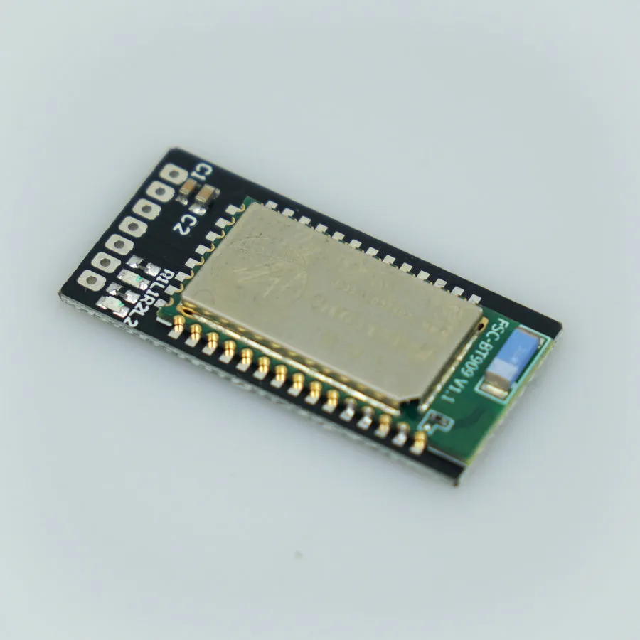
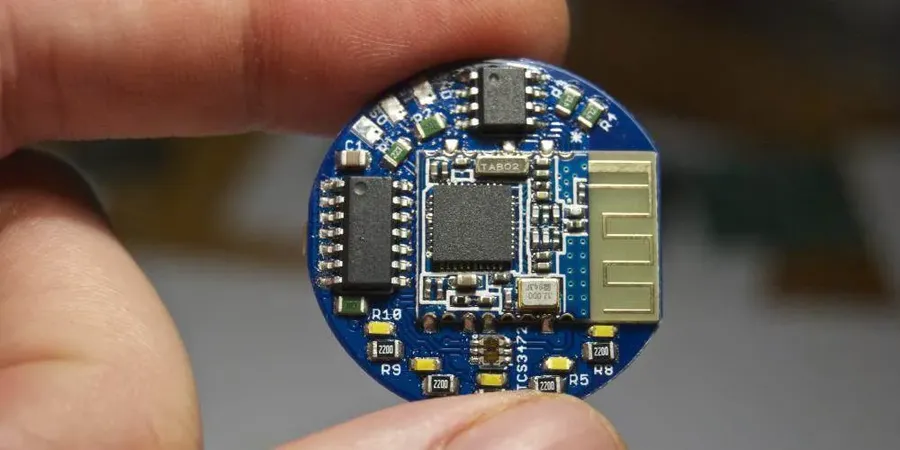
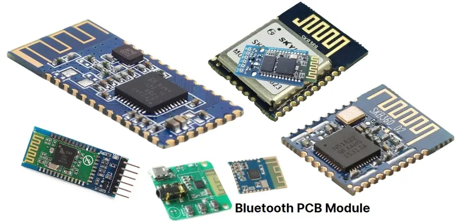
A Bluetooth PCB (Printed Circuit Board) is the foundational component enabling wireless communication via the Bluetooth protocol. It's a specialized board integrating electronic components, conductive pathways, and a Bluetooth module or chip, facilitating data exchange between devices over short distances. Without the PCB, Bluetooth functionality, as we know it, would not exist, underscoring its essential role in the world of wireless technologies.
Key Factors Influencing Bluetooth PCB Board Prices
The price of a Bluetooth PCB board is not fixed; it fluctuates based on several key factors. These factors encompass the materials used, the complexity of the board's design, its size, and the overall quantity being manufactured. A thorough understanding of these elements is crucial for anyone seeking to optimize costs without sacrificing quality.
| Factor | Description | Impact on Price |
|---|---|---|
| PCB Material | The substrate material of the PCB, such as FR-4, Aluminum, or flexible materials. | Higher performance materials (e.g., those with better thermal properties) typically increase cost. |
| Board Complexity (Layers) | The number of conductive layers in the PCB. Can range from single-layer to multi-layer (e.g., 2-layer, 4-layer, 6-layer, and above). | More layers increase manufacturing complexity and costs. Multi-layer boards are generally more expensive. |
| Board Size | The physical dimensions of the PCB. | Larger boards generally require more material and fabrication time, leading to increased costs. |
| Quantity | The number of PCBs ordered in a production run. | Larger quantities usually result in lower per-unit costs due to economies of scale. |
| Surface Finish | The coating applied to the PCB, e.g., HASL, ENIG, Immersion Silver. | Premium finishes like ENIG are more expensive but offer better reliability and solderability. |
| Via Type | The type of vias used to make connections between layers; blind, buried, or through-hole vias. | Complex vias add to processing time and cost, with buried and blind vias being more expensive. |
| Specialized Requirements | Features like controlled impedance, specific plating requirements, and tight tolerances. | These requirements can increase processing time and necessitate specialized equipment, which increases cost. |
Types of Bluetooth PCB Boards and Their Price Ranges
Bluetooth PCB boards exhibit a wide range of types, each with distinct characteristics and price points, primarily driven by their complexity and features. This section explores the common variations in PCB design, material, and Bluetooth version, directly impacting their cost.
| PCB Type | Description | Typical Applications | Price Range (USD per board) | Factors Affecting Price |
|---|---|---|---|---|
| Single-Layer PCB | Simplest PCB type with conductive layer on one side. Best for basic circuits. | Simple Bluetooth sensors, basic low-cost Bluetooth devices | $0.5 - $5 | Quantity, Material, Board Size, and Basic Functionality |
| Double-Layer PCB | Conductive layers on both sides, allowing more complex circuitry. | Simple Bluetooth modules, hobbyist projects, low-complexity Bluetooth applications | $2 - $10 | Layer Thickness, Hole Count, Material, and Complexity |
| Multi-Layer PCB (4 Layers) | More than two layers, interconnected using vias, for higher-density design. | Mid-range Bluetooth devices, industrial controllers, advanced sensors. | $10 - $30 | Number of Layers, Signal Integrity requirements, Trace Density, and Material |
| Multi-Layer PCB (6-8 Layers) | Includes power and ground planes, enabling complex routing and performance. | High-performance Bluetooth systems, complex data loggers, sophisticated wireless devices | $30 - $75 | High Layer Count, Trace Density, and Power requirements |
| Bluetooth 4.x PCB | Board designed with Bluetooth version 4.x (LE - Low Energy), offering lower power consumption. | Wearables, IoT devices, beacons, power-sensitive applications | $1 - $20 | Bluetooth Chipset, Additional Components, and complexity of the PCB Design |
| Bluetooth 5.x PCB | Board designed with Bluetooth version 5.x, featuring improved range and speed compared to older versions. | Modern Smart devices, high data rate devices, sophisticated wireless controls. | $2 - $30 | Bluetooth Chipset, Additional Components, High-Performance PCB materials, and complexity of the PCB Design |
Manufacturing Process and Its Impact on Cost
The cost of a Bluetooth PCB board is significantly influenced by its manufacturing process, which encompasses a series of intricate stages from design conception to final assembly. Each stage contributes to the overall price, with factors like complexity, precision, and material usage playing crucial roles.
The manufacturing process for a Bluetooth PCB can be broken down into several key steps, each with its own cost implications:
- Design and Layout
This initial phase involves translating the schematic into a physical board layout using specialized software. The complexity of the design, number of layers, trace density, and the use of specific design rules (like impedance control for high-frequency signals) all contribute to the cost. More complex designs with denser routing require more time and expertise to implement which increases overall cost. - Material Selection
The choice of substrate material (e.g., FR-4, aluminum, Rogers) impacts performance and cost. High-performance materials with superior thermal and electrical properties are more expensive. Factors such as material thickness and copper cladding also play a role in cost. - Fabrication
Fabrication of the bare PCB board involves several processes including: etching, drilling, plating, lamination and solder mask application. The use of automated production lines, the number of drilling operations, and the complexity of the lamination process all add to the fabrication cost. Finer traces and smaller drill hole size increase production cost due to increased complexity and precision. - Testing
Rigorous electrical testing of the bare boards is crucial to ensure functionality. Techniques like flying probe testing or bed-of-nails testing help identify manufacturing defects. The thoroughness of testing directly affects the yield, and therefore the final price. More complex test procedures such as impedance testing will further add to the cost. - Surface Finishing
Applying a surface finish such as HASL, ENIG, or Immersion Silver provides protection against oxidation and improves solderability. The type of finish chosen will impact both cost and board performance.
Each of these stages has an associated time, cost, and complexity which impacts the final cost of the Bluetooth PCB. Careful selection of fabrication parameters and proper design choices can mitigate cost increases within the production process.
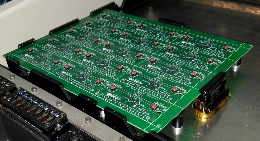
Bluetooth PCB Assembly (PCBA) Costs
Bluetooth PCB assembly (PCBA) costs represent a significant portion of the total expense associated with producing a functional Bluetooth-enabled device. This stage involves the physical mounting and soldering of electronic components onto the bare PCB, transforming it into a working circuit board. Understanding the various factors influencing PCBA costs is crucial for effective cost management and project planning.
The assembly process typically involves several key stages, each contributing to the overall cost:
- Component Sourcing
This involves procuring all the necessary electronic components, such as resistors, capacitors, integrated circuits (ICs), and the Bluetooth module itself. The cost of these components depends on factors such as their type, specifications, quantity, and the market demand at the time of purchase. Global chip shortages and fluctuations in raw material prices can significantly impact these costs. Using readily available and standardized parts where possible can help manage these expenses. - Solder Paste Application
Solder paste, a mixture of tiny solder particles and flux, is applied to the PCB pads where components will be mounted. The method of application, whether through a stencil or another process, impacts cost. Precision application is crucial for reliable connections. - Component Placement
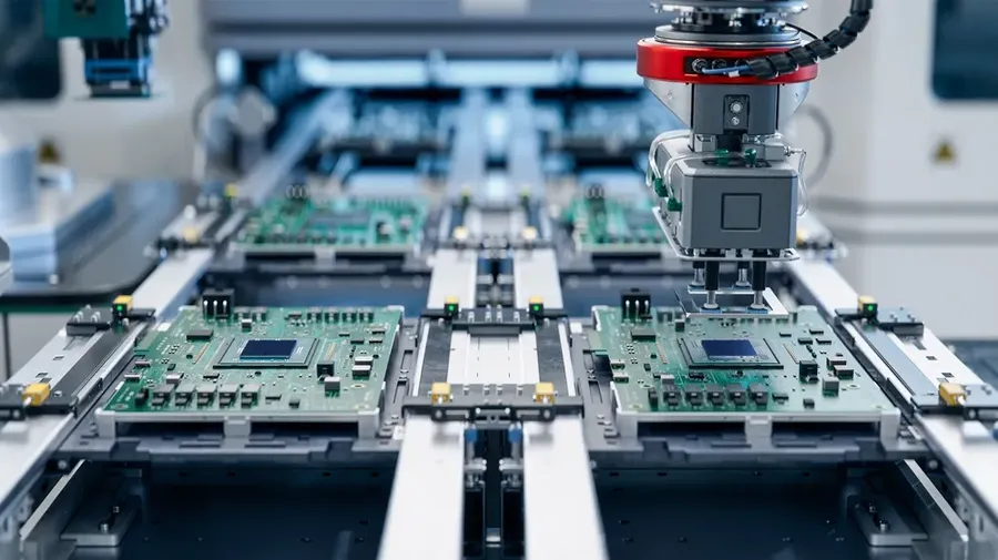
Automated machines are generally used to precisely position components onto the solder paste. The speed and accuracy of these machines influence assembly time and cost. More complex designs with numerous small components will drive up costs. - Soldering
The populated PCB is then passed through a reflow oven, which melts the solder paste, creating permanent electrical and mechanical connections between the components and the PCB pads. Different soldering techniques and equipment, such as wave soldering, will affect cost and production throughput. The type of solder used and specific temperature profiles also have cost implications. - Inspection and Testing
After soldering, the PCBA is inspected for errors such as misaligned components, solder bridges, and opens. This stage may involve manual inspection, automated optical inspection (AOI) and in-circuit testing (ICT). The level of testing and inspection rigor has a direct effect on the quality and reliability of the final product but increases cost and production time. Functional tests are also often performed to ensure that the PCBA operates as designed.
Labor costs are another critical factor in PCBA costs, especially for smaller production runs or those involving complex assembly or specialized testing. Automated assembly processes are essential for cost-effective volume production, whereas manual processes are sometimes necessary for small batch production.
Cost-Effective Strategies for Bluetooth PCB Board Production
Optimizing the cost of Bluetooth PCB board production requires a strategic approach that balances quality and affordability. Effective strategies involve design optimization, careful material selection, and smart vendor partnerships, all while maintaining the necessary performance and reliability.
- Design for Manufacturability (DFM)
Implementing DFM principles from the outset can significantly reduce production costs. This includes using standard component sizes, minimizing the number of layers, and optimizing component placement to reduce assembly time and complexity. - Panelization Strategy
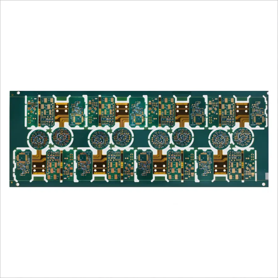
Efficient panelization involves arranging multiple PCBs on a single larger panel for fabrication, maximizing material utilization and streamlining the manufacturing process, leading to lower unit costs. - Component Selection
Selecting cost-effective components without compromising performance is crucial. Consider readily available parts and explore alternatives that offer similar functionalities at lower prices. - Optimize Layer Count
Reducing the number of layers in the PCB design simplifies the manufacturing process and reduces material costs. This is most effective when complex routing is not essential. - Vendor Selection
Choosing the right PCB manufacturer is paramount. Compare quotes from multiple suppliers, assessing their capabilities, turnaround time, and quality. Consider manufacturers with established expertise in Bluetooth PCB production. - Consider Alternative Materials
Explore less expensive PCB substrate materials that meet your performance requirements. While FR-4 is common, there may be suitable alternatives for specific use cases. - Quantity Matters
Larger production runs generally lead to lower per-unit costs. If possible, accurately forecast your demand to take advantage of volume discounts. - Negotiate with Suppliers
Build strong relationships with your suppliers and negotiate for better pricing and payment terms. Regular communication can lead to mutually beneficial agreements.
Bluetooth PCB Board Price Comparison: Suppliers and Marketplaces
Navigating the landscape of Bluetooth PCB board pricing requires a comparison across various suppliers and marketplaces. The cost can fluctuate significantly depending on the vendor, order volume, and manufacturing specifications. This section provides a comparative overview to assist in making informed purchasing decisions.
| Supplier/Marketplace | Typical Price Range (USD per board) | Lead Time | Minimum Order Quantity (MOQ) | Pros | Cons |
|---|---|---|---|---|---|
| Alibaba | $0.50 - $10.00+ | 2-8 weeks | Varies, often 100+ | Wide range of suppliers, competitive pricing, potential for customization. | Quality can vary significantly, longer lead times, higher MOQs, require careful vetting of suppliers. |
| eBay | $1.00 - $20.00+ | 1-4 weeks | Varies, often lower than Alibaba | Lower MOQs, good for prototyping or small batches, convenient buying process. | Limited customization options, inconsistent supplier quality, less control over manufacturing process. |
| Amazon | $2.00 - $30.00+ | 1-3 weeks | Varies, often lower than Alibaba | Fast shipping, reliable customer service, good for small quantities | Higher prices, limited selection, less customization options |
| Made-in-China | $0.75 - $12.00+ | 2-7 weeks | Varies, similar to Alibaba | Large range of suppliers, good for bulk orders, competitive pricing | Supplier quality varies, potential for longer lead times, require careful vetting of suppliers. |
| Specialized PCB Manufacturers | $5.00 - $50.00+ | 1-6 weeks | 1+ | Higher quality, advanced features available, more direct communication, customization options. | Higher cost, can require more technical know-how. |
Frequently Asked Questions About Bluetooth PCB Boards
This section addresses common queries about Bluetooth PCB boards, providing clear and concise answers to help you better understand their function, cost factors, and design considerations.
- What exactly is a Bluetooth PCB board?
A Bluetooth PCB (Printed Circuit Board) is the foundational component of any Bluetooth-enabled electronic device. It's a rigid board made of non-conductive material, typically fiberglass, upon which conductive pathways and components are mounted and interconnected. These components, including the Bluetooth chip, antennas, and supporting circuitry, enable wireless communication using the Bluetooth protocol. - Why are Bluetooth PCB boards sometimes so expensive?
The cost of a Bluetooth PCB board is influenced by multiple factors. These include the complexity of the board (number of layers), the type of materials used (such as high-performance laminates), the precision of the manufacturing process, the quantity ordered (economies of scale), and any specific design requirements, such as impedance control for signal integrity. Additionally, the inclusion of advanced features like impedance matching or specific antenna layouts can further elevate the price. - How do I begin designing a Bluetooth circuit for a PCB?
Designing a Bluetooth circuit requires a solid understanding of RF (Radio Frequency) principles, PCB layout, and the specific requirements of the Bluetooth chip being used. Start by selecting the appropriate Bluetooth module or chip. Then, carefully design the antenna and surrounding circuitry, adhering to the chip manufacturer's specifications. Using specialized PCB design software is essential, with attention paid to impedance matching, component placement, and signal routing to minimize signal loss and interference. Simulation tools can be utilized to verify your design before production. - Where can I find cost-effective options for Bluetooth PCB board production?
Cost-effective production options are usually achieved through strategic vendor selection and design optimization. Consider partnering with PCB manufacturers that offer competitive pricing for both prototype and volume production runs. For instance, manufacturers in regions with lower labor costs might offer better prices. Optimize your design to reduce unnecessary layers, use standardized components, and order in larger quantities to take advantage of economies of scale. Also, explore online marketplaces such as Alibaba, but conduct thorough research on vendor reliability and quality standards before placing an order. - What impact does the PCB layer count have on the final Bluetooth PCB price?
The layer count directly impacts the complexity and cost of a PCB. A higher layer count allows for more intricate routing and signal management, which is sometimes necessary for high-density and high-performance circuits such as those used for Bluetooth and RF designs. However, more layers mean higher material usage, longer manufacturing time and hence increase in cost. Simple Bluetooth applications might suffice with a two-layer or four-layer board, whereas more complex designs may necessitate six or more layers. Therefore, consider the functional requirements of the design against budget to select an appropriate layer count. - Are there specific PCB materials that can affect the price of a Bluetooth board?
Yes, the choice of PCB material can significantly affect the cost. Standard FR-4 material is the most common and generally more affordable, while materials like Rogers or Teflon, known for their superior electrical properties at higher frequencies, are more expensive. For Bluetooth applications, FR-4 is often sufficient unless specific needs such as very high frequency or low dielectric loss are present, which may require high-performance materials. Material selection requires balancing performance requirements with budgetary constraints. - How does the order volume of my Bluetooth PCB influence the per-unit price?
The per-unit price of PCBs drops considerably as the order volume increases, due to economies of scale. The initial tooling and setup costs for PCB production are fixed. Consequently, spreading these costs over a larger batch size results in a lower per-unit cost. Manufacturing costs including material procurement and machine setup are largely fixed regardless of the order volume, so a larger number of boards results in a reduced cost per unit. If your product has a large target market, plan ahead and order your PCBs in higher volumes to maximize cost savings.
Future Trends in Bluetooth PCB Board Pricing
The pricing landscape for Bluetooth PCB boards is not static; it's continuously evolving due to technological advancements, fluctuations in material costs, and the competitive dynamics of the industry. Anticipating these shifts is crucial for strategic planning and cost management.
Several key factors are expected to shape future pricing trends:
- Technological Advancements:
The relentless march of technology, particularly in chip manufacturing and material science, will likely lead to more efficient and cost-effective production methods. Innovations in PCB fabrication techniques, such as finer trace widths and higher layer counts, could initially increase costs but may eventually drive down prices as they become more widely adopted. - Material Costs:
Raw material prices for copper, FR-4, and other essential components can be volatile and significantly impact PCB board costs. Increased demand or supply chain disruptions can drive up prices, while advancements in material science might introduce more cost-effective alternatives. For example, the development of bio-based or recycled materials could lead to more sustainable and cheaper options. - Industry Competition:
The PCB manufacturing market is fiercely competitive, with numerous manufacturers vying for business. Increased competition will generally exert downward pressure on prices, particularly for standardized designs. However, specialized or high-performance boards may maintain premium pricing due to their higher complexity and niche applications. - Demand for Miniaturization:
The trend towards smaller, more compact electronic devices is pushing the limits of PCB technology. The demand for high-density interconnect (HDI) PCBs, which are more complex to manufacture, is rising, which could lead to price increases for some types of boards. However, as these technologies become mainstream, prices may eventually decrease. - Automation in Manufacturing:
Greater automation in PCB manufacturing processes, including automated assembly lines and AI-powered quality control systems, is anticipated to reduce labor costs and improve production efficiency, leading to potential price reductions. This trend is crucial for handling the growing complexity of PCB boards and faster turnaround times.
In the near term, we can expect to see a balancing act between the cost reductions from efficiency gains and the pressure from material and complexity demands. Manufacturers who embrace new technologies and optimize their supply chains will be best positioned to offer competitive pricing, while those who lag may face higher production costs. Ultimately, the market will dictate where pricing settles as these trends play out.
Understanding the bluetooth PCB board price involves considering a range of factors, from materials to assembly complexity. While costs can fluctuate, careful planning, strategic sourcing, and understanding your project requirements are crucial to achieving the best value. The future of wireless connectivity relies on these crucial components, and with the insights provided, you are better equipped to navigate the market and optimize your budget. Remember, investing wisely in quality materials and robust manufacturing processes will ultimately yield more reliable and cost-effective long-term solutions for your bluetooth-enabled products. Always consider long-term value, not just initial bluetooth pcb board price.