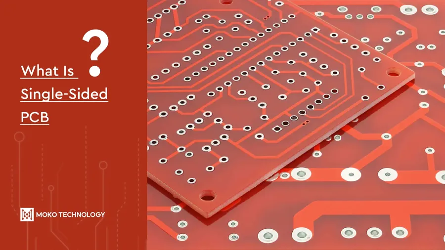
Double Sided PCB: Design, Applications & Manufacturing Guide

From smartphones to medical devices, the double sided PCB forms the backbone of countless electronic innovations. These boards, with conductive layers on both sides, enable complex circuits in compact spaces. This guide will demystify double sided PCB technology, covering its design, applications, and manufacturing, empowering you to harness its full potential.
What is a Double Sided PCB?
A double-sided printed circuit board (PCB) is characterized by having conductive copper layers on both the top and bottom surfaces of its insulating substrate. This design allows for increased circuit complexity and component density compared to single-sided PCBs. Key to this functionality are vias, which are plated-through holes that provide electrical connections between the two copper layers, enabling signal routing across both sides of the board. This foundational architecture is vital for modern electronics, facilitating intricate designs within compact spaces.
This section provides a concise comparison between single-sided and double-sided PCBs, highlighting their key differences in terms of complexity, cost, and application. Understanding these distinctions is crucial for selecting the appropriate PCB type for a given electronic design project.
| Feature | Single-Sided PCB | Double-Sided PCB |
|---|---|---|
| Copper Layers | One | Two |
| Circuit Complexity | Lower | Higher |
| Routing Flexibility | Limited | Increased with vias |
| Component Density | Lower | Higher |
| Cost | Lower | Slightly Higher |
| Manufacturing Difficulty | Easier | Slightly More Complex |
| Applications | Simple electronics, low-density circuits | More complex electronics, higher density circuits |
Double-Sided PCB vs. Single-Sided PCB
Double-sided PCBs represent a significant advancement over single-sided boards, primarily by incorporating conductive copper layers on both sides of the substrate. This fundamental design difference facilitates more intricate circuit layouts and allows for a higher density of components within a given area. The key enabling technology for this increased complexity is the use of vias, which establish electrical connections between the top and bottom layers.
The primary distinction lies in the conductive layer count. Single-sided PCBs have a single layer of copper on one side of the board, limiting routing complexity. Double-sided PCBs, however, feature a copper layer on both sides, enabling more versatile and intricate circuit designs. This design flexibility translates to more compact and capable electronics.
Single-Sided vs. Double-Sided PCB Comparison Table
| Feature | Single-Sided PCB | Double-Sided PCB |
|---|---|---|
| Conductive Layers | One | Two |
| Routing Complexity | Low | Higher |
| Component Density | Lower | Higher |
| Interlayer Connections | Not Applicable | Vias |
| Manufacturing Cost | Generally Lower | Generally Higher |
| Design Flexibility | Limited | Greater |
| Applications | Simple electronics, low-density circuits | More complex circuits, higher component density, various electronic devices |
Key Advantages of Double Sided PCBs
Double-sided PCBs offer significant advantages over their single-sided counterparts, primarily in terms of increased circuit density, enhanced signal routing capabilities, and greater design flexibility. These benefits stem from the presence of conductive layers on both sides of the substrate, allowing for more complex and efficient circuit designs.
- Increased Circuit Density
By utilizing both sides of the PCB for component placement and routing, double-sided boards can accommodate a higher number of components and interconnections within the same board area compared to single-sided PCBs. This is crucial for compact electronic devices. - Improved Signal Routing
The dual-layer structure facilitates more complex signal routing, including the use of vias to connect traces between layers. This reduces the length of traces and the potential for interference, resulting in more stable and reliable signal transmission. - Enhanced Design Flexibility
Double-sided PCBs provide designers with increased flexibility in component placement and trace routing. This allows for the creation of more sophisticated circuits and the optimization of board layout for performance and manufacturability. - Reduced Board Size
The ability to route on two layers, compared to the single layer of single sided PCBs, means that circuits with the same functionality can be designed on a smaller board. - Cost-Effective for Moderate Complexity
While more expensive than single-sided PCBs, double-sided boards strike a good balance between cost and performance for many applications where single layer is insufficient and multiple layers are not yet required.
Double Sided PCB Design Considerations

Designing double-sided PCBs requires careful consideration of several factors to ensure optimal performance, reliability, and manufacturability. These design considerations extend beyond single-sided PCBs, as the presence of two conductive layers allows for greater complexity, but also introduces new challenges related to signal integrity, thermal management, and fabrication constraints.
- Layout Planning
Careful arrangement of components and routing traces on both layers is essential. Efficient use of space, component orientation, and minimizing trace lengths are critical. Consider using CAD software tools for automated routing assistance. - Via Placement
Vias, which are conductive pathways that connect traces between the top and bottom layers, must be placed strategically. Proper via sizing and quantity are necessary for reliable electrical connections. Minimize vias in critical signal paths to reduce impedance discontinuities. - Impedance Control
In high-speed applications, controlling the impedance of signal traces is vital to maintain signal integrity. This involves carefully selecting trace widths, spacing, and dielectric materials, while considering the board's stack-up. Controlled impedance ensures minimal signal reflections and losses. - Thermal Management
Managing heat generated by components is crucial for reliability. Implement strategies like thermal vias, heat sinks, and proper component placement to facilitate heat dissipation. Consider airflow patterns in the final product and account for thermal limitations of components. - Layer Stack-up
The arrangement of copper layers and the insulating substrate affects impedance and signal transmission characteristics. Properly designed stack-ups can help improve signal quality. Ensure appropriate layer thickness and dielectric material to meet performance specifications. - Component Spacing and Clearance
Ensure adequate clearance between components, traces, and the board edge to avoid shorts and fabrication defects. Follow design rules for spacing to ensure reliable assembly and prevent solder bridges. Be mindful of tolerances during manufacturing. - Design Rule Check (DRC)
Use your PCB design software's DRC feature to check for layout errors and compliance with design rules before fabrication. These checks help identify errors like short circuits, missing connections, and inadequate spacing.
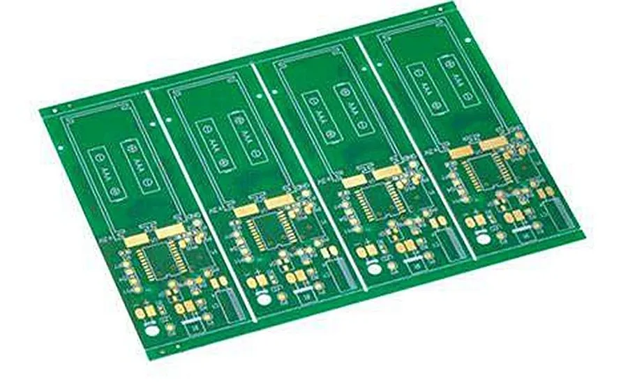
Double Sided PCB Manufacturing Process
The manufacturing of double-sided PCBs is a multi-stage process requiring precision and control to ensure the final product meets design specifications. It involves several key steps, from substrate preparation to final surface finishing, each crucial for functionality and reliability.
- Material Selection
The process begins with selecting the appropriate substrate material, typically a non-conductive material like FR-4 (Flame Retardant 4), known for its balance of cost, mechanical strength, and electrical properties. Other materials like CEM-1, CEM-3, or polyimide may be chosen based on specific application requirements. The dielectric constant and thickness of the substrate are crucial for impedance control. - Copper Cladding
A thin layer of copper is laminated onto both sides of the substrate, forming the conductive layers of the PCB. This copper cladding is typically measured in ounces per square foot, with common thicknesses being 0.5 oz, 1 oz, or 2 oz. The copper is then chemically treated to provide good adhesion for subsequent processes. - Imaging
The circuit pattern is transferred onto the copper layers using a photosensitive material called photoresist. The PCB is coated with photoresist and exposed to UV light through a photomask. The UV light hardens the exposed photoresist, while the unexposed portions remain soluble. The board is then developed, removing the unhardened photoresist and revealing the desired copper pattern. - Etching
The exposed copper is removed using a chemical etchant, leaving behind the desired copper traces and pads protected by the hardened photoresist. This process is critical to precisely define the circuit pattern. - Drilling
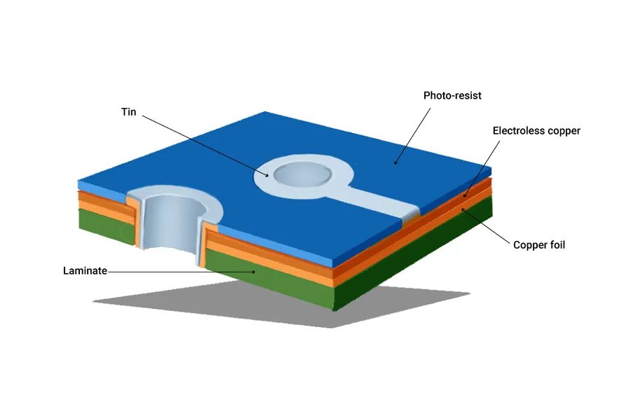
Holes are drilled through the PCB at specified locations. These holes include component mounting holes and vias. Precision drilling is essential for accurate component placement and reliable electrical connections between the two copper layers. The holes may be mechanical or laser-drilled depending on their size and precision requirements. - Plating
Following drilling, the holes are plated with a conductive material, typically copper. This plating process establishes electrical connections between the top and bottom layers and forms vias. Electroless plating initially deposits a thin layer, followed by electrolytic plating to thicken the copper layer. - Solder Mask Application
A solder mask, usually a green epoxy layer, is applied over the entire PCB, except for the pads where components will be soldered. This mask prevents solder from bridging between traces, ensures that solder stays only on the solder pads and protects the copper from oxidation and corrosion. - Surface Finishing
A final surface finish is applied to the exposed copper pads to protect them from oxidation and ensure good solderability. Common surface finishes include HASL (Hot Air Solder Leveling), ENIG (Electroless Nickel Immersion Gold), and OSP (Organic Solderability Preservative). The choice of surface finish depends on factors such as cost, performance requirements, and environmental conditions. - Silkscreen Printing
A silkscreen is often printed on the PCB to provide labels, component outlines, and other information for assembly and testing. The silkscreen is typically applied using an ink and a screen printer. - Final Inspection and Testing
The manufactured PCBs undergo final inspection and testing to ensure they meet design requirements. Tests include visual inspection, electrical continuity testing, and functional testing based on the customer's specific requirements. Quality control ensures that only functional boards are shipped.
Applications of Double Sided PCBs
Double-sided PCBs are integral to a wide spectrum of electronic devices across diverse industries due to their enhanced circuit density and routing flexibility compared to single-sided boards. They bridge the gap between the simplicity of single-sided PCBs and the complexity of multilayer boards, making them a cost-effective solution for many applications.
- Consumer Electronics
Double-sided PCBs are found in numerous consumer devices, including smartphones, tablets, laptops, and digital cameras. Their compact design and ability to support complex circuits make them ideal for these applications, where space is often a premium. - Industrial Equipment
Used extensively in industrial machinery, control systems, and automation equipment. The reliability and enhanced performance of double-sided PCBs are crucial for these demanding applications. - Automotive Industry
Double-sided PCBs play a critical role in automotive electronics, such as engine control units (ECUs), infotainment systems, and dashboard controls, withstanding the harsh operating conditions of vehicles. - Medical Devices
Employed in various medical devices, from diagnostic equipment to patient monitoring systems, where accuracy and reliability are paramount. The dual-layer design enables efficient routing for sensitive analog signals. - Telecommunications
Essential components in telecommunications infrastructure, including routers, switches, and network devices, handling high-speed data transmission effectively. - Aerospace and Defense
Utilized in aerospace and defense applications, such as avionics, radar systems, and communication devices, where performance and robustness are paramount. - LED Lighting
Double-sided PCBs are commonly used in LED lighting systems, enabling efficient heat dissipation and reliable connections for multiple LED components.
| Application Area | Specific Examples | Why Double Sided PCBs are Suitable |
|---|---|---|
| Consumer Electronics | Smartphones, Tablets, Laptops | Compact size, moderate circuit complexity, cost-effective solution |
| Industrial Equipment | Control Systems, Automation Equipment | Enhanced performance, reliable operation, good power handling |
| Automotive Industry | ECUs, Infotainment Systems | Durability, performance under harsh conditions, compact design |
| Medical Devices | Diagnostic Equipment, Monitoring Systems | Accuracy, reliability, supports sensitive analog circuitry |
| Telecommunications | Routers, Switches, Network Devices | High-speed data transmission, efficient signal routing |
| Aerospace and Defense | Avionics, Radar Systems | Robustness, high performance, long-term reliability |
| LED Lighting | LED Panels, Light Fixtures | Efficient heat dissipation, reliable connections for multiple components |
Double Sided PCB Assembly Techniques
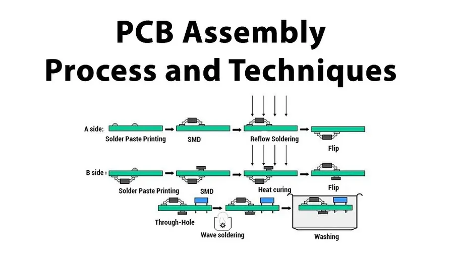
Assembling double-sided PCBs involves meticulous component placement and secure soldering techniques on both sides of the board. This process requires a thorough understanding of both surface mount (SMT) and through-hole (THT) technology, ensuring reliable electrical connections and avoiding common defects.
The assembly process requires careful considerations for component placement, soldering methods, and thermal management during soldering to ensure a robust and functional circuit.
- Component Placement
Strategic component placement is crucial for efficient soldering and circuit performance. It is crucial to consider component density, thermal constraints, and trace routing to avoid shorts and signal integrity issues. Proper orientation of polarized components is also essential for correct circuit operation. - Surface Mount Technology (SMT)
Surface mount components are soldered directly onto the surface of the PCB using automated pick-and-place machines and reflow soldering techniques. This method offers high component density and is suitable for mass production. The paste needs to be aligned precisely with the components, with careful inspection to ensure the components are not misaligned during the process. - Through-Hole Technology (THT)
Through-hole components have leads that pass through plated holes on the PCB. They are typically soldered manually or using wave soldering techniques. Although less dense than SMT, THT components provide more robust mechanical connections, especially for connectors or heavier components. Correct lead trimming is important to prevent short circuits. - Soldering Methods
Selecting the right soldering method depends on component types, production volumes, and budget. Manual soldering offers flexibility for prototyping and rework, wave soldering is suitable for THT mass production, and reflow soldering is ideal for SMT. Proper flux usage is also essential, as excessive flux can leave residue and insufficient flux can result in poor solder joints. - Reflow Soldering
Reflow soldering is the most common method for SMT, involving the use of solder paste, a precise oven temperature profile, and reflow ovens that melt and solidify the paste, forming the solder connections. Time and temperature accuracy are essential to ensure consistent solder joints, and minimize the risk of thermal damage to the PCB or components. Post-reflow inspection using visual and x-ray analysis is essential to detect any soldering defects. - Wave Soldering
Wave soldering is an efficient method for large volume through hole assembly. The PCB is passed over a wave of molten solder, connecting the component leads to the board. Process parameters including wave height, board angle and speed are carefully controlled to ensure consistent and reliable solder joints. Post-wave cleaning is essential to remove any flux residues. - Best Practices
Following best practices can improve assembly quality and reliability. This includes cleaning the board before assembly, using proper soldering techniques, and performing thorough visual and electrical testing after assembly. Consistent inspection at each stage is important for high-yield production and defect detection.
Frequently Asked Questions About Double Sided PCBs
This section addresses common questions regarding double-sided PCBs, covering their design, manufacturing, and applications. Understanding these frequently asked questions can help in making informed decisions about their use in electronic projects.
- What exactly is a double-sided PCB?
A double-sided PCB is a printed circuit board that has conductive copper layers on both the top and bottom surfaces of the substrate. These layers are connected by vias, enabling more complex and compact circuit designs compared to single-sided PCBs. This dual-layer structure allows for greater routing flexibility and component density. - How do you connect components on a double-sided PCB?
Components on a double-sided PCB are connected through a combination of surface mount technology (SMT) and through-hole technology (THT). SMT components are soldered directly onto the surface of the board, while THT components have leads that pass through plated holes and are soldered on the opposite side. Vias, which are plated through-holes, connect traces between the two layers, facilitating complex interconnections. - What are the primary differences between single-sided and double-sided PCBs?
The key difference lies in the number of conductive layers. Single-sided PCBs have a single copper layer on one side, limiting routing flexibility and circuit complexity. Double-sided PCBs have copper layers on both sides, connected by vias, enabling more intricate circuits, higher component density, and improved signal routing. This results in more compact and feature-rich designs. - What is a multi-layer PCB, and how does it differ from a double-sided PCB?
A multi-layer PCB consists of three or more conductive layers embedded within the substrate, as opposed to the two layers in a double-sided PCB. Multi-layer PCBs are used for highly complex circuits requiring a significant number of interconnections, higher signal integrity, and greater density, and are therefore more expensive. In contrast, double-sided PCBs offer a balance between complexity, cost, and performance, suitable for a wide range of electronic devices. - What are common applications of double-sided PCBs?
Double-sided PCBs are widely used in a variety of applications, including computer motherboards, power supplies, automotive electronics, industrial control systems, and various consumer electronics. Their versatility, allowing for both dense circuitry and cost-effectiveness, makes them a popular choice in numerous industries. - Are double-sided PCBs more expensive to manufacture than single-sided PCBs?
Yes, double-sided PCBs are generally more expensive to manufacture than single-sided PCBs due to the additional processing steps involved, such as plating vias and etching both sides. However, the added functionality and design flexibility often justify the increased cost, especially for more complex applications. The price difference is dependent on various factors like volume, materials and technology. - What design considerations are crucial for double-sided PCBs?
Key design considerations for double-sided PCBs include via placement to optimize routing between layers, signal integrity by minimizing impedance mismatch and crosstalk, thermal management to dissipate heat efficiently, and the physical layout to ensure component placement does not hinder assembly. Proper design techniques result in a reliable and high-performance final product.
Double sided PCBs are an essential component in modern electronics, offering superior capabilities over single-sided boards. By understanding their design, manufacturing, and assembly, you can leverage this technology for your projects. As electronics continue to evolve, mastering double sided PCB technology becomes ever more vital for achieving higher performance and greater innovation.