JLCPCB: Your Comprehensive Guide to PCB Manufacturing & Assembly
In today's fast-paced world of electronics, reliable and cost-effective PCB manufacturing is crucial. JLCPCB has emerged as a significant player, offering prototyping and assembly services to engineers and hobbyists worldwide. From complex circuit boards powering cutting-edge devices to simple boards for DIY projects, JLCPCB's impact is undeniable. This article serves as your comprehensive guide to understanding JLCPCB, its services, and how to leverage them for your next project.
Understanding JLCPCB: An Overview
JLCPCB has rapidly become a prominent player in the global PCB (Printed Circuit Board) manufacturing industry, providing cost-effective and efficient solutions for prototyping and production. Established in 2006, the company has focused on leveraging technology to streamline PCB fabrication and assembly, appealing to a diverse clientele from hobbyists to large-scale enterprises. Their commitment to high quality and rapid turnaround times has cemented their position as a leading PCB provider.
JLCPCB's core mission revolves around offering accessibility to advanced PCB technologies. They aim to reduce the barriers to entry for individuals and organizations seeking custom circuit boards, while also maintaining stringent quality standards. The company's global reach extends across numerous countries, serving a wide array of customers ranging from individual electronics enthusiasts and academic institutions to industrial companies requiring printed circuit boards for their commercial products. This wide customer base reflects JLCPCB's versatile approach to PCB production.
JLCPCB's Core Services: PCB Prototyping & Fabrication
JLCPCB excels in providing rapid and reliable PCB prototyping and fabrication services, catering to a wide spectrum of needs from simple single-layer boards to complex multi-layer designs. Their core strength lies in balancing affordability with high-quality manufacturing, making them a popular choice for both hobbyists and professional engineers.
| Feature | Details | Typical Specification | Options Available |
|---|---|---|---|
| Layer Count | Number of conductive layers in the PCB. | 1 to 4 layers standard | 1-20 layers or more available |
| Material Choices | Base material used to construct PCB | FR-4 standard | Aluminum, Rogers, Flexible PCB options also available |
| PCB Thickness | Thickness of the base material used | 1.6mm standard | 0.4mm - 2.0mm and other thickness available |
| Minimum Track Width/Spacing | Smallest allowable trace width and spacing between traces | 6mil (0.1524mm) standard | 4mil (0.1016mm) possible in advanced manufacturing options |
| Surface Finish | Protective coating applied to exposed copper | HASL standard | ENIG, Immersion Tin, OSP available |
| Copper Weight | Thickness of the copper layers on the PCB | 1oz standard | 2oz copper available |
| Manufacturing Standards | Adherence to industry guidelines and best practices | IPC-A-600 Class 2 standard | Class 3 possible for special orders |
| Turnaround Time | Time taken to complete fabrication process | 24 Hours for some services | Expedited and standard manufacturing times |
- Benefits of Fast Turnaround:
JLCPCB's rapid prototyping allows for quick iteration and testing of designs, significantly reducing product development cycles. This is critical for projects with tight deadlines or when dealing with proof of concept developments. - High Quality at low cost:
JLCPCB is able to offer lower prices through economies of scale and large order quantities, without significant compromises to quality - Online platform
JLCPCB's online order system is easy to use, and allows for streamlined design uploads and ordering.
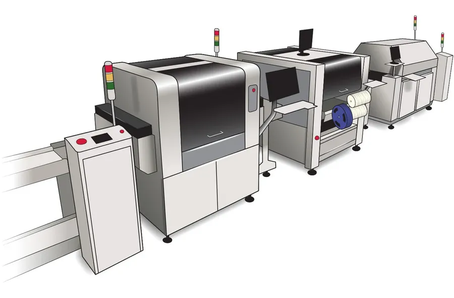
PCB Assembly Services at JLCPCB: SMT and Through-Hole
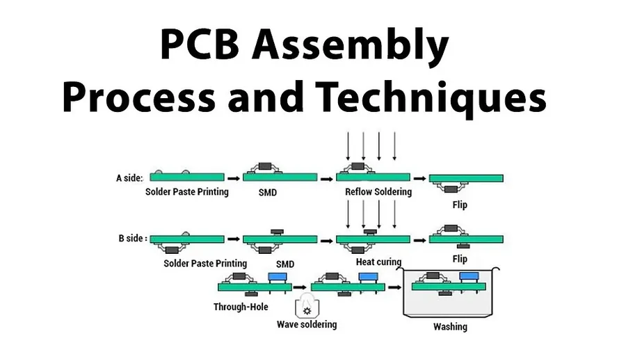
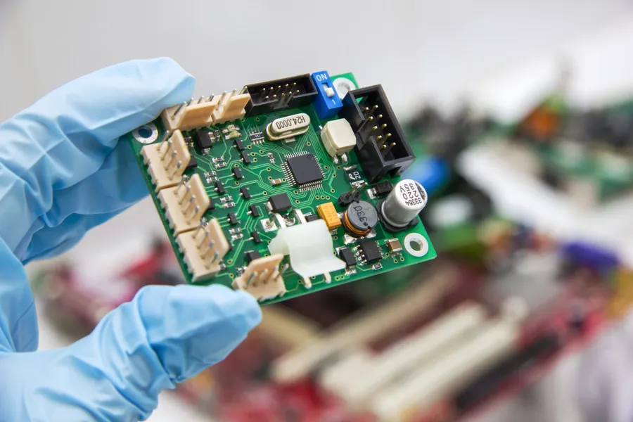
JLCPCB provides comprehensive PCB assembly services, encompassing both Surface Mount Technology (SMT) and Through-Hole assembly, catering to a wide range of electronic manufacturing needs. This service enables customers to move beyond bare board fabrication to fully assembled and functional circuit boards, streamlining the production process. By offering both SMT and through-hole capabilities, JLCPCB supports diverse project requirements, accommodating both modern, miniaturized components as well as more traditional through-hole parts.
JLCPCB's assembly service includes component sourcing, automated pick-and-place for SMT, and manual or automated assembly for through-hole components. JLCPCB maintains a stock of commonly used 'basic parts', which can simplify component selection and sourcing for many customers. For specific projects that need additional or custom components, the customer is able to source these parts and send them to JLCPCB. Proper file preparation is critical for a successful PCB assembly process, requiring both a Bill of Materials (BOM) and a Component Placement List (CPL).
| Feature | SMT Assembly | Through-Hole Assembly |
|---|---|---|
| Component Type | Surface mount components | Leaded components |
| Assembly Process | Automated pick-and-place | Manual or automated insertion |
| Component Sourcing | JLCPCB basic parts or customer supplied | JLCPCB basic parts or customer supplied |
| File Requirements | BOM and CPL files | BOM file |
To accurately prepare your files for assembly with JLCPCB, you should ensure your BOM lists every component, including the part number, manufacturer, and quantities. The CPL file is necessary for SMT assembly, providing the X and Y coordinates, rotation, and designator for each component so the automated assembly machines know how and where to place them on the PCB.
JLCPCB Pricing and Cost Analysis
Understanding JLCPCB's pricing structure is crucial for cost-effective PCB fabrication and assembly. JLCPCB offers competitive pricing, but costs vary based on several factors including order volume, PCB complexity (number of layers), and required assembly services. This section provides a detailed analysis of these cost factors to help you optimize your designs and minimize expenses.
| Factor | Description | Impact on Cost |
|---|---|---|
| Order Volume | Number of PCBs ordered in a single batch. | Higher volumes generally result in lower per-unit cost. |
| Number of Layers | The number of conductive layers in the PCB (e.g., 1, 2, 4, 6 layers). | Increased layers directly increase fabrication complexity and cost. |
| Board Dimensions | The size of the PCB. | Larger boards generally increase cost due to increased material and fabrication time. |
| PCB Material | Standard FR-4 is most common but other materials like aluminum or flex may be selected | Advanced materials command higher prices than standard FR-4 materials |
| PCB Thickness | Standard PCB thickness is 1.6mm with other options available | Non-standard thickness may affect pricing. |
| Assembly Complexity | Complexity of the assembly (e.g., number of components, SMT vs. through-hole). | More complex assemblies lead to higher costs for component placement. |
| Component Sourcing | Whether components are supplied by the user or sourced by JLCPCB (basic components vs extended parts) | Using Basic components from JLC inventory reduce component cost, Using Extended parts and user supply increase cost |
| Turnaround Time | The production speed required (standard vs expedited). | Faster turnaround times may incur additional charges. |
JLCPCB typically offers tiered pricing, with significant discounts for larger order quantities. For example, a small batch of 5 PCBs might cost more per unit than an order of 100 PCBs. Similarly, a four-layer board will cost significantly more than a two-layer board due to the added complexity in manufacturing. Understanding these tiered pricing schemes is essential for budget optimization.
For PCB assembly, the cost is influenced by the number of components, the type of components (SMT or through-hole), and whether JLCPCB sources the components or you supply them. JLCPCB offers 'basic' components in their inventory for a low cost, but for specialized parts you may need to source and supply. Using components from JLCPCB's basic parts library significantly reduces the cost of the assembly.
Here are some tips for optimizing your design to minimize cost:
- Optimize Board Layers
Use the fewest number of layers possible for your design. Start with a 2-layer board unless your circuit requires more layers. - Component Selection
Use standard, readily available components from JLCPCB's basic parts library whenever possible. Avoid unique or hard-to-source parts that may increase component sourcing costs. - Board Size Optimization
Minimize your board size, as larger boards increase cost. - Efficient Layout
Optimize your PCB layout for efficient component placement and routing, which may simplify assembly processes and reduce cost. - Avoid unnecessary features
Remove any un-needed features that can drive up costs, such as unnecessary layers, uncommon component types or materials.
How to Order PCBs from JLCPCB: A Step-by-Step Guide
Ordering PCBs from JLCPCB involves a structured process, from preparing your design files to finalizing your order. This guide will provide a practical, step-by-step approach to ensure a smooth and successful experience. The process includes preparing your design files, configuring your order on the JLCPCB website, and reviewing your Gerber files.
- Step 1: Prepare Your PCB Design Files
Export your PCB design into Gerber format. JLCPCB requires a ZIP file containing all necessary Gerber files including, but not limited to, the copper layers, solder mask, silkscreen, and drill files. Ensure that the file naming conventions are correct according to JLCPCB's documentation. It's best practice to include a readme file with a description of each of the files contained in the ZIP archive. - Step 2: Access the JLCPCB Website
Navigate to the JLCPCB website and log in or create an account. Once logged in, locate the instant quote page to begin your order. This is usually clearly marked on the home page. Start with a PCB quote page before proceeding to other services. - Step 3: Configure Your PCB Specifications
On the quote page, input all the required parameters for your PCB, including dimensions, layer count, PCB material (e.g., FR-4), thickness, surface finish (e.g., HASL, ENIG), and quantity. It's important to specify the correct dimensions of your PCB, or your quote will not be accurate. Ensure the quantity you select is the correct quantity you need. - Step 4: Upload Your Gerber Files
Upload the ZIP archive containing your Gerber files. The JLCPCB system will automatically analyze your files. Verify that the preview matches your design. Carefully review each layer in the preview, and make sure there are no obvious errors. - Step 5: Select Assembly Options (If Required)
If you also need PCB assembly, specify your SMT assembly requirements, including component placement (CPL) file, bill of materials (BOM) and quantity. Double check that the parts selected are all correct, before submitting your order. - Step 6: Review and Confirm Your Order
Carefully review your order summary, including costs and lead time. Double check all the parameters are correct, as it is very difficult to change these parameters once the order has been submitted. After confirming your order proceed with payment. - Step 7: Place Your Order and Track Progress
Once your payment is processed, JLCPCB will begin fabrication and/or assembly of your boards. You will be able to track your order progress through the JLCPCB website.
Key aspects to check when reviewing your Gerber files include ensuring that all the design layers are present, drill holes are correctly positioned, and the overall dimensions and board shape are accurate. Pay close attention to the clearance between traces and pads. It is crucial that all the design rules of your design are adhered to, as any violations will lead to failure of the PCB.
JLCPCB vs. The Competition: Advantages and Disadvantages
Choosing the right PCB manufacturer is critical for any electronics project, and JLCPCB often stands out as a strong contender. However, a comprehensive assessment necessitates comparing it against its competitors, such as PCBWay. This section provides a structured comparison of JLCPCB with other manufacturers, focusing on key factors like pricing, lead times, capabilities, and customer support, to help you make an informed decision.
| Feature | JLCPCB | PCBWay |
|---|---|---|
| Pricing | Generally lower for prototyping and small batches; tiered pricing available. | Competitive but may be higher for small quantities; varied pricing options. |
| Lead Times | Typically offers quick turnaround times, especially for standard PCBs. | Similar lead times, with expedited options available. |
| PCB Capabilities | Offers a wide range of options, including multi-layer boards, various materials, and advanced features, but can be limiting on complex designs. | Provides a broader range of material options, including advanced materials. More tolerance on complex designs. |
| Assembly Capabilities | Strong in SMT assembly, with a good selection of basic parts readily available; can source custom components. | Comprehensive assembly options including through-hole and advanced component sourcing. |
| Customer Support | Generally responsive and helpful; online support and ticketing system. | Strong customer support with dedicated account managers and faster response times. |
| Component Sourcing | Good selection of basic parts, but specialized components may require external sourcing. | More extensive component sourcing capabilities, including hard-to-find components. |
| Minimum Order Quantity | Low minimum order quantity, beneficial for small projects and prototyping. | Varies with service, can be higher than JLCPCB. |
| Shipping | Good shipping options, with tracking and express options available. | Reliable shipping options, with varied international delivery times. |
| Ease of Use | Straightforward ordering process, user-friendly interface. | Slightly more complex ordering process for beginners. |
Frequently Asked Questions About JLCPCB
This section addresses common queries about JLCPCB, providing clear and concise answers to help users understand the company, its operations, and the services it provides. We've incorporated common 'People Also Ask' questions to offer a comprehensive overview.
- Is JLCPCB a Chinese company?
Yes, JLCPCB is a Chinese company headquartered in Shenzhen, China. It operates as a global PCB manufacturing and assembly service provider, serving a diverse international customer base. - What services does JLCPCB offer?
JLCPCB specializes in PCB (Printed Circuit Board) manufacturing and assembly services. This includes PCB prototyping, fabrication, SMT (Surface Mount Technology) assembly, and through-hole assembly. They provide a complete solution from design to finished boards. - Where is JLCPCB based?
JLCPCB is based in Shenzhen, China, which is a major hub for electronics manufacturing. Their manufacturing facilities and headquarters are located there, enabling them to efficiently produce and ship PCBs globally. - How big is JLCPCB?
JLCPCB is a large-scale PCB manufacturer with a significant presence in the global market. While specific employee numbers and exact production capacities vary, they are considered a major player in the PCB industry, serving a vast customer base worldwide. They have multiple factories with large production capacity, allowing them to process high volumes of orders daily. - Does JLCPCB offer a component sourcing service?
Yes, JLCPCB offers a component sourcing service for assembly orders. They have a catalog of 'basic parts' which they can source and assemble directly. For parts outside this catalog, you typically need to source and provide them yourself, but they offer a purchasing service as well. - What is the typical turnaround time for PCB fabrication at JLCPCB?
JLCPCB is known for its rapid turnaround times, especially for standard PCB orders. Fabrication can often be completed in as little as 24 hours for some basic orders. Assembly times vary based on complexity and part sourcing but are generally quite efficient. Specific lead times depend on the complexity of the design, the number of layers, and any special requirements. It's recommended to check the current estimated lead time on the JLCPCB website during the order process. - What are the common file formats used by JLCPCB?
JLCPCB primarily uses Gerber files for PCB fabrication. For assembly, they require a Bill of Materials (BOM) file and a Component Placement List (CPL) file. These files specify the components needed and their exact placement on the PCB. They also support other file formats, such as KiCAD and Eagle project files. Always refer to their website for the latest file format requirements.
Tips and Best Practices for Designing PCBs for JLCPCB
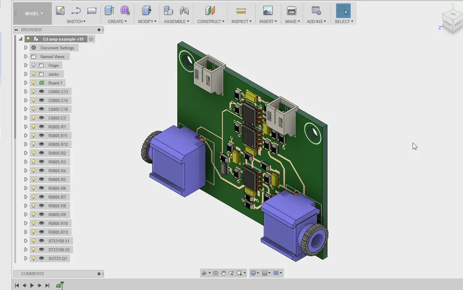
Optimizing PCB designs for JLCPCB's manufacturing process is crucial for ensuring successful production, minimizing errors, and reducing costs. Adhering to their specific design rules and capabilities is essential for a smooth transition from design to fabrication and assembly. This section outlines best practices and actionable insights to help you create PCBs that are perfectly suited for JLCPCB.
- Design Rule Checks (DRCs)
Always run thorough DRCs in your PCB design software, using JLCPCB's specific rules. These rules encompass minimum trace widths, spacing, via sizes, and annular rings. Failing to adhere to these specifications can lead to manufacturing issues. - Component Footprints
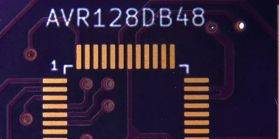
Ensure your component footprints are accurate and match the components you intend to use. Errors in footprints can lead to assembly problems. Utilize libraries that provide validated footprints, and double-check all dimensions against datasheets. For example, using the right pad size for each component is important for the best solder joints. - Gerber File Generation
Verify the correct layers are exported in your Gerber files, including copper layers, solder mask, silkscreen, and drill files. Ensure the filenames and file extensions are standard (.GTL, .GBL, .GTO, .GBO, .GTS, .GBS, .TXT). Use a Gerber viewer to confirm everything is correct before uploading, such as the accuracy of the outline, solder mask, and drill files. Using a viewer can help detect any errors, such as missing layers. - Solder Mask and Silkscreen Considerations
The solder mask and silkscreen layers should be designed with appropriate clearances and avoid overlapping with pads or vias. Ensure the silkscreen is readable and does not obscure important information. Avoid placing silkscreen over pads, which can lead to assembly issues. Maintain a minimum clearance between the soldermask and pads. - Panelization
If you are ordering multiple copies of your PCB, consider panelizing your design. Doing so will reduce per-unit costs. Consult JLCPCB's panelization guidelines to optimize the panel size and spacing for efficient manufacturing. This will help avoid any manufacturing or yield problems. - Assembly Considerations
When designing for assembly, place components such that they can be easily assembled by machine. Keep components away from the board edges. Also, make sure the orientation of components is consistent and well-documented in the Bill of Materials (BOM) and CPL files. All reference designators, particularly for SMT parts, need to be clearly marked on the silkscreen to prevent assembly errors. - Square Cutouts
Be aware that JLCPCB has limitations with square cutouts, particularly those with sharp corners. When possible, avoid them, or use rounded corners to facilitate the cutting process and prevent damage. Consider using a milling process for complex shapes that are not simple cutouts. - BOM and CPL files
When ordering assembled PCBs, ensure that your BOM (Bill of Materials) and CPL (Component Placement List) files are accurate and complete. Double-check the part numbers, quantities, and component locations before submitting them. Inaccuracies or inconsistencies in these files can result in assembly errors and delays.
JLCPCB and the Future of PCB Manufacturing
The PCB manufacturing industry is undergoing a rapid transformation, driven by technological advancements and evolving market demands. Companies like JLCPCB are not just participants but active drivers of innovation, shaping the future of how PCBs are designed, manufactured, and utilized across various sectors. This section explores these potential future trends and the impact on the industry.
Key trends and innovations that are likely to shape the future of PCB manufacturing, especially with companies like JLCPCB in the forefront, include:
- Increasing Complexity and Miniaturization
As electronic devices become smaller and more powerful, the demand for more complex, high-density interconnect (HDI) PCBs will increase. This includes finer traces, smaller vias, and tighter spacing between components. JLCPCB is expected to continue developing capabilities to produce these advanced PCBs with high precision. - Flexible and Wearable Electronics
The market for flexible PCBs and wearable electronics is growing rapidly. This includes flexible substrates that can conform to non-planar surfaces and stretchable interconnects for wearable devices. JLCPCB will likely adapt to cater to the fabrication and assembly needs of flexible PCBs as this market expands. - Integration of Advanced Materials
There's a move towards utilizing advanced materials in PCB fabrication. This could include substrates with improved thermal properties, lower dielectric constants, and enhanced mechanical strength. JLCPCB may explore these advanced materials to offer higher-performance PCBs. - Automated Manufacturing and AI
The incorporation of automation and artificial intelligence (AI) in PCB manufacturing will enhance efficiency, reduce costs, and improve production quality. JLCPCB, like other leading manufacturers, could use AI-powered systems for quality control, process optimization, and predictive maintenance. - Focus on Sustainability
Growing environmental awareness will drive a push for more sustainable PCB manufacturing processes. This includes reducing waste, using environmentally friendly materials, and optimizing resource usage. Companies will need to adapt to these demands, including companies like JLCPCB. - Enhanced Digital Design and Manufacturing
Integration of cloud platforms and digital twin technologies to allow remote design, real-time feedback and improved simulation tools, which are transforming the PCB manufacturing process, making it more efficient and agile. These will likely be supported by companies like JLCPCB to enhance customer experience.
JLCPCB's role in this evolving landscape includes leveraging its production capacity and technological prowess to adapt to these changes. Their potential evolution in key areas such as HDI, flexible PCB production, advanced material usage, and automated manufacturing processes are expected to solidify their place in the global market.
JLCPCB has revolutionized access to PCB manufacturing and assembly, making it easier than ever for engineers, hobbyists, and businesses to bring their electronic designs to life. By understanding their services, pricing, and best practices, you can effectively leverage JLCPCB for your next project. Whether you are prototyping a complex board or doing a small batch run for a personal project, JLCPCB offers a powerful and versatile solution. As the electronics landscape evolves, JLCPCB is likely to remain a key partner for many in the future. Remember to always double check your designs for optimal manufacturing when using jlc pcb.