KiCad: Your Gateway to Free and Powerful PCB Design
In today's fast-paced world of electronics, the ability to design and create custom printed circuit boards (PCBs) is increasingly vital. KiCad, a free and open-source Electronic Design Automation (EDA) suite, democratizes this capability, offering a powerful and accessible alternative to costly commercial software. Whether you're a seasoned engineer or a hobbyist tinkering at home, understanding KiCad's core functionality is crucial to bringing your electronics projects to life. This article dives deep into how KiCad can empower your designs, bridging the gap between idea and physical reality.
Understanding KiCad: Core Features and Capabilities
KiCad is a robust, open-source Electronic Design Automation (EDA) suite, providing a complete and integrated environment for designing printed circuit boards (PCBs). It encompasses all stages of the design process, from initial schematic capture to final PCB layout and 3D visualization, offering a cost-effective alternative to commercial software. KiCad empowers engineers, hobbyists, and researchers with a powerful toolkit, facilitating the creation of intricate and functional electronic devices.
| Feature | Description | Key Benefit |
|---|---|---|
| Schematic Capture | Graphical editor for creating electronic circuit diagrams. Includes tools for adding components, wiring them, and setting properties. | Accurate and clear representation of the circuit's functional logic. |
| PCB Layout Editor | Tool for designing the physical layout of the PCB. Includes footprint assignment, component placement, trace routing, and layer management. | Physical realization of the schematic, optimizing electrical performance and manufacturability. |
| Component Library | Extensive collection of pre-designed symbols and footprints. Users can also create custom components. | Reduces design time by providing ready-to-use components and enables custom part integration. |
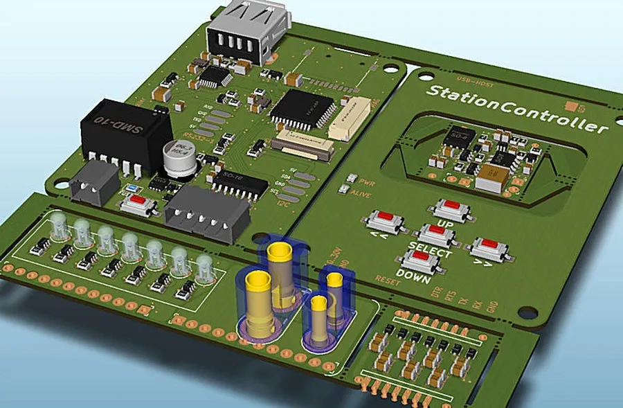
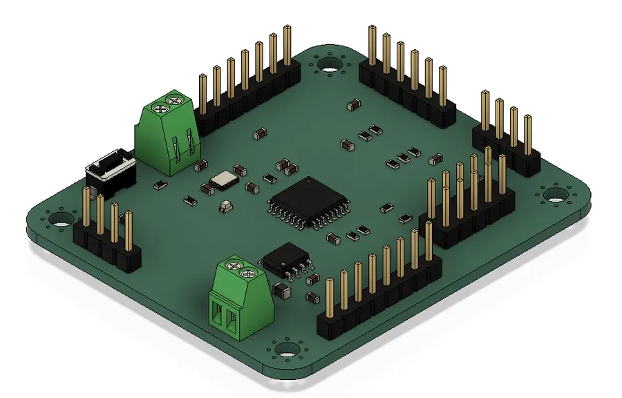
| 3D Viewer | Allows users to visualize the PCB assembly in three dimensions, including components, enclosures and mechanical fit check. | Identifies potential mechanical issues early in the design cycle and facilitates better design visualization. |
| Simulation | Integrated tools for basic simulation of circuits, allowing for analysis of design behavior. | Enhances design reliability by verifying circuit performance prior to fabrication. |
Getting Started with KiCad: Installation and Interface Overview
This section guides you through the essential steps of acquiring and setting up KiCad on your system, followed by an explanation of the user interface to familiarize you with the tools available for PCB design. The initial setup and understanding of KiCad's interface are foundational for effective use of its comprehensive features.
KiCad, being open-source software, is available for various operating systems. The process involves downloading the appropriate installer and following a straightforward installation procedure specific to your OS.
- Downloading KiCad
Visit the official KiCad website to download the latest version compatible with your operating system (Windows, macOS, or Linux). Ensure you download the full installer, not just a component. - Installation Process
Execute the downloaded installer. Follow the on-screen instructions. Default options are usually sufficient for standard installations. For Windows, ensure you have administrative rights. For Linux, using package managers is usually the easiest option. - Initial Configuration
After install, run the KiCad. The software typically opens to the main project manager window. There are minimal initial configurations to be done but you may want to set the working directory for project storage
KiCad's interface is organized into several key components which are essential for schematic design, PCB layout, and library management. Understanding the purpose of each will greatly improve efficiency.
| Panel/Tool | Description |
|---|---|
| Project Manager | Serves as the central hub for all KiCad projects. Allows creation, opening, and management of projects. |
| Schematic Editor | The primary tool for drawing and editing electrical schematics. Here you place and wire components. |
| PCB Layout Editor | Used for designing the physical layout of the printed circuit board. Allows for footprint placement, routing and layer management. |
| Symbol Editor | Used for creating and editing schematic symbols for electronic components. |
| Footprint Editor | Used for creating and editing PCB footprints that correspond to electronic components' physical dimensions. |
| 3D Viewer | Visualizes the PCB in a 3D environment, allowing for mechanical checks and design reviews. |
| Gerber Viewer | Inspect the design after the generation of gerber files before sending them for fabrication. |
KiCad's modular design means that each of these editors is typically used in sequence. The flow is generally from schematic design to PCB layout, which is then visualized and output for manufacturing.
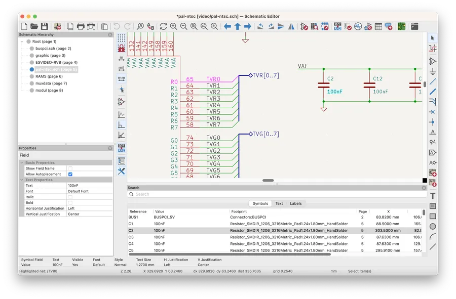
Creating Your First Schematic in KiCad
Schematic capture is the foundational step in electronic design, and KiCad provides a robust environment for creating these essential diagrams. This section will guide you through the process of building your first schematic, focusing on adding components, wiring them together, and employing best practices for clear and organized circuit representation.
- Launch the Schematic Editor
Begin by opening the KiCad project and launching the 'Eeschema' application, which is the schematic editor. - Adding Components
Use the 'Add Symbol' tool (or press 'A') to browse and select components from KiCad's extensive libraries. Place these symbols onto your schematic sheet. Start with simple components such as resistors, capacitors, and integrated circuits. - Component Placement and Annotation
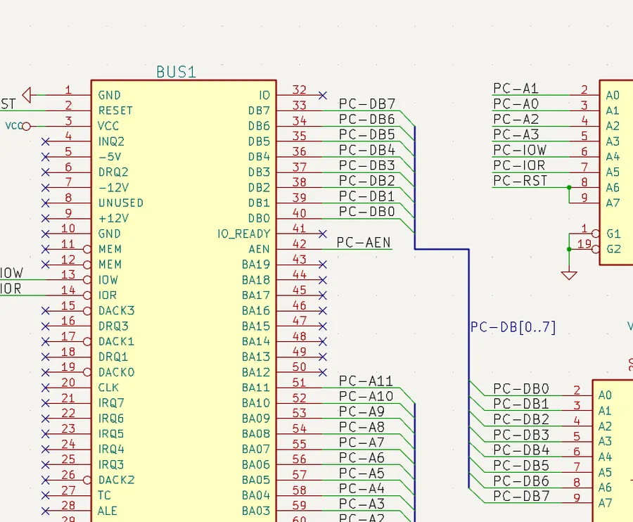
Arrange components logically on the schematic sheet for easy understanding. Annotate each component to assign a unique reference designator (e.g., R1, C2, U3) using the 'Annotate Schematic' tool. This is critical for PCB layout and bill of materials generation. - Wiring Components
Use the 'Place Wire' tool (or press 'W') to connect the component pins as dictated by your circuit design. Ensure wires accurately represent the intended electrical connections. - Adding Power and Ground Symbols
Include power (VCC) and ground (GND) symbols to establish the circuit’s reference voltage and current return paths. These symbols are critical for a functional circuit. - Using Labels and Net Names
For complex schematics, using labels to name nets (wires) can improve readability. Labels connect nets that are visually disconnected, allowing for cleaner diagrams. Use the 'Place Label' tool (or press 'L') to assign a label to any net for easy reference. - Verification and Saving
Double-check all connections and component placement. Save your work regularly to prevent loss of progress. It’s prudent to review the schematic for clarity and accuracy before moving on.
| Best Practice | Description |
|---|---|
| Component Grouping | Group related components together to reflect the circuit functionality, improving overall clarity. |
| Hierarchical Design | Use hierarchical schematics for complex projects to manage complexity by breaking the design into smaller manageable sub-circuits. |
| Clear Labeling | Label every net that provides critical signals to avoid errors when converting the schematic into a PCB. |
| Consistent Annotation | Use consistent and logical reference designator to make it easier to find the components later. |
| Regular Backups | Save your schematic frequently to prevent data loss. |
Designing a PCB Layout: From Schematic to Physical Board
The transition from a schematic diagram to a physical printed circuit board (PCB) layout is a critical stage in the electronic design process. KiCad provides robust tools for this, enabling designers to translate their logical designs into manufacturable board layouts. This involves assigning physical footprints to schematic components, strategic placement of those components on the board, routing electrical connections between components, and managing the different layers of the PCB.
This section will delve into the key steps and considerations in PCB layout using KiCad, ensuring a smooth transition from concept to physical realization. Effective PCB design requires understanding the relationship between schematic symbols and their physical counterparts, and applying design principles that optimize electrical performance and manufacturing feasibility.
- Footprint Assignment
Each component in the schematic must be associated with a physical footprint representing its actual size and pin configuration. This assignment is critical for proper component placement on the PCB. - Component Placement
Strategic component placement on the PCB is vital for signal integrity, thermal management, and manufacturability. KiCad allows interactive and automated component placement, considering component size, orientation, and electrical constraints. - Track Routing
Routing involves creating conductive paths on the PCB to connect components according to the schematic. KiCad's routing tools offer various features, including manual and automatic routing options, diff-pair routing, and via insertion. Design rules are crucial to define trace widths, clearances and ensure proper functionality. - Layer Management
Modern PCBs consist of multiple layers to accommodate complex designs. KiCad allows the management of different layers, including signal layers, power and ground planes, and silkscreen layers. This allows for the organization of different signals on the board, minimize interference and simplify the physical construction of the PCB. - Design Rule Checking
KiCad allows designers to set a comprehensive set of design rules that are checked throughout the layout process to ensure that the PCB meets the design requirements. It includes rules for trace clearance, minimum trace widths, annular ring sizes, and more. Regular design checks help to avoid potential problems during production.
| Aspect | Description | Considerations |
|---|---|---|
| Footprint Assignment | Linking schematic symbols to physical packages. | Ensure accurate pin mapping, proper package size for component. |
| Component Placement | Arrangement of components on the board. | Minimize signal path lengths, place critical components close to each other, consider thermal management. |
| Track Routing | Creating conductive paths to connect components. | Use appropriate track widths for current carrying capacity, minimize trace length, avoid sharp bends, use vias efficiently, consider impedance control |
| Layer Management | Organization of different layers in a multilayer PCB. | Use power and ground planes to reduce impedance, route high-speed signals on dedicated layers, optimize layer stackup for signal integrity. |
| Design Rule Checking | Verifying the layout against design constraints | Configure rules for trace width, clearance, via size and position, use design rules checker regularly to validate design requirements |
KiCad Library Management: Custom Components and Footprints
Efficient library management is crucial for any PCB design project. KiCad provides a robust system for managing component libraries, allowing users to create custom symbols and footprints, and leverage existing resources. This ensures design consistency, reduces errors, and streamlines the design process. Mastering library management in KiCad is essential for both beginners and advanced users to fully utilize its capabilities and maintain organized design workflows.
- Component Libraries in KiCad
KiCad organizes components into libraries, which are essentially collections of schematic symbols and their corresponding PCB footprints. These libraries are stored as files and can be easily imported and exported. KiCad comes with a substantial number of default libraries; however, many users will need to create custom libraries for specific components not found in the default set. These custom libraries can be kept locally or within a project for consistency. - Creating Custom Symbols
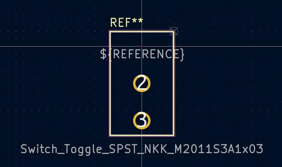
KiCad allows users to create custom symbols for schematics using the Symbol Editor. This tool enables precise design of each pin and graphic representation of the component. Important attributes such as pin names, numbers, and electrical types are defined during this process. A clear, logical, and consistent approach to symbol design is imperative for easy schematic reading and comprehension. Symbols should be named and categorized based on function, making them easy to search and reuse in multiple designs. - Creating Custom Footprints
Corresponding to every schematic symbol, KiCad requires a physical PCB footprint created using the Footprint Editor. This tool allows the designer to specify the physical pad dimensions, component outlines, silkscreen markings, and other critical manufacturing details. The precision of footprints has a direct impact on manufacturability of the PCB. Key measurements for footprints must be derived from the datasheet of the physical part or component. - Utilizing Existing Resources
Besides creating custom symbols and footprints, KiCad also allows users to expand their library with pre-made parts available online from multiple sources. Repositories like SnapEDA or component manufacturers' websites offer libraries that can be directly imported into KiCad. Additionally, collaboration and sharing of libraries within the KiCad community are quite common. This sharing of resources can further accelerate the design process. - Best Practices for Library Management
Adopting a structured approach to library management is key for the longevity and maintainability of projects. Consistent naming conventions, adequate component descriptions, and maintaining an organized directory are essential. Regularly back up libraries and versions to ensure safety against potential data loss or corruption. A standardized library structure, including clear naming conventions for symbols and footprints, is a major factor to enable design reuse, prevent accidental overwrite, and simplify collaboration with other designers.
KiCad vs. Commercial EDA Software: Advantages and Disadvantages
KiCad, as a free and open-source EDA suite, presents a compelling alternative to commercial offerings like Altium Designer and Eagle. This section provides a comparative analysis, highlighting the strengths and weaknesses of each option, focusing on cost, features, and user community, which are pivotal considerations for selecting the appropriate PCB design software.
| Feature | KiCad | Altium Designer | Eagle |
|---|---|---|---|
| Cost | Free and Open-Source | Subscription-based (High) | Subscription-based (Moderate) |
| Schematic Capture | Comprehensive | Advanced | Good |
| PCB Layout | Robust with 3D Visualization | Highly Advanced with Interactive Routing | User-Friendly but Limited |
| Component Library | Large Open Library, User Extendable | Extensive with Supplier Integration | Good, Some Restrictions |
| Simulation Capabilities | Basic Simulation Tools | Advanced Signal Integrity and Simulation | Limited Simulation Functionality |
| User Community | Large, Active and Helpful | Large Professional User Base | Large, Active Userbase |
| Customization | Highly Customizable | Moderately Customizable | Limited Customization Options |
| Learning Curve | Moderate | Steep | Moderate to Gentle |
| OS Support | Windows, macOS, Linux | Primarily Windows | Windows, macOS, Linux |
In summary, while KiCad offers a robust and cost-effective solution, Altium Designer provides advanced features for complex designs at a higher cost. Eagle occupies a middle ground, balancing usability with a reasonable price point. The choice depends heavily on project requirements, budget constraints, and user expertise.
Advanced KiCad Techniques: Simulation and 3D Visualization
KiCad extends beyond basic PCB design, incorporating powerful tools for circuit simulation and 3D visualization, enabling a comprehensive design validation process. These advanced features allow engineers to thoroughly test their designs virtually and ensure mechanical compatibility before physical prototyping, significantly reducing development time and costs.
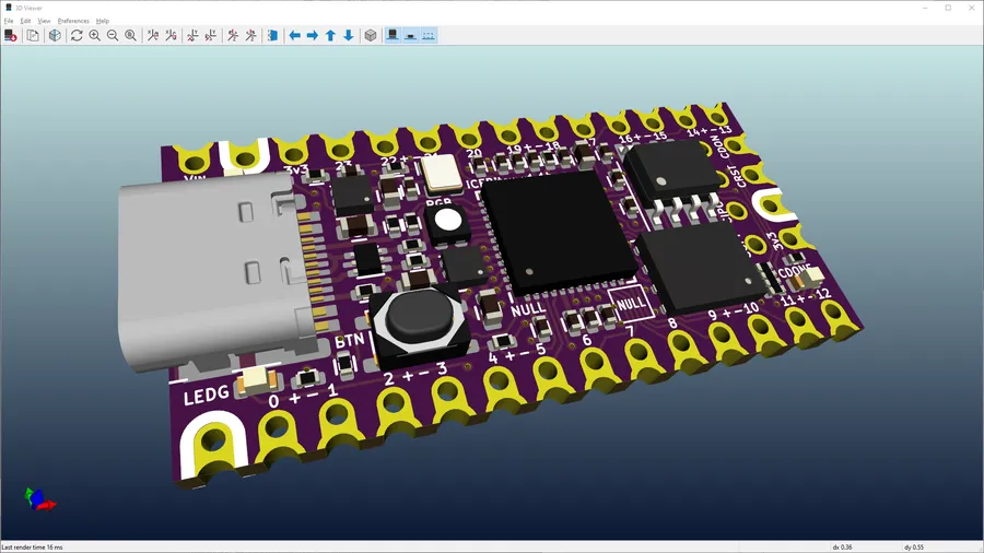
The integrated SPICE simulator in KiCad is crucial for circuit analysis, letting you verify the electrical behavior of your design. The 3D viewer provides an accurate representation of your board, allowing for mechanical fit checks and a clear understanding of the final product assembly.
- Circuit Simulation with KiCad
KiCad's integrated SPICE simulator allows for the analysis of circuit behavior. This tool provides crucial insight into how the design performs under varying conditions and parameters, including voltage, current, and frequency responses. It supports a wide range of simulation types, such as DC operating point, transient analysis, AC analysis, and more, enabling thorough design validation. - Using the 3D Viewer for Mechanical Checks
The 3D viewer in KiCad renders the designed PCB with all its components in three dimensions, allowing for detailed mechanical fit checks and pre-production validation. It enables designers to visualize the final product, ensuring that components do not interfere with each other or the enclosure, and helping identify potential issues early. The 3D viewer also allows for exporting to various 3D formats, useful for integration with mechanical CAD.
| Feature | Description | Benefits |
|---|---|---|
| SPICE Simulation | Integrated circuit simulation tool. | Verifies electrical performance, optimizes circuit parameters, avoids costly prototypes. |
| 3D Visualization | Renders the PCB in 3D. | Enables mechanical fit checks, aids enclosure design, facilitates clear understanding of the final assembly. |
Integrating both circuit simulation and 3D visualization into your workflow allows you to create a robust design verification process, reducing errors and ensuring your boards perform as expected, with the added benefit of mechanical accuracy.
KiCad Community and Resources: Getting Support and Expanding Your Knowledge
KiCad's strength lies not only in its powerful features but also in its vibrant and supportive community. This section will guide you through the various resources available to enhance your KiCad journey, from troubleshooting issues to mastering advanced techniques. Engaging with the community is key to both learning effectively and contributing to the project's growth.
- Official KiCad Website
The official KiCad website (kicad.org) is the central hub for all things KiCad. It provides access to the latest downloads, official documentation, and announcements. It's the first place to check for updates or general information. - KiCad Forums
The KiCad forums are active platforms where users ask questions, share designs, and discuss features. It's an ideal place for problem-solving and finding solutions to specific challenges. The community is very responsive, providing valuable support. - Online Tutorials and Courses
Numerous online tutorials, video courses, and blog posts are dedicated to teaching KiCad. Platforms like YouTube, Udemy, and personal blogs offer a wealth of learning materials for users of all skill levels, from beginners to advanced users. - GitHub Repository
KiCad's source code is hosted on GitHub, encouraging open contribution. Users can report bugs, request features, and even contribute code. The GitHub page also allows users to track ongoing development and understand the future roadmap for KiCad. The open-source nature of KiCad promotes transparency and community involvement in its continuous development. - KiCad Library Repositories
Beyond the official library, many community-driven repositories host custom components, footprints, and 3D models. This ensures that users have access to an extensive collection of resources when designing electronic devices. These resources are often shared on platforms such as GitHub, personal websites or community forums.
Frequently Asked Questions About KiCad
This section addresses common questions and concerns about KiCad, focusing on its cost, feature set, comparison with other EDA tools, and overall capabilities for electronic design.
- Is KiCad truly free?
Yes, KiCad is completely free and open-source software. There are no licensing fees, hidden costs, or restrictions on its use, making it accessible to everyone, from hobbyists to professional engineers. The software is distributed under the GNU General Public License. - How does KiCad compare to Eagle?
KiCad and Eagle are both popular EDA tools, but they differ significantly. KiCad is completely free and open-source with no restrictions and a robust feature set, whereas Eagle has a subscription-based model and its free version has limitations on board size and layers. Many users find KiCad as powerful as Eagle, with a different user interface and a thriving community offering extensive libraries and support. - What are the limitations of using KiCad?
While KiCad is feature-rich, some users may find its learning curve slightly steeper compared to some other EDA software. It might lack some very advanced features found in high-end commercial software like Altium Designer. However, the constant development and community contributions mean KiCad rapidly gains new features, and in most cases users will not find a limitation. - What are the advantages of KiCad compared to paid EDA software?
The primary advantage of KiCad over paid software is its cost-effectiveness; the lack of licensing fees makes it accessible to all without compromising on core functionalities. Furthermore, its open-source nature encourages community-driven improvements, resulting in a dynamically evolving tool with a wide array of support resources. The ability to fully customise the software is also a key advantage over closed-source solutions. - Is KiCad suitable for professional use?
Yes, KiCad is absolutely suitable for professional use. Many companies and engineers successfully use KiCad for complex, multi-layer PCB designs for professional applications. The capability and scope are more than sufficient for many tasks and the userbase is constantly increasing. - Can I import designs from other EDA software into KiCad?
KiCad supports importing designs from other EDA software, like Eagle and Altium in various formats. However, the level of compatibility can vary and some minor adjustments might be needed. The userbase also develops many conversion tools to assist with the import process. - Is KiCad difficult to learn?
The learning curve for KiCad is considered moderate. It might initially feel complex, but with proper learning resources, the process can be made easier. The user interface is also continuously evolving to be more intuitive, and plenty of free tutorials and online resources are available to help beginners understand the system and it's design logic.
Practical Tips for Effective PCB Design with KiCad
Effective PCB design with KiCad requires a combination of sound design principles and practical application of the software's features. This section provides actionable advice to optimize your workflow, avoid common pitfalls, and create robust and manufacturable designs.
- Component Selection and Placement
Choose components wisely based on your design requirements, cost, and availability. Begin component placement with the critical signal paths in mind, and ensure components have enough physical spacing to meet manufacturing tolerances and thermal concerns. Place decoupling capacitors close to the power pins of ICs for better signal integrity. - Schematic and Footprint Accuracy
Double-check schematic symbols and component footprints for accuracy. Ensure that all pin assignments, component dimensions, and pad shapes are correct, as errors at this stage can lead to time-consuming board re-spins. Utilize the 3D viewer to confirm that components will physically fit without interference. - Layer Management and Routing
Use KiCad's layer management effectively to separate signals, power, and ground. Route critical signal traces first, and strive for short, direct paths to reduce noise and improve signal integrity. Utilize ground planes as much as possible to provide stable references and lower impedance paths. Implement proper power distribution networks. - Design Rule Checks (DRC)
Regularly run Design Rule Checks throughout your layout process to catch violations early. Pay special attention to trace widths, clearances, via sizes, and padstack configurations, as these are common areas for issues. Customize the DRC settings to match your PCB manufacturer’s specifications to ensure manufacturability. - Annotation and Documentation
Thoroughly annotate your schematic, including part numbers, values, and any special notes. Include clear documentation, such as assembly drawings, BOM, and Gerbers, which aids both your own process and facilitates efficient manufacturing. Use net names that clearly describe the signals they carry. - Version Control
Employ version control for all your project files. This allows you to track changes, revert to previous designs if necessary, and manage collaborative efforts effectively. Git is a highly effective, highly adopted, and versatile version control system. - Iterative Design
Adopt an iterative approach to PCB design. Don't hesitate to revisit and refine your layout if necessary. Regularly seek feedback from other engineers or your manufacturers to improve the overall design and manufacturability.
KiCad is more than just a free alternative; it's a powerful and versatile EDA tool that empowers both hobbyists and professionals to design complex electronic circuits. By mastering its core features and exploring its advanced capabilities, you can bring your innovative ideas to life with ease. As the KiCad community continues to grow and evolve, expect even greater enhancements and more user-friendly workflows. Whether you're building your first project or are a seasoned engineer, KiCad is a valuable addition to your design toolkit.