Mastering Etched PCB: A Comprehensive Guide to Design, Process, and Beyond
In our technologically driven world, the humble Printed Circuit Board (PCB) plays a pivotal role in nearly every electronic device. The etched PCB, the result of carefully removing unwanted copper, is the core of many of these systems. This article delves into the intricate world of etched PCBs, exploring the various methods, materials, and considerations that go into creating these vital components, bridging the gap between the complex design and the functional electronics we use daily.
Understanding the Fundamentals of Etched PCBs
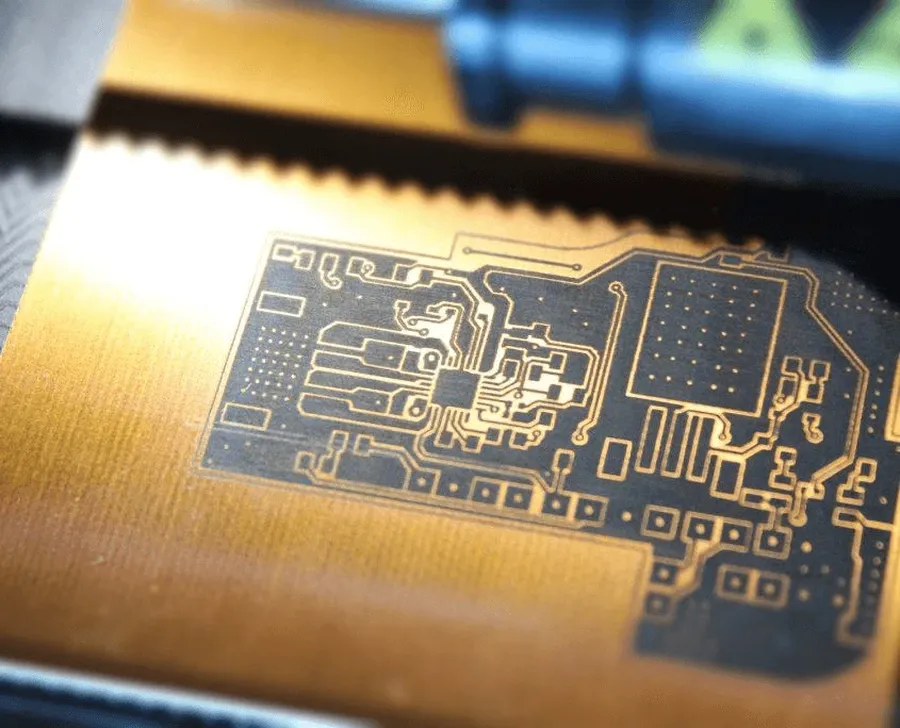
Etched Printed Circuit Boards (PCBs) are the foundational building blocks of modern electronics, providing the necessary conductive pathways for electronic components to communicate and function. The etching process, at its core, is a subtractive manufacturing technique that selectively removes copper from a copper-clad laminate, leaving behind the desired circuit traces. This process is critical for creating the intricate circuit patterns needed in nearly all electronic devices.
The primary purpose of an etched PCB is to provide a stable, reliable, and organized platform for mounting and interconnecting electronic components. The role of the etching process in this is to precisely define the conductive tracks, pads, and other features that make up the circuits. The process involves several key materials including:
- Copper-Clad Laminate
A non-conductive substrate (typically fiberglass or composite material) coated with a thin layer of copper. This is the base material for PCB etching. - Etchant
A chemical solution (e.g., ferric chloride, cupric chloride) that dissolves the exposed copper, leaving behind the desired circuit patterns. This solution is critical for the etching process. - Resist Material
A protective layer (e.g., photoresist or toner) that shields the copper intended to be retained, preventing it from being dissolved by the etchant. This material defines the trace patterns on the PCB.
Understanding these fundamentals is the first step in mastering PCB fabrication, whether for professional manufacturing or hobbyist projects. The precision of the etching process is fundamental to the performance and reliability of any electronic circuit. The selection of materials, careful design and precise execution are critical.
Common PCB Etching Methods: A Detailed Comparison

Printed Circuit Board (PCB) fabrication relies heavily on etching to remove unwanted copper, leaving behind the desired conductive traces. Several methods exist, each with its own advantages and disadvantages. This section provides a detailed comparison of the most prevalent techniques: chemical etching, toner transfer, and mechanical milling.
| Method | Description | Pros | Cons | Applications |
|---|---|---|---|---|
| Chemical Etching | Uses chemical etchants (e.g., ferric chloride) to dissolve copper. Requires a mask to protect desired traces. | High precision, scalable, cost-effective for mass production, suitable for complex designs. | Involves hazardous chemicals, requires careful handling, can be time-consuming, may produce waste. | Most common method for both prototyping and mass production. |
| Toner Transfer | Uses heat to transfer a laser-printed toner pattern onto the copper-clad board, which then acts as an etch resist. | Low cost, suitable for home-based prototyping, allows for rapid iterations. | Lower precision than chemical etching, susceptible to toner imperfections, not suitable for fine-pitch designs, may require multiple attempts to achieve a successful transfer. | DIY PCB fabrication and rapid prototyping. |
| Mechanical Milling | Uses a precision milling machine to physically remove the unwanted copper, no chemicals involved. | No chemicals required, can create complex shapes and pockets, precise depth control, suitable for low-volume productions. | Higher initial cost for the equipment, slower than chemical etching for larger boards, limited to relatively simple designs, not as cost-effective for mass production. | Rapid prototyping, low volume production, specialized designs requiring precise depth control. |
Chemical Etching: Materials, Steps, and Safety
Chemical etching is a subtractive manufacturing process pivotal in PCB fabrication, employing corrosive chemicals to remove unwanted copper, thus revealing the desired circuit traces. This method, while effective, necessitates careful material selection, precise execution, and strict adherence to safety protocols.
This section delves into the crucial aspects of chemical etching, detailing the required materials, providing a comprehensive step-by-step guide, and emphasizing the essential safety precautions to ensure successful and secure PCB production.
| Material | Description | Purpose |
|---|---|---|
| Copper-clad laminate | A substrate with a thin layer of copper on one or both sides. | The base material upon which the circuit will be etched. |
| Etchant (e.g., Ferric Chloride) | A chemical solution that corrodes and removes copper. | To remove the unwanted copper areas. |
| Photoresist (Dry film or liquid) | A light-sensitive material that becomes resistant to the etchant when exposed to UV light | To create a protective layer on the copper where etching is not desired. |
| UV light source | A light source that exposes the photoresist through the design transparency. | To selectively harden the photoresist to delineate the desired circuit. |
| Developer | A solution that removes unexposed photoresist | To remove unexposed photoresist from copper, revealing the circuit pattern. |
| Neutralizing agent | A chemical solution to halt the etching process. | To stop the chemical reaction and prevent over-etching. |
| Safety gear (gloves, goggles, apron) | Protective equipment to prevent contact with chemicals. | To prevent skin or eye irritation and to ensure a safe working environment. |
- Preparation of the Copper Clad Board
Begin by thoroughly cleaning the copper surface of the PCB with isopropyl alcohol or a specialized board cleaner, ensuring it is free from dust and fingerprints. Apply the photoresist evenly across the surface, whether using a dry film or a liquid application method, following the manufacturer's specifications for optimal adhesion. - Exposure and Development
Carefully align the designed transparency containing the desired circuit pattern onto the photoresist-coated board and expose it under a UV light source for the duration specified in the photoresist's instructions. After exposure, place the board in the developer solution. This solution will dissolve the areas of the photoresist not exposed to the UV light, thereby revealing the copper surface that needs to be etched. - Chemical Etching
Prepare the etchant solution, such as ferric chloride, according to the manufacturer’s recommended concentration and temperature. Carefully immerse the developed PCB board into the etchant bath. The etching process should be monitored and stirred gently to ensure uniform etching and the removal of unwanted copper. Periodically check the board to avoid over-etching. - Neutralization and Cleaning
Once the etching process is completed, promptly remove the board from the etchant and rinse thoroughly with water. Immerse the board in a neutralizing agent to halt the etching process completely. Afterwards, thoroughly rinse the board with water again. Then use a photoresist remover to strip the remaining photoresist from the board, revealing the etched copper traces. - Inspection and Quality Check
After all cleaning steps, the PCB board is thoroughly inspected for any remaining copper residue, etching errors, or imperfections. It is important to verify that all desired traces are accurately etched, and any shorts or broken connections are addressed before continuing in the assembly process.
Safety Precautions are paramount. Always wear appropriate personal protective equipment, including gloves, safety glasses, and an apron. Work in a well-ventilated area or use a fume hood to avoid inhaling chemical fumes. Dispose of chemicals properly according to local environmental regulations.
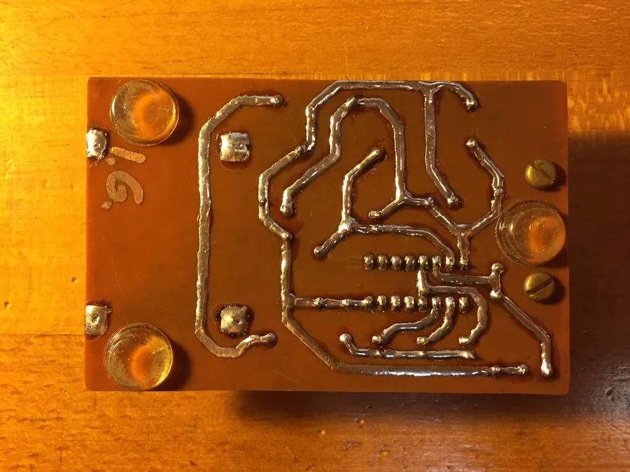
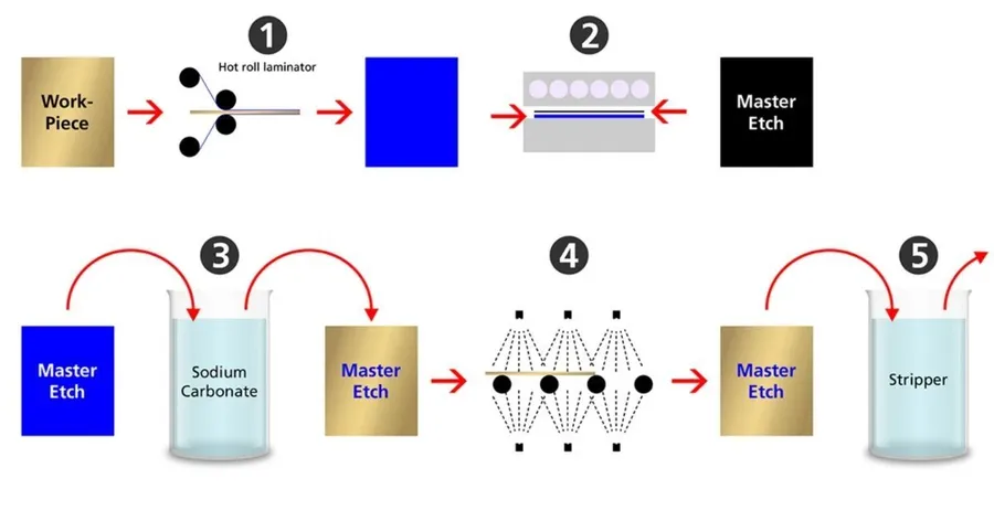
DIY PCB Etching at Home: A Step-by-Step Guide
Creating your own printed circuit boards (PCBs) at home is a rewarding endeavor, allowing for rapid prototyping and customization. This section outlines a practical, step-by-step guide for etching PCBs in a home environment, focusing on essential design considerations, material selection, and crucial troubleshooting techniques to ensure successful fabrication.
- Design Considerations
Prior to etching, design your PCB layout using suitable software (e.g., Eagle, KiCad, Altium). Ensure that trace widths and clearances match your current-carrying needs and design specifications. Export your layout as a Gerber file, then create a mask using a laser printer or similar method on a transparent film. - Necessary Materials
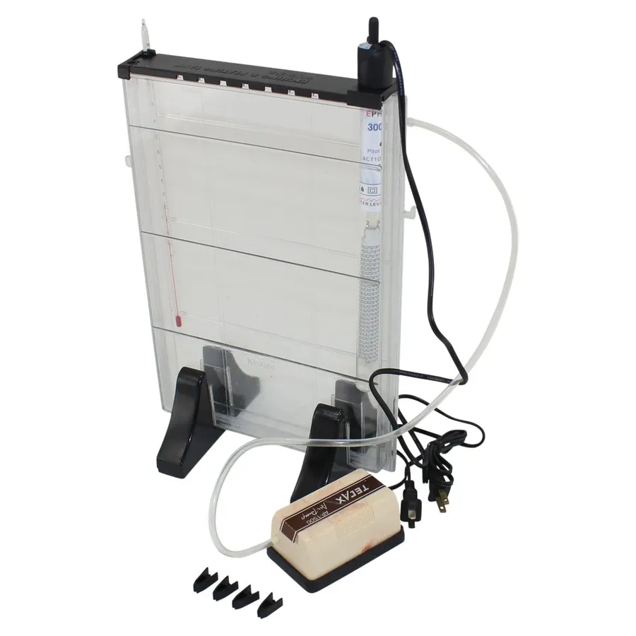
Gather essential materials: copper-clad board, laser printer, transparency film, photoresist film or paper, ferric chloride etching solution, developer solution, UV light source (optional but helpful for photoresist), etching tank or tray, protective gloves, safety goggles, and paper towels. The materials should be high quality to ensure the success of the PCB. - Step 1: Prepare the Copper Clad Board
Clean the copper clad board with a degreaser or very fine abrasive to ensure there is no oil or dirt present that may interfere with the etching process. This will allow for the photoresist film or toner to adhere correctly. - Step 2: Apply the Mask
Apply the transparent film with your layout on it to the copper clad board, using either toner transfer method by heat or UV light with photoresist film, depending on the process chosen. Ensure that the mask is adhered well to the copper, and that there are no bubbles, gaps, or other imperfections that might interfere with the etching process. - Step 3: Etching Process
Place the masked board into the ferric chloride etching solution, which is often heated for enhanced effect. Move the board around the etching tank to ensure even exposure to the etchant, and regularly check progress. The process can take between 15 and 60 minutes, based on the thickness of copper, temperature of the etchant and other factors. - Step 4: Cleaning and Inspection
Once the board has reached the required etch depth, or all the unwanted copper has been removed, rinse the board thoroughly in water, and remove the mask using a suitable solvent, or abrasive. Inspect the board carefully for imperfections and errors, and make corrections where necessary using a small file, etching marker or other suitable method. - Step 5: Post Processing
Complete the board by drilling the required holes for component insertion and through-hole mounting, if applicable. Clean the board once more, and tin plate the board as needed to prevent future corrosion, and enable better solder adhesion. - Troubleshooting Tips
Common issues include uneven etching (ensure proper agitation and consistent etchant concentration), over-etching (reduce etching time), under-etching (extend etching time), and mask failure (improve mask application). Check temperatures and concentrations of etching solutions. Check the quality of the transparency mask, or the UV exposure.
The Role of PCB Design Software and Tools
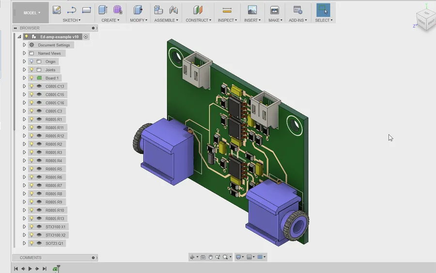
Effective PCB design software and tools are indispensable for a successful etching process, serving as the crucial bridge between conceptual designs and physical realization. These tools facilitate the layout of circuits, preparation of etching masks, and verification of design integrity prior to fabrication.
The selection of appropriate software depends on the complexity of the design and the user’s specific requirements. Each software package offers distinct functionalities, ranging from basic schematic capture and board layout to advanced simulation and analysis capabilities.
- Schematic Capture Tools
These are used to create electronic circuit diagrams, defining the connectivity of components. Key features include a library of standard symbols, netlist generation, and error checking. - PCB Layout Software
This software translates the schematic into a physical board layout. It allows designers to place components, route traces, and define board layers. - Gerber Viewers
Gerber viewers are used to inspect Gerber files generated from PCB layout software. This step ensures accurate representation of the design before etching. - Design Rule Checkers (DRC)
Integrated within layout tools, DRC functions verify designs against predefined rules for spacing, trace width, and other parameters, identifying potential fabrication issues. - Simulation Software
These tools allow designers to simulate the behavior of circuits under various conditions, providing insights into potential problems and performance characteristics before physical etching.
| Software/Tool Type | Function | Key Features | Examples |
|---|---|---|---|
| Schematic Capture | Creates circuit diagrams | Symbol library, netlist export, ERC | KiCad, Eagle, Altium Designer |
| PCB Layout | Designs the physical board layout | Component placement, trace routing, layer management | KiCad, Eagle, Altium Designer, EasyEDA |
| Gerber Viewer | Inspects Gerber files | Layer visualization, file comparison | GerbView, GC-Prevue |
| DRC | Verifies design rules | Spacing rules, trace width, clearance checks | Integrated within Layout tools |
| Simulation | Simulates circuit behavior | Spice simulation, signal integrity analysis | LTSpice, PSpice, SimScale |
Selecting appropriate design software and tools is paramount for producing accurate and reliable PCBs. These tools collectively ensure that the transition from design to physical realization is both efficient and successful, minimizing errors and maximizing the quality of the final etched PCB.
Frequently Asked Questions About Etched PCBs
This section addresses common queries related to the etched PCB manufacturing process, providing concise, authoritative answers to assist in your understanding and practical application. We draw upon established engineering principles and industry best practices to ensure accuracy and reliability.
- What is the optimal etching method for PCBs?
The 'best' etching method depends on various factors including the complexity of the design, desired precision, available equipment and budget. Chemical etching using ferric chloride or cupric chloride is a widely used, cost-effective method, suitable for many applications, while laser etching provides higher precision for complex designs, but often at a higher cost. Toner transfer methods are suitable for hobbyists and low-volume production, but may lack the precision of more advanced techniques. - How long does the PCB etching process typically take?
Etching time varies based on the etchant used, its concentration, temperature, and the desired copper thickness removal. Chemical etching can range from 15 minutes to an hour for standard copper thicknesses. Over-etching, where the copper is removed beyond the desired pattern, should be avoided, therefore, close monitoring and testing are advised. Laser etching is significantly faster and has higher throughput for large-scale production, though initial setup time may be longer. - What chemical solutions are commonly used for PCB etching?
Commonly used etchants include ferric chloride (FeCl3), cupric chloride (CuCl2), and ammonium persulfate. Ferric chloride is affordable and effective, while cupric chloride can be regenerated. The choice of etchant depends on the material of the PCB, the desired etching speed and the disposal requirements as the etchants are corrosive and considered hazardous waste. - What is the essence of etching in the context of PCB manufacturing?
Etching in PCB manufacturing is a subtractive process where specific areas of copper cladding on a PCB are selectively removed using chemicals or other methods to create the desired conductive pathways and traces. It is a crucial step in defining the electrical connections of the circuit design. The process begins with a substrate, typically fiberglass or FR4, which is coated with copper on one or both sides. A photosensitive mask is applied on this copper, and subsequently, the board is exposed to UV light to harden the mask. The unhardened mask is then removed using a developer, then the board is immersed in an etching solution, which etches away the exposed copper to reveal the final circuit pattern, thus forming the foundation of the electronic circuit. - Can I perform PCB etching at home?
Yes, DIY PCB etching is achievable at home using toner transfer methods and basic chemical etchants such as ferric chloride. However, careful attention to safety, proper ventilation, and disposal of chemicals are paramount to avoid harm or environmental damage. Consider using proper personal protection equipment like gloves and goggles. - What safety measures should be followed when etching PCBs?
When etching PCBs, wear appropriate safety gear including gloves, goggles, and protective clothing. Ensure adequate ventilation, and work in a well-ventilated area or use a fume hood if you're using chemical etchants. Always handle chemicals with extreme care and in accordance with the manufacturer's instructions, and dispose of used etchants and waste material properly according to local environmental regulations. - How does the choice of PCB material affect the etching process?
The material of the PCB substrate, primarily FR-4, influences parameters such as etch rate and minimum feature size. Different materials may also affect chemical compatibility and temperature sensitivity during etching. When using materials other than FR-4, it is important to select a compatible etchant. Material properties affect the etchant selection, ensuring successful and efficient etching.
Advanced PCB Etching Techniques and Emerging Trends
The field of PCB manufacturing is continually evolving, with advanced etching techniques and emerging trends pushing the boundaries of precision and efficiency. These innovations not only improve the quality of printed circuit boards but also open up new possibilities for electronic devices.
Laser etching and additive processes stand out as transformative technologies, impacting both the design and production of PCBs. These methods offer superior resolution and flexibility compared to traditional techniques, paving the way for complex and miniaturized electronic circuits.
| Technique | Description | Advantages | Disadvantages |
|---|---|---|---|
| Laser Etching | Uses a focused laser beam to remove unwanted copper, enabling high precision etching. | High precision, suitable for fine details, can process a wide range of materials, minimal chemical waste. | Higher initial equipment cost, may not be suitable for thick copper layers, slower than chemical etching for large volumes. |
| Additive Processes (e.g., Inkjet Printing) | Deposits conductive material onto the substrate, building up the circuit pattern. | Reduced material waste, highly flexible design options, allows for multi-layer boards with complex structures, fast prototyping. | Higher material costs, limited material compatibility, still under development for large-scale manufacturing. |
Emerging trends such as the integration of flexible substrates and the use of environmentally friendly materials further drive innovation in the PCB industry. These advancements are crucial for meeting the demands of modern electronics, which require increasingly smaller, more flexible, and more sustainable designs.
The transition towards more automated and digitally controlled etching processes is also noteworthy. These automated systems reduce human error, improve consistency, and increase production speed. As technology advances, the convergence of these trends is expected to reshape the future of etched PCBs.
Troubleshooting Common Etching Issues
Successfully etching a printed circuit board (PCB) involves navigating several potential pitfalls. Issues such as uneven etching, over-etching, and under-etching can compromise the functionality of the final product. This section provides a practical guide to identify and resolve these common challenges, ensuring a smoother and more reliable etching process.
- Uneven Etching
Uneven etching results in some areas of the copper being removed more than others. This is often due to inconsistent etchant coverage or temperature variations. To rectify, ensure the PCB is fully submerged in the etchant and that the etchant is constantly agitated to maintain a uniform temperature. A consistent and even flow across the board is essential for even etching. Also, check for any obstructions that could affect the etchant's flow. - Over-Etching
Over-etching occurs when the etchant removes more copper than intended, resulting in thinned traces or loss of fine details. This can be caused by using etchant that is too strong, excessive etching time or using an etchant solution that is already too saturated with dissolved copper. The solution is to carefully control the etching time and etchant concentration, starting with weaker solutions and closely monitoring the etching progress. Regularly replace the solution as needed. - Under-Etching
Under-etching happens when the etchant does not remove enough copper, often leaving behind unwanted copper areas and causing shorts. This is typically caused by a weak or spent etchant, insufficient etching time or poor agitation. The solution is to use a fresh or concentrated etchant solution, increase the etching time, and ensure proper agitation. Verify the etchant’s temperature and concentration according to its specifications. - Residue After Etching
Residue, or unwanted material, can be left on the board if it is not cleaned correctly. This can be prevented by using a proper cleaning method, using an appropriate solvent to dissolve any remaining photoresist, ensuring sufficient washing or post-cleaning steps are used. - Masking Issues
The mask or photoresist applied to protect the areas you don't want etched can fail. This may cause copper to etch away where it is not intended. This can be prevented by verifying good adhesion of the photoresist, ensuring a completely dry photoresist after application, following the photoresist manufacturer's instructions for proper exposure and development. - Handling and Storage of Etchant
The improper handling or storage of etchants can cause them to be ineffective, resulting in slow or uneven etching. Always store the etchant in a container made of a compatible material and in a safe environment, keep away from direct sunlight and maintain at the required temperature, follow all material safety data sheet instructions.
The etched PCB, though a small component, holds immense significance in modern technology. From basic DIY projects to complex industrial applications, understanding the process is crucial. This guide has explored the various methods of etching, from the fundamentals to advanced techniques, providing a roadmap for anyone looking to delve deeper into the world of electronics and the indispensable etched pcb, ensuring that you are now equipped to design, create, and troubleshoot effectively.