Mastering PCB Board Repair: A Comprehensive Guide

In our increasingly tech-dependent world, printed circuit boards (PCBs) are the backbone of countless devices. Understanding PCB board repairing is not just a valuable skill for electronics enthusiasts but can also extend the lifespan of many devices. This article provides a comprehensive guide to common PCB board repair techniques, tools, and best practices. We will explore diagnosing issues, performing physical repairs, and troubleshooting circuit faults to equip you with the ability to handle a wide range of repair scenarios.
Understanding PCB Board Components and Common Failure Points
A Printed Circuit Board (PCB) serves as the foundation for most electronic devices, providing both mechanical support and electrical connections for components. Understanding its components and typical failure modes is crucial for effective PCB board repairing. This section outlines these aspects, enabling more precise diagnostics and repair strategies.
Key Components of a PCB:
- Traces
These are conductive pathways, typically made of copper, that carry electrical signals across the board. They can vary in width and thickness, depending on the current they need to carry. - Pads
These are small conductive areas where electronic components are soldered to the board, providing the connection points. - Vias
These are plated holes that create electrical connections between different layers of a multi-layered PCB. They allow signals to move vertically. - Electronic Components
These include a wide range of devices such as resistors, capacitors, inductors, diodes, transistors, and integrated circuits (ICs), each serving a specific function within the circuit.
Common PCB Failure Points:
- Physical Damage
Cracks, breaks, or warps in the PCB material itself can disrupt circuit pathways. This often results from mishandling, mechanical stress, or impacts. - Component Failures
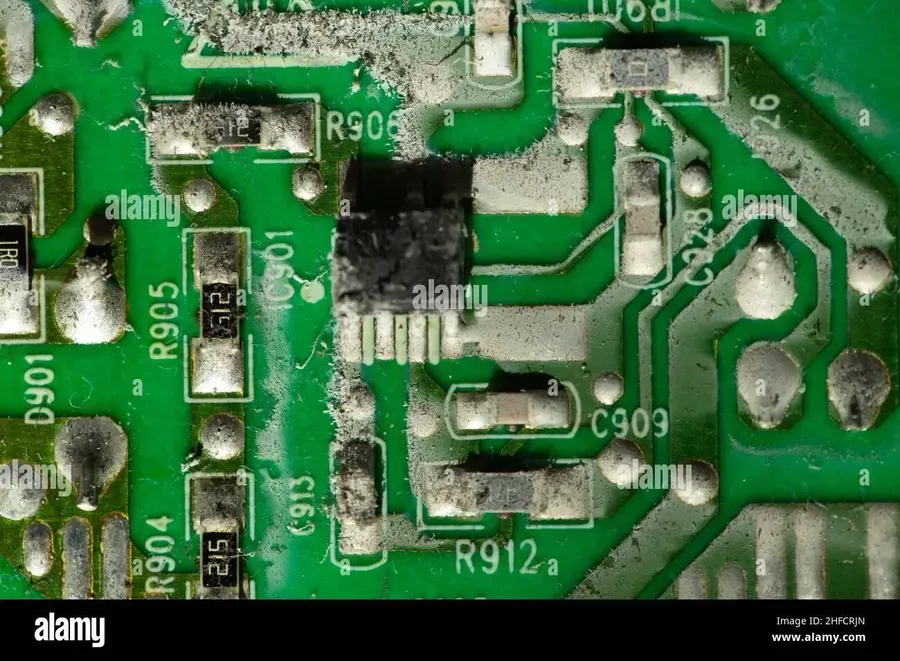
Electronic components can fail due to a variety of factors, including heat, age, overvoltage, and electrostatic discharge (ESD). These failures can manifest as open circuits, shorts, or performance degradation. - Trace Corrosion or Damage
Exposure to moisture, corrosive substances, or physical abrasion can damage the copper traces. This can lead to increased resistance or complete circuit breaks, making PCB board repairing a necessity. - Solder Joint Problems
Poor solder joints (cold solder joints) or cracked solder joints can cause intermittent connections or complete circuit failures. The quality of soldering is crucial for reliability. - Via Failures
Vias can fail due to mechanical stress or poor manufacturing, leading to layer connection issues and circuit disruption.
Essential Tools and Equipment for PCB Repair

Effective PCB board repair hinges on having the right tools and equipment. This section details the essential items needed for diagnosing and repairing PCB issues, emphasizing their specific functions and usage in the repair process. Mastery of these tools is crucial for successful PCB board repairing.
| Tool/Equipment | Function | Application in PCB Repair |
|---|---|---|
| Digital Multimeter (DMM) | Measures voltage, current, resistance, and continuity | Verifying power supply integrity, identifying shorts, testing component values |
| Oscilloscope | Displays electrical signals over time | Analyzing signal integrity, diagnosing timing issues, and identifying intermittent faults |
| Soldering Iron | Heats solder for joining or removing electronic components | Attaching and replacing through-hole and some surface-mount components |
| Rework Station | Controlled heat and airflow for soldering and desoldering components | Removing and replacing surface mount devices (SMDs) and integrated circuits (ICs) |
| Hot Air Gun | Provides a stream of hot air for heating components | Removing SMDs, shrinking heat-shrink tubing, preheating boards. |
| Precision Tweezers | Used for handling small components | Positioning and handling components, especially SMDs, during soldering and desoldering |
| Magnifier/Microscope | Provides magnified view of PCB board | Inspecting fine details, solder joints, and identifying defects. |
| Desoldering Tools (Pump/Wick) | Removes solder from joints | Preparing a board for component removal or rework |
Diagnosing PCB Board Problems: A Step-by-Step Approach
Effective PCB board repair hinges on accurate diagnosis. This section details a systematic approach to identify issues, combining visual inspection with electrical testing using a Digital Multimeter (DMM). A methodical approach is critical to pinpoint the root cause of PCB failures before attempting any repair, ensuring efficient and targeted interventions.
- Visual Inspection
Begin with a thorough visual examination of the PCB. Look for signs of physical damage such as cracks in the board, broken or burnt components, lifted pads or traces, and any corrosion. Use magnification tools if needed for detailed inspection. - Identifying Burnt Components
Burnt components, often the result of overvoltage or current surges, can be easily identified by discoloration, bubbling, or a burnt odor. Note the location and type of damaged components as it aids in understanding the potential cause of failure. Be sure to inspect components that are near burnt components as they may have been damaged by heat. - Checking for Loose Connections
Carefully inspect all connections including solder joints, connectors, and any mounting hardware. Loose connections can manifest as intermittent failures or complete loss of functionality. Gently manipulate suspect components to see if a loose solder joint can be visually identified. - Using a Digital Multimeter (DMM)
The DMM is a fundamental tool for PCB diagnostics. It is used to measure continuity, resistance, voltage, and current. When using a DMM, it is important to select the correct scale for your measurement. A systematic approach is to begin measuring from the power source and proceed through the circuit checking various nodes. - Testing for Continuity
Continuity testing verifies whether a circuit path is intact or broken. Place the DMM probes at two points in the circuit. A beep or a low resistance reading signifies continuity. No beep, or infinite resistance, indicates a break. This is useful for checking traces, vias, and connections between components. Refer to the PCB schematic diagram when performing this test. - Checking for Shorts
A short circuit is an unintended low-resistance connection between two points in the circuit. Use the DMM's resistance mode to measure between circuit nodes that should not be connected. A reading close to zero ohms indicates a short. Common causes include solder bridges or component failure. - Measuring Voltage Drops
Voltage drops across components or traces can indicate issues with the component or excessive current draw that may cause damage to other parts of the circuit. Measure voltage between different test points using a DMM. Compare the measurements to the intended voltage specified in the design to identify areas where there are discrepancies.
Repairing Cracked or Broken PCB Traces
Repairing damaged PCB traces is a critical skill in electronics maintenance, often restoring functionality without requiring full board replacement. This section outlines practical methods for addressing cracked or broken traces, focusing on effective techniques to re-establish electrical continuity and ensure long-term reliability.
Before starting any repair, careful inspection is paramount. Use a magnifying glass or microscope to assess the extent of the damage. Ensure the area is clean using isopropyl alcohol and a soft brush.
- Conductive Pens:
Ideal for minor breaks or scratches on a PCB trace, these pens contain conductive ink that bridges the gap. Ensure the ink fully connects both ends of the break and allow it to dry completely before testing. - Copper Tape:
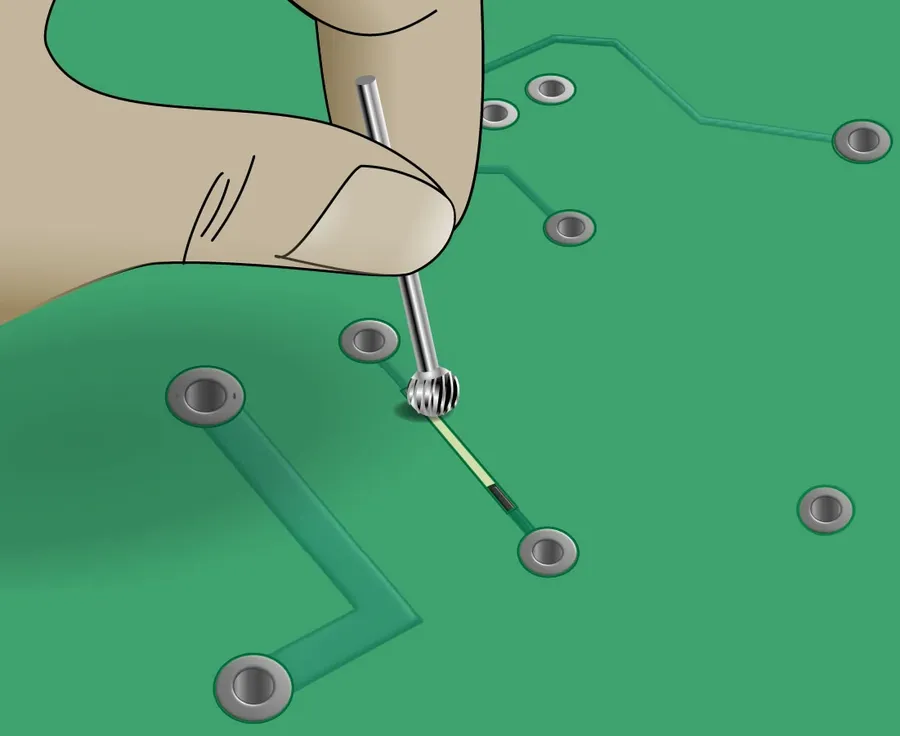
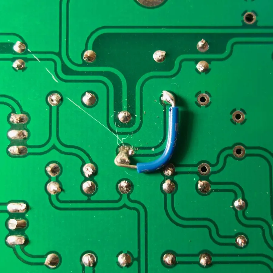
For more substantial trace damage, thin copper tape can be used. Apply the tape over the broken trace, ensuring the tape adheres well to the existing trace on both sides of the break. Use a burnishing tool or similar to ensure a good connection. The tape can be soldered to the existing trace for a stronger connection if appropriate. - Fine Wires:
When traces are severely broken or missing, fine enamel-coated wires can be soldered between the exposed ends of the trace. The wire should match the trace's gauge as closely as possible to ensure proper current flow. Solder carefully to avoid damaging surrounding components and maintain appropriate spacing between the new wire and other conductive elements.
| Repair Method | Best Use Cases | Advantages | Disadvantages |
|---|---|---|---|
| Conductive Pen | Minor breaks, scratches | Easy to apply, cost-effective | Limited durability, less reliable for high current paths. |
| Copper Tape | Larger breaks, wider traces | Good electrical conductivity, provides reasonable strength. | Can be more difficult to apply neatly, may not adhere well to all surfaces |
| Fine Wire | Severe breaks, missing traces | Strongest repair, versatile for different types of damage | Requires precise soldering, more labor-intensive. |
After the repair, verify electrical continuity using a digital multimeter in continuity mode. The resistance across the repaired area should be close to zero ohms. Test the board's functionality to ensure the repair is effective. Apply a suitable coating, such as conformal coating or epoxy, for added protection against moisture and corrosion. Careful attention to detail and thorough testing is important to ensure a reliable outcome during PCB board repair.
Replacing Damaged or Faulty PCB Components
Replacing damaged or faulty components on a PCB is a crucial skill in PCB board repair. This involves safely removing the defective part and installing a functional replacement, ensuring the board's electrical continuity and operational integrity are restored. This section provides guidance on the techniques required for both surface mount devices (SMD) and through-hole components.
The successful replacement of PCB components requires careful execution, with a particular emphasis on preventing collateral damage to the board or the new component. Proper technique and the right tools are paramount.
| Component Type | Desoldering Method | Soldering Method | Considerations |
|---|---|---|---|
| Through-Hole Components | Desoldering pump or wick | Standard soldering iron | Ensure leads are flush with the PCB; avoid overheating the component or pad |
| Surface Mount Devices (SMD) | Hot air rework station or desoldering tweezers | Hot air rework station or fine-tipped soldering iron | Use flux to ensure good solder joints, preheat board, avoid lifting pads, use a magnifier to inspect joints. |
- Component Preparation
Before removal, note the component's orientation and polarity (if applicable) using marking on the PCB or by taking a photo. Ensure that you have the correct replacement component at hand. - Desoldering Techniques
For through-hole components, use a desoldering pump or wick to remove the existing solder. For SMDs, use hot air rework stations or specialized desoldering tweezers to carefully lift the component while avoiding damage to surrounding areas. - Board Preparation
Clean the desoldered area with isopropyl alcohol to remove any residual flux or solder. Ensure that the pads are free of debris. - Soldering Techniques
Apply a small amount of flux to the pads before soldering. Use a soldering iron to heat the pad and lead, applying solder to form a solid joint. Ensure that all connections are secure and properly aligned with the pads. Use appropriate temperature and heating time to avoid overheating. - Post-Soldering Inspection
After soldering, carefully inspect all joints using a magnifier to ensure a secure and clean connection. Check for shorts or loose connections and use a multimeter to verify continuity of the circuit. Clean off remaining flux residue with isopropyl alcohol. - Safety Precautions
Always use proper safety equipment, including safety glasses and fume extraction. Handle components gently and avoid static discharge when working with sensitive electronic parts.
Repairing PCB Pads and Vias
Repairing damaged pads and vias is crucial for restoring electrical continuity and structural integrity to a PCB. Pads, the metallic surfaces where components are soldered, and vias, the plated-through holes connecting different layers of the PCB, are susceptible to damage from mechanical stress, overheating, or improper handling during component removal or installation. Effective repair ensures that components are securely connected, and signal paths are correctly maintained.
| Issue | Description | Repair Techniques |
|---|---|---|
| Lifted Pad | Pad is detached from the PCB surface, often due to excessive force or heat. | Adhesive pad repair kits, fine wires, conductive epoxy, or copper foil. |
| Damaged Via | Via is broken or has lost its plating, interrupting layer-to-layer connection. | Via repair kits (eyelets, conductive ink), fine wires, and specialized conductive adhesives. |
| Torn Pad | Pad is ripped or has a portion missing. | Pad reconstruction with specialized tools, conductive epoxy or copper tape. |
- Pad Repair Methods
The repair often starts with gentle cleaning of the affected area using a soft brush and isopropyl alcohol. For lifted pads, specialized adhesive repair kits can secure the pad back to the board, then solder the component to the now-secured pad. If the pad is severely damaged, carefully scrape away any remaining remnants and rebuild the pad using a copper foil or conductive epoxy. - Via Repair Methods
For broken vias, the process typically involves using a via repair kit. This kit often includes small eyelets or conductive paste. You can insert a small eyelet into the damaged via, securing a through connection, or using conductive paste to create the connection after cleaning the hole with a micro drill bit. - Tools and Materials
Essential tools for pad and via repair include a precision soldering iron with fine tips, a microscope or magnifying glass, fine tweezers, and a desoldering tool. Specialized repair materials like conductive epoxy, copper foil, adhesive pads, via repair kits, and fine gauge wires are also necessary for a successful repair.
Advanced PCB Repair Techniques: Reworking and Reballing
Advanced PCB repair techniques, particularly reworking and reballing, are crucial for addressing complex issues involving integrated circuits, especially Ball Grid Array (BGA) components. These methods extend beyond basic soldering and require specialized equipment and expertise to ensure effective and reliable repairs.
Reworking refers to the process of removing, replacing, or modifying components on a PCB. This often involves complex components like BGAs. Reballing is a specific type of rework that focuses on replacing the solder balls on BGA packages. These techniques are employed when components fail or when board modifications are needed during prototyping or upgrades.
| Technique | Description | Tools Required | Application |
|---|---|---|---|
| BGA Component Removal | Careful removal of a BGA chip from the PCB without damaging the component or the board. | Hot air rework station, vacuum pick-up tool, flux. | When a BGA component is faulty and needs replacement. |
| BGA Reballing | Replacement of solder balls on a BGA package to ensure proper connections on the PCB. | BGA reballing stencil, solder balls, flux, hot air rework station. | When a BGA chip is removed and needs to be re-attached or a new BGA chip is being used. |
| Hot Air Rework | Using hot air to reflow solder and replace surface mount components | Hot air rework station, nozzles | Replacing SMD components, particularly QFN and small ICs |
The process of BGA reballing involves the following steps: carefully removing the BGA chip using a hot air rework station, cleaning the BGA pads on the PCB and the underside of the BGA chip, applying flux, and then using a stencil and solder balls to create new solder ball arrays on the BGA package. Finally, the BGA is carefully aligned and reflowed onto the PCB.
Success in these advanced techniques relies not just on the right equipment, but also on the technician's expertise and the control over temperature profiles. Improper execution can lead to damage to components, or the PCB itself, rendering the board unusable.
Frequently Asked Questions About PCB Board Repairing
This section addresses common questions regarding PCB board repairs, providing practical insights to aid your repair endeavors. Understanding these FAQs can help in making informed decisions when faced with PCB malfunctions, offering clear guidance and supporting your repair process.
- Is PCB board repair feasible?
Yes, PCB boards can often be repaired, but the feasibility depends on the damage's extent and complexity. Minor issues like broken traces or component failures are often repairable, while severe damage such as extensive delamination may be uneconomical to fix. - What is the typical cost of PCB board repair?
The cost of repairing a PCB board varies widely, depending on the complexity of the repair, labor costs, and the price of replacement components. Simple repairs might cost a few dollars, while complex repairs, particularly those involving specialized tools or component replacements, could be significantly more expensive. It is advised to consult with a professional for an accurate estimate. - When should a PCB board be replaced rather than repaired?
Replacing a PCB board is advisable when the repair costs approach or exceed the price of a new board, or when damage is too extensive for effective repair. Factors include the age of the board, availability of spare parts, the extent of physical damage, and the overall criticality of the device using the PCB. - Can broken PCB traces be repaired?
Yes, broken PCB traces can often be repaired using techniques such as conductive pens, copper tape, or fine wires to bridge the broken circuit. Successful trace repairs require careful preparation, precise application, and securing of the repair. - What tools are essential for PCB board repair?
Essential tools for PCB board repair include a digital multimeter (DMM), soldering iron, desoldering tools, precision tweezers, a magnifier, and, for more advanced repairs, an oscilloscope and rework station. The specific tools required depend on the type and complexity of the repair. - How can I diagnose a PCB board problem effectively?
Effective PCB board diagnostics begin with a thorough visual inspection for burnt components or loose connections. A digital multimeter is used to test for continuity, shorts, and voltage drops, which helps to pinpoint the source of the problem. Systematic troubleshooting is key to accurate diagnoses. - How can I ensure the safety of PCB board repairing?
Ensure safety during PCB board repair by always handling sensitive components with care, taking measures to avoid static discharge, and working in a well-ventilated area. Use appropriate personal protective equipment and maintain a clean workspace. Following established safety practices minimizes the risk of damage or injury.
Best Practices and Safety Tips for PCB Board Repairing

Effective PCB board repair requires not only technical skill but also a strong commitment to safety and best practices. This section outlines crucial safety measures and systematic approaches to ensure successful and safe repairs, minimizing risks to both the technician and the electronic components.
- Safety Precautions
Prioritize personal safety by wearing appropriate protective gear such as safety glasses and gloves. Ensure the work area is well-ventilated to avoid inhalation of fumes from soldering or chemical use. Always disconnect the PCB from any power source before commencing repair work. Work on an ESD-safe surface with grounding and antistatic wrist straps to avoid component damage due to electrostatic discharge. - Handling Sensitive Components
Handle all electronic components with care, especially when working with sensitive devices like CMOS or integrated circuits. Avoid touching pins or contacts directly; use tweezers or other non-conductive tools. Always store sensitive components in anti-static containers or bags to prevent damage from electrostatic discharge (ESD). - Avoiding Electrostatic Discharge (ESD)
Electrostatic discharge can cause irreversible damage to sensitive electronic components. Use ESD-safe mats, wrist straps, and containers. Ensure all tools and equipment are properly grounded. Avoid wearing clothing that can generate static, and work in a controlled environment with stable humidity. - Proper Ventilation
Soldering and use of certain chemicals releases fumes that can be harmful. Ensure proper ventilation in your workspace to avoid inhaling these. Use fume extractors and work near open windows, if possible. In poorly ventilated spaces, wear a respirator or a mask designed to filter out soldering fumes. - Workspace Organization
A clean and organized workspace is essential for efficient and safe PCB repair. Keep all tools and components in their designated places. Avoid clutter to reduce the risk of accidental damage or loss of small parts. Use well-lit work surfaces to ensure clear visibility, and avoid distractions while working. - Systematic Approach
Adopt a systematic approach to PCB repair, starting with a thorough visual inspection, followed by diagnostic testing using appropriate tools like digital multimeters and oscilloscopes. Document your process. Before disassembling any device or part, note it's orientation and position to avoid mistakes during reassembly. Test the repaired sections before moving on to the next to make sure each problem is resolved and not compounded. Keep a log of your repairs so that you can refer back to your process on similar issues.
Effective PCB board repairing requires a blend of knowledge, skill, and the right tools. This guide has covered various techniques, from basic fault diagnosis to component-level repairs. By mastering these methods, you can extend the life of your electronic devices and save resources. Remember, safety is paramount, and continuous practice will refine your skills in PCB board repairing, enhancing both your efficiency and confidence. The ability to troubleshoot and repair PCBs will not only make you a savvy electronics user, but also a valuable asset in maintaining a sustainable technology ecosystem.