Mastering PCB Design with DipTrace: A Comprehensive Guide
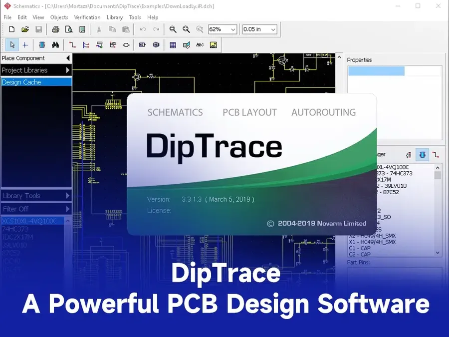
In today's world, electronic circuits are the bedrock of countless technologies. Whether it's a complex mobile phone or a simple LED circuit, these require detailed design processes. Among various tools, DipTrace stands out as a powerful yet user-friendly PCB design software. This article will guide you through the essentials of DipTrace, helping you master PCB design with ease and efficiency. We'll cover everything from fundamental concepts to advanced techniques, ensuring you have a complete understanding of how DipTrace works and how it benefits your design projects. We will also answer common questions about the software.
Understanding the DipTrace Interface
The DipTrace interface is designed for efficient PCB design, offering a streamlined workspace with key tools logically arranged. This section provides a comprehensive overview of the user interface, detailing its main components and how to customize them for optimal workflow.
- Main Toolbar
The main toolbar is located at the top of the application window and provides quick access to commonly used functions, such as creating new projects, opening existing projects, saving work, and basic editing commands. The icons are intuitive, designed for ease of use. - Menu System
The menu system, organized into logical categories like File, Edit, View, Place, etc., provides access to a comprehensive range of features. It allows for advanced settings and functionalities beyond those available on the main toolbar. Users can customize some menu options for an optimized workflow. - Workspace Layout
DipTrace offers a customizable workspace that can be tailored to individual preferences. Users can adjust window sizes, dock panels, and arrange toolbars for efficient navigation and accessibility. The workspace is split into logical areas for schematic capture and PCB layout, making it easy to shift between different design stages. - Units of Measurement
Users can specify their preferred units of measurement under the 'View' or 'Options' menu. DipTrace supports both metric (mm) and imperial (mil) units, ensuring compatibility with diverse design requirements and manufacturing standards. Proper unit settings are critical to avoid errors in the final design. - Grid Settings
The grid settings are crucial for ensuring accurate placement of components and routing of traces. Grid spacing can be adjusted as needed to match the design requirements and can be set to a specific measurement unit. Adjusting the grid will influence the snap function during schematic and layout design. These settings can be found in the 'View' or 'Options' menu.
Schematic Capture: Building Your Electronic Circuit

Schematic capture in DipTrace is the fundamental step in designing electronic circuits, where you translate your circuit ideas into a visual representation using symbols and connections. This process involves selecting components from the library, interconnecting them using wires or nets, and creating a structured blueprint of your circuit before the physical PCB layout.
- Component Placement
Selecting and placing electronic components onto the schematic canvas from DipTrace's extensive library. Components include resistors, capacitors, ICs, and connectors. - Wiring and Netting
Connecting component pins using wires (nets) to establish electrical pathways, thereby defining the circuit's connectivity. DipTrace allows for naming nets, which helps to organize large schematics. - Multi-level Hierarchy
Employing DipTrace's hierarchical design capabilities to structure complex schematics into manageable sub-circuits for clarity and reuse. This feature helps to manage large schematics with ease. - Custom Component Creation
Creating custom components by defining their symbols, footprints, and pin configurations, useful when using parts not present in the library.
During schematic creation, you'll also focus on labeling nets and components to enhance readability and assist in the PCB layout process. DipTrace supports various editing tools to ensure that the schematic diagram is clean and precise. These steps are critical for transferring the design to the PCB layout stage and should be considered a critical part of the design process. The process should be approached with a focus on clean design and clear labeling to ensure proper PCB fabrication.
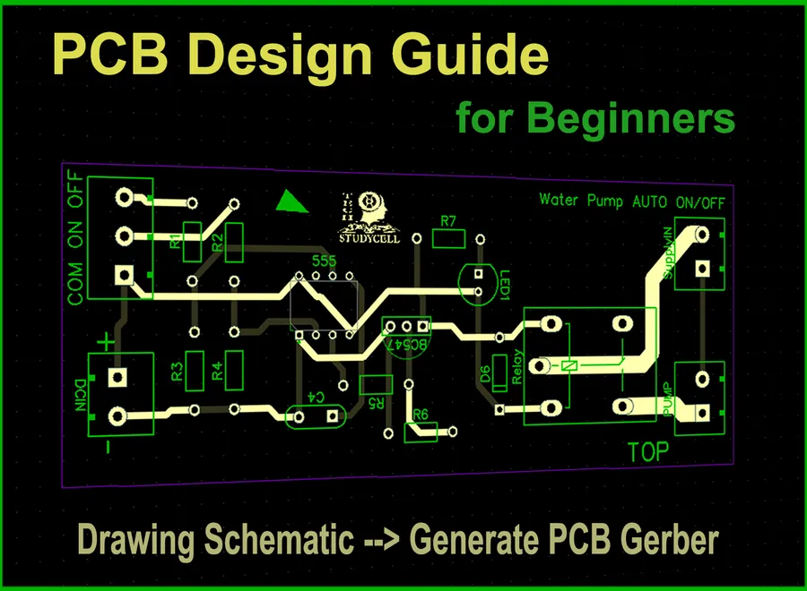
PCB Layout: Transforming Schematics to Physical Boards

The transition from a schematic diagram to a physical printed circuit board (PCB) layout is a critical step in the electronic design process. DipTrace facilitates this by providing a comprehensive set of tools that allow engineers to accurately place components, define board layers, route electrical connections, and perform thorough design rule checks (DRC) before manufacturing. The process involves importing the schematic, carefully placing components on the board, defining trace widths and spacing, and using either manual or automated routing techniques to establish the necessary electrical connections. This section will explore all the key elements of this process, from importing the schematic to completing verification prior to manufacturing, providing insight into how to use DipTrace effectively.
- Importing the Schematic
The initial step involves importing the finalized schematic design into the PCB Layout module of DipTrace. This action transfers the logical connections and component information into the physical design environment, forming the basis for PCB layout. - Component Placement
Careful component placement is essential for board functionality and manufacturability. Components should be strategically positioned to optimize routing, minimize signal interference, and ensure efficient thermal management. DipTrace provides interactive tools to assist in precise placement. - Layer Management
DipTrace allows for multilayer board designs, the number of layers is directly related to the density of components and routing complexity. Effective use of layers is critical for complex PCB design, the selection of each layer is based on the signal type and impedance requirements. - Routing Techniques
Routing is the process of creating physical pathways for electrical signals. DipTrace supports both manual and auto-routing options. Manual routing is more precise but slower, while the auto-router can provide initial trace layouts but may need manual adjustments. The choice of routing technique should be based on the circuit complexity and specific signal requirements. - Design Rule Check (DRC)
Before finalising your PCB design, it is essential to perform a Design Rule Check. DipTrace's DRC identifies violations of design parameters (trace width, spacing, etc) helping to prevent manufacturing issues and ensure the functionality and reliability of the final product. - Verification Prior to Manufacturing
Prior to sending the design for manufacturing, a final verification is crucial to ensure no errors. This includes confirming all components are correctly placed, all traces are correctly connected, and that all DRC parameters are satisfied.
| Feature | Description |
|---|---|
| Schematic Import | Transfers component and connectivity data from the schematic to PCB layout. |
| Component Placement | Tools for placing components on the PCB, with consideration of signal flow and manufacturability. |
| Layer Management | Setting up different layers for signal and ground planes in multilayer PCBs. |
| Manual Routing | Interactive placement of copper traces to connect components, providing maximum design flexibility. |
| Auto-Routing | Automatic routing of components based on connectivity rules. |
| Design Rules Check (DRC) | Verifies that the PCB design meets set standards. |
| Verification | Final verification step to catch any errors prior to sending the board for manufacturing. |
Advanced Routing Techniques in DipTrace
DipTrace provides a suite of advanced routing capabilities that extend beyond basic track placement, enabling the efficient design of complex multilayer PCBs. These techniques are crucial for high-speed digital and analog circuits, ensuring signal integrity and optimal performance. Mastery of these techniques allows for significant improvements in board layout and manufacturability.
- Differential Pair Routing
Differential pair routing is used for high-speed signals, where two traces are routed in close proximity with specific impedance control. DipTrace facilitates this with tools for precise gap control and length matching, essential for minimizing signal reflections and noise. - Bus Routing
Bus routing allows a group of parallel traces to be routed simultaneously, greatly speeding up layout for data and address lines. DipTrace’s tools for managing spacing and width consistency help in maintaining uniform electrical characteristics across the entire bus. - Via Management
Vias are used to connect traces on different layers of a multilayer board. DipTrace supports various via types, including blind and buried vias, allowing for optimized layer transitions and complex routing strategies. Careful management of via placement is crucial for signal integrity and thermal management. - Layer Transitions
Managing layer transitions efficiently is key in multilayer PCB design. DipTrace provides tools for precisely controlling via placements and ensures clear signal pathways between layers. Proper planning for these transitions minimizes signal discontinuities and maintains signal integrity. - Tear Drops
Tear drops at the connection points of traces to pads or vias reduce stress on these critical joins and improve manufacturability. DipTrace's tear drop tool allows for customizable tear drop shapes and sizes, enhancing both mechanical strength and signal reliability.
| Technique | Description | DipTrace Features | Benefits |
|---|---|---|---|
| Differential Pair Routing | Routing two traces with a specified gap to maintain impedance control. | Gap control, length matching | Minimizes signal reflection, reduces noise |
| Bus Routing | Routing parallel traces for data/address lines. | Spacing management, width consistency | Faster routing of multiple signals, consistent electrical characteristics |
| Via Management | Connecting traces between different layers. | Blind and buried vias support, precise placement | Optimized signal pathways, improved signal integrity |
| Layer Transitions | Moving signal pathways between layers efficiently. | Via placement control, clear pathways | Minimizes signal discontinuities, maintains signal integrity |
| Tear Drops | Reinforcing critical connection points. | Customizable shapes and sizes | Improved mechanical strength and signal reliability |
Library Management: Symbols, Footprints, and 3D Models in DipTrace

Efficient library management is crucial for streamlined PCB design using DipTrace. This section details how to effectively manage existing component libraries, acquire new components from online resources, create custom components, and utilize 3D models for design verification.
DipTrace's component libraries are organized into symbols (schematic representation), footprints (physical layout on the PCB), and 3D models (visual representation of the component). These three elements are linked together to facilitate the design process.
- Managing Existing Libraries
DipTrace allows users to browse, search, and organize existing libraries. Components can be viewed by category, keyword, or custom filters. Furthermore, users can create custom libraries to keep frequently used components easily accessible. - Searching and Downloading Components from Online Resources
DipTrace integrates with online component libraries like SnapEDA and SamacSys, providing access to millions of components. These resources offer direct access to pre-built symbols, footprints, and 3D models, which significantly speeds up the design process. The process is simplified, with most components offering a direct import into the user's DipTrace environment. - Creating Custom Components
When a component is not available in existing libraries, DipTrace provides tools for creating custom symbols, footprints, and 3D models. The symbol editor is used to create the schematic representation, while the footprint editor is used to design the physical layout and the 3D model editor to import and position the component for visual verification. These tools are also available for modification of any existing component in the libraries as well. The process usually involves understanding the component's datasheet to get accurate pinout and physical dimensions. This assures accurate component fit on your PCB and ensures proper connectivity in your schematic. - Using 3D Models for Visualization and Verification
DipTrace's 3D viewer is a valuable tool for visualizing how components will physically appear on the board. 3D models can be imported and positioned on the PCB design. This feature aids in collision detection, ensuring that components do not interfere with each other. This process helps to reduce potential manufacturing issues. This process also allows for proper mechanical fit verification in the design stage.
3D Preview and Export Options
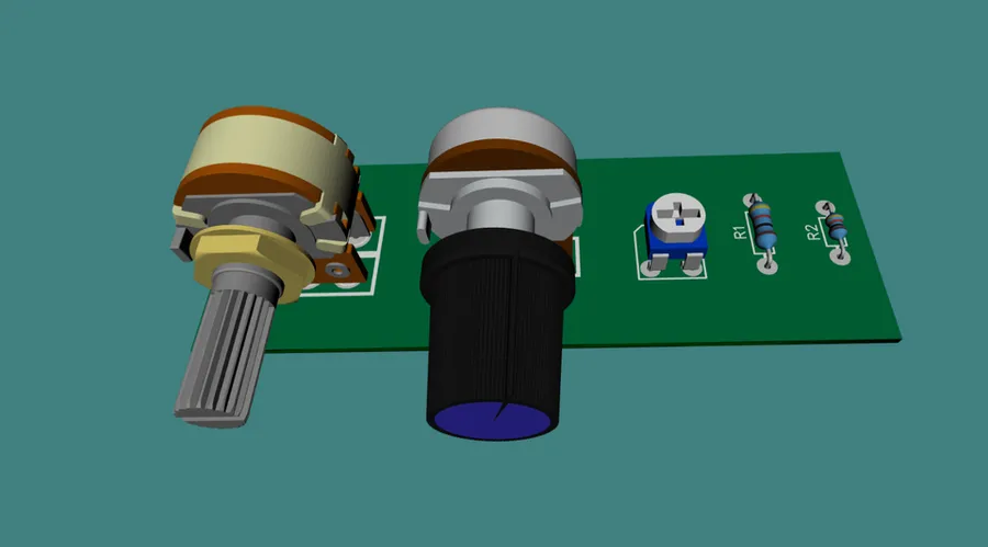
DipTrace's 3D preview capability provides an invaluable tool for visualizing your PCB design in three dimensions, facilitating collision detection and ensuring proper fit before manufacturing. Furthermore, the software supports exporting design files in multiple industry-standard formats like Gerber, ODB++, and DXF, streamlining the manufacturing process. The functionality also includes the generation of critical manufacturing files and Bill of Materials (BOM).
- 3D Preview Features:
DipTrace's 3D preview allows users to view the assembled PCB with all components, facilitating visual inspection for potential mechanical issues, component collisions, and overall design aesthetics. This preview accurately reflects the board's dimensions and component placements, ensuring designs are manufacturable before any physical prototyping. - Collision Detection:
A crucial aspect of the 3D preview is the ability to detect collisions between components or between components and the board, preventing potential assembly issues. This feature is critical for complex designs with tightly packed components, ensuring that physical assembly will proceed smoothly and that the final manufactured board will meet the design's spatial requirements. The software alerts designers to these conflicts early in the design process. - Exporting Gerber Files:
Gerber files are the standard for PCB fabrication, and DipTrace generates these files with precision, including data for copper layers, solder mask, silkscreen, and drill information. The program supports RS-274X format, which is widely accepted by PCB manufacturers. Proper generation ensures an accurate representation of your design for manufacturing. - Exporting ODB++ Files:
ODB++ is a more intelligent data exchange format, containing layer data, netlist information, and component information in one single file. DipTrace supports exporting to ODB++, which can reduce manufacturing errors and streamline communication with fabrication houses that support this format. - Exporting DXF Files:
DXF files provide a vector-based output of your board outline, useful for mechanical drawings and integrations with other CAD software. This is beneficial for mechanical engineers who need to design enclosures and other related parts, guaranteeing the PCB fits perfectly within the designated space. - Bill of Materials (BOM) Generation:
DipTrace can automatically generate a comprehensive BOM, listing all components used in the design, including their part numbers, values, manufacturer details, and quantities. The BOM is easily exported in CSV or Excel formats, which can be directly used by purchasing departments to order parts for assembly.
DipTrace Frequently Asked Questions: Addressing Common Queries
This section addresses frequently asked questions about DipTrace, a popular software for PCB design. We aim to provide clear, concise answers to help both new and experienced users understand its capabilities and how it compares to other tools.
- What is DipTrace Primarily Used For?
DipTrace is a comprehensive software suite used for electronic design automation (EDA), specifically for creating schematics and printed circuit board (PCB) layouts. It facilitates the design of electronic circuits from concept to manufacturing, including component placement, routing, and generation of manufacturing files. - How Does DipTrace Compare to KiCad?
DipTrace and KiCad are both popular PCB design software. DipTrace is often praised for its user-friendly interface and relatively short learning curve, making it suitable for beginners and smaller design teams. KiCad, being open-source, offers extensive customization options and a vast community but might have a steeper learning curve. The choice often depends on user preference, project complexity and budget considerations. - Is DipTrace a Good Choice for PCB Design?
DipTrace is considered a robust and effective PCB design tool. Its intuitive interface, combined with a full suite of features, makes it suitable for a wide range of PCB designs. However, its suitability depends on user preference and specific project needs. Features such as the 3D preview capability and robust routing tools can be very beneficial to a designer. - What Are Some Alternatives to DipTrace?
Alternatives to DipTrace include KiCad (open source, community driven), Altium Designer (high-end, feature-rich), Eagle (user-friendly, subscription-based), and OrCAD (industry standard, feature-rich). Each software has its own strengths and limitations, with the best choice depending on factors such as project complexity, budget, and user experience. - Can I Import Designs From Eagle Into DipTrace?
Yes, DipTrace supports importing designs from Eagle. This functionality allows users to migrate existing designs from Eagle to DipTrace, making it convenient for those transitioning between platforms. The process typically involves exporting the design data in a format that DipTrace can recognize (often XML-based) and importing it using DipTrace's import functions. - Is DipTrace Suitable for High-Density or Multilayer PCB Designs?
DipTrace is capable of handling complex PCB designs, including high-density and multi-layer boards. Its advanced routing features, coupled with its layer management capabilities, support complex PCB structures, including fine pitch devices, differential pairs, and controlled impedance routing, although some limitations do exist at the highest end of the spectrum compared to professional packages like Altium Designer. - Does DipTrace Offer Component Library Support?
Yes, DipTrace includes a comprehensive component library management system, allowing users to access pre-existing components, create custom components, and import from external libraries. Its integration with component data providers like SnapEDA and SamacSys can streamline the design process by automatically linking schematic symbols, PCB footprints, and 3D models.
Tips and Tricks for Efficient DipTrace Usage
Optimizing your workflow in DipTrace is crucial for efficient PCB design. This section provides actionable tips and tricks to enhance your productivity, covering aspects from software organization to automation strategies.
- Project Organization
Establish a consistent folder structure for your projects to keep related files together. Use descriptive naming conventions for schematic and PCB files to avoid confusion. This can be achieved by creating project-specific folders that contain schematic files, PCB layouts, and library components, as well as a revision history or a clear method of version control. - Customizing the User Interface
Tailor DipTrace to your design needs by configuring the toolbar, menus, and workspace layout. Customizing the toolbars to include your most commonly used commands reduces the time spent navigating through menus. In addition, use custom keyboard shortcuts for rapid access to the tools and functions used most often. - Hotkeys and Shortcuts
Leverage the hotkey system and shortcuts to significantly speed up your design process. Memorize or customize common commands. In DipTrace, using hotkeys to toggle layers, perform routing actions or quickly access commonly used commands in the component libraries is extremely efficient. - Component Libraries Management
Properly managing libraries can help streamline workflow. A well maintained and organized library, can save considerable time searching for components and ensuring consistency throughout designs. Organize components in a logical way, use clear naming conventions, and check for consistency between schematics and layouts for your components. Utilizing centralized and version-controlled libraries can also ensure data integrity. - Automation Tools
Use DipTrace automation features, such as the auto-router, and scripting features where applicable, to reduce manual effort. Automating repetitive tasks with scripts or batch processing can save considerable time when performing functions such as the generation of manufacturing files. Take advantage of features that can be used to streamline the process. - Design Rule Checks
Regularly run DRC to identify and resolve issues during layout design. Performing design rule checks (DRC) frequently during the layout process can reduce the time spent troubleshooting errors later in the process, thus helping to ensure design manufacturability and performance. Adjusting DRC rules to your design needs can also improve the efficiency of the checks. - Version Control
Use a version control system to keep track of changes to your design. This allows multiple revisions and rollbacks if needed.
DipTrace provides an effective and user-friendly solution for PCB design, suitable for both beginners and experienced engineers. With its comprehensive set of features, DipTrace enables efficient schematic capture, PCB layout, and 3D visualization. By understanding and mastering DipTrace, you can elevate your electronic projects and bring your ideas to life more efficiently. Whether you're a student, hobbyist, or professional, DipTrace is a valuable tool to have in your arsenal. It also allows you to effectively collaborate with design teams and manufacturing partners. With DipTrace you're ready to tackle any PCB project.