Mastering PCB Footprints: A Comprehensive Guide for Design Success
In the intricate world of electronics, the humble 'footprint' of a PCB is more than just a shape—it's the very foundation upon which reliable devices are built. Just as a building's foundation must be precise, so too must the footprint of electronic components on a printed circuit board (PCB). This article explores the critical aspects of PCB footprints, bridging the gap between theory and practical application to ensure your next project stands strong.
Understanding the Basics of PCB Footprints
A PCB footprint, at its core, is the physical representation of a component's connection points on a printed circuit board. It serves as the crucial intermediary for component attachment, both physically and electrically, ensuring that components are correctly placed and integrated into the circuit. Distinguishing between 'footprint' and 'land pattern' is essential, where the land pattern refers specifically to the copper pads, while the footprint encompasses the pads, silkscreen, and other related physical data.
Key Elements of a PCB Footprint

A PCB footprint is comprised of several critical elements that define how a component is physically and electrically connected to a printed circuit board. These elements ensure proper component placement, secure soldering, and reliable electrical performance. Understanding each part is crucial for accurate PCB design.
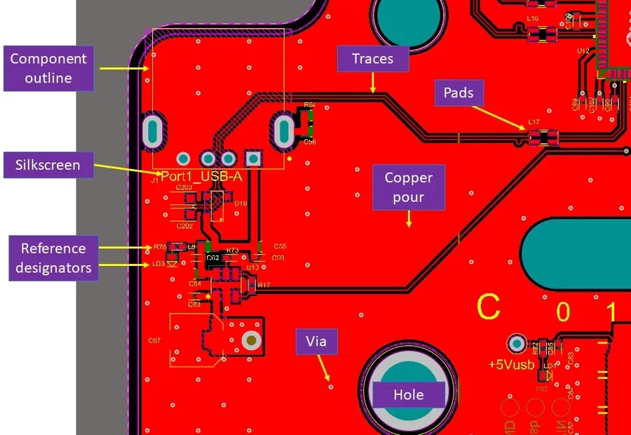
- Pads
Pads are conductive areas of copper on the PCB that form the physical connection points for component leads or terminals. There are two main types of pads: Surface Mount (SMT) pads designed for components that are soldered directly onto the surface, and Through-Hole (THT) pads with holes for inserting component leads. - Copper Layer Layout
The copper layer layout is essential for creating conductive paths that enable electrical current to flow within the footprint, ensuring a solid connection between components and the PCB traces. - Solder Mask
The solder mask is a non-conductive coating that covers most of the PCB’s surface. Openings in the solder mask, called solder mask reliefs, expose the copper pads, thus allowing solder to attach to the component leads. This process is crucial in ensuring precise soldering while protecting other areas. - Silkscreen
Silkscreen is the layer of ink applied to the PCB that provides information about the component. This includes component reference designators (e.g., R1, C2), pin 1 markers, and outlines for component bodies. It is used to guide assembly and debugging. - Mounting Holes
Mounting holes are used to secure components to the PCB using screws or other fasteners. These holes can also serve as reference points during assembly. In some cases, they may be connected to the ground layer to improve mechanical stability and electrical grounding. - Reference Pin Indicators
These indicators, usually a dot, a square, or a notch, mark pin 1 of an IC or other components with polarity, which ensures that the component is placed correctly during assembly to prevent reverse connection problems.
Importance of Accurate Footprint Design
Accurate PCB footprint design is paramount for successful electronic product development, directly influencing component placement precision, signal integrity, thermal management, and overall assembly quality. Deviations from precise footprint specifications can precipitate a cascade of issues, ranging from assembly failures to compromised electrical performance and reliability concerns.
The ripple effects of an inaccurately designed PCB footprint are far-reaching. For instance, incorrect pad dimensions or spacing can lead to component misalignment during assembly, resulting in poor solder joints, which can introduce intermittent connections or even complete circuit failures. Moreover, the precise dimensions of copper pads are crucial for signal integrity, where impedance mismatches due to poorly designed footprints can lead to signal reflections, ringing, and signal loss, particularly at high frequencies. Furthermore, thermal management can be greatly affected, especially for power components. A footprint that does not facilitate adequate heat dissipation can lead to overheating and reduced lifespan.
| Impact Area | Consequences of Inaccurate Footprints |
|---|---|
| Component Placement | Misalignment, poor solder joints, assembly failures |
| Signal Integrity | Impedance mismatches, signal reflections, noise, signal loss |
| Thermal Management | Overheating, reduced component lifespan, reliability issues |
| Assembly Quality | Difficult or impossible assembly, increased rework costs |
| Production Costs | Increased manufacturing time, lower production yield, financial losses |
Therefore, meticulously designing and verifying PCB footprints is not merely a procedural step but a foundational requirement for ensuring robust and high-performing electronic devices. Adherence to standards and meticulous design practices mitigates the risk of these negative outcomes, directly translating into cost savings, faster time to market, and enhanced product reliability.
Designing Your Own PCB Footprints
Creating custom PCB footprints is a critical skill for electronics engineers, enabling precise component integration and ensuring reliable manufacturing. This process, typically conducted within CAD software, requires careful consideration of component dimensions, tolerance levels, and adherence to industry standards, primarily those set by IPC.
The process involves multiple stages and considerations. Let's explore each step of creating a PCB footprint:
- Component Datasheet Analysis
Begin by thoroughly examining the component datasheet. This document contains vital information like component dimensions, pad locations, tolerances, and recommended land patterns. Pay close attention to the minimum and maximum dimensions as well as recommended land patterns, these values are crucial for proper pad placement and solder joint reliability. - Selecting the Correct Land Pattern
The IPC standards (such as IPC-7351) offer guidelines for land pattern design. Choose the appropriate land pattern density level (e.g., nominal, minimum, maximum) based on your design's assembly requirements and manufacturing capabilities. For example, a high density design may use minimum land patterns and a low density design may use maximum patterns. Ensure the land pattern chosen provides sufficient solderable area and reliable solder joint formation. - CAD Software Setup
Open your preferred CAD software and initiate the footprint creation process. Set the appropriate units (typically millimeters or inches) and grid spacing for precise design. You may need to configure some of the software settings to meet IPC standards, or specific company standards. Ensure these settings match the component’s datasheet specifications. - Pad Placement and Configuration
Create pads based on the land pattern chosen in step two. Ensure proper dimensions, shapes (rectangular, circular, etc.), and placement, as per the datasheet. For surface mount components, precision in pad size and position is vital for good solder joint formation. For through-hole components, ensure sufficient hole diameter for proper component insertion. Pay attention to pad clearances. There should be sufficient space to allow for good soldering, however, too much space may make the component susceptible to external stresses during operation. - Silkscreen and Solder Mask Layer Design
Add silkscreen outlines, polarity indicators, or pin one markers for easy component identification and assembly guidance. Design a solder mask that exposes the pads for soldering but covers the surrounding areas to prevent solder bridges. Ensure that the silkscreen is not placed on top of the solderable pads, and keep silkscreen markings clear and concise. - Mechanical Elements
Incorporate mechanical elements like mounting holes if they are part of the component package. Ensure the correct dimensions and placement for reliable mechanical attachment to the PCB. This should be done in the correct mechanical layer and according to the component's datasheet. - Verification and Validation
After creation, meticulously verify all aspects of the footprint. Cross-check with the datasheet values and make sure that all physical dimensions match the reference designs. It’s advisable to create a 3D model of the footprint to ensure the mechanical placement is correct. A final validation should be performed with all team members to make sure nothing was missed. - Saving and Organization
Save the newly created footprint in a central location or your company’s component library. Use clear and consistent naming conventions, making it easily searchable and manageable, and include detailed descriptions for easy future use and prevent others from re-creating a design that already exists. Make sure that the component follows your company's standards for part naming.
| Consideration | Description | Impact |
|---|---|---|
| Component Dimensions | Refer to the manufacturer's datasheet for accurate physical dimensions. | Directly affects pad placement, solderability, and component fit. |
| Tolerance Levels | Account for manufacturing tolerances to ensure reliable assembly. | Affects solder joint reliability and component placement accuracy. |
| IPC Standards | Adhere to IPC-7351 standards for land pattern design. | Ensures component compatibility, assembly success, and reduces errors. |
| CAD Software Settings | Configure units, grid, and settings to match component and design requirements. | Improves accuracy, ease of use and design quality. |
| Solder Mask Design | Design a solder mask that prevents solder bridges but ensures sufficient solderable area. | Prevents solder bridges and ensures proper soldering. |
| Silkscreen Layer | Add clear silkscreen markings for assembly and identification. | Facilitates assembly and component identification. |
Where to Find Ready-Made PCB Footprints
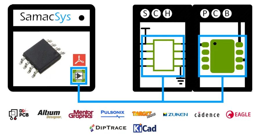
The efficient design process of printed circuit boards (PCBs) often relies on the availability of pre-existing, accurate component footprints. Instead of recreating each footprint from scratch, engineers can leverage various online resources and libraries offering a vast collection of footprints, saving considerable time and effort. However, it is crucial to verify the accuracy of any footprint before use to avoid costly errors.
- Online Component Libraries
Numerous online platforms offer extensive libraries of PCB footprints. These libraries are typically categorized by component type, manufacturer, and part number, facilitating easier searching and selection. - SnapMagic
SnapMagic (formerly SnapEDA) is a popular platform known for its vast library of component footprints, symbols, and 3D models. It aims to streamline the design process by providing designers with high-quality, ready-to-use design resources. - Samacsys
Samacsys is another well-established provider of component libraries. It provides detailed component data, including footprints and symbols, that are compatible with various CAD tools. - Manufacturer Websites
Many component manufacturers offer CAD models, including PCB footprints, directly on their websites. This is often a reliable source as the footprints are typically created by the manufacturer itself, which are more likely to be accurate. - CAD Software Libraries
Most CAD software packages come with built-in libraries of component footprints. These libraries offer a starting point for designs, but it's always wise to verify the footprint accuracy against manufacturer datasheets.
While these resources are beneficial, it is essential to note that using ready-made footprints requires careful validation against the component's datasheet to ensure dimensional and electrical accuracy. Inaccurate footprints can result in assembly issues, electrical shorts, or other performance problems.
| Resource | Footprint Quality | Cost | Ease of Use | Verification |
|---|---|---|---|---|
| SnapMagic | High | Free and Paid Options | High | Manual Check Recommended |
| Samacsys | High | Free and Paid Options | High | Manual Check Recommended |
| Manufacturer Website | High | Free | Medium | Manual Check Recommended |
| CAD Software Library | Medium | Free | High | Manual Check Mandatory |
Essential Design Guidelines for PCB Footprints
Effective PCB footprint design is critical for ensuring reliable assembly, optimal performance, and long-term durability of electronic devices. Adhering to established design guidelines minimizes common errors, enhances solderability, and guarantees component compatibility, ultimately leading to a more robust and efficient manufacturing process.
- Accurate Component Dimensions
Always use the most current datasheet from the component manufacturer to obtain the precise dimensions and tolerances. Cross-reference multiple sources if possible. Ensure the dimensions include all physical features like leads, terminals, and mounting points. - Pad Design Considerations
Pad design should adhere to IPC standards, which provide guidelines for pad size and shape. Considerations include solder fillet size, which affects solderability and inspection. The appropriate pad size is determined by component lead dimensions plus the necessary allowance for solder joint formation. - Solder Mask Clearance
A solder mask clearance should be applied around the pads to prevent solder bridging and ensure that the solder is only applied to the intended pad area. The clearance should be adjusted based on manufacturing capabilities and board density to ensure successful assembly. - Silkscreen Placement
Silkscreen should be clearly placed to help with component identification during assembly and debugging. Avoid placing silkscreen on pads or in areas that may be obstructed after the components are mounted. Silkscreen reference designators and pin 1 markers should be clearly visible. - Thermal Relief
For components connected to power or ground planes, incorporate thermal reliefs to improve solderability. Without thermal reliefs, the heat dissipation of the plane may cause issues with solder joints. The specific geometry should be adjusted according to thermal requirements and current handling needs. - Component Orientation
Pin 1 indicators or other polarity markings must be clearly defined for proper component placement during assembly. Proper orientation is critical for functionality and should be clearly visible in the footprint. Consistent orientation throughout the board will reduce error during assembly. - Footprint Verification
Before finalizing any design, always verify footprints against the component datasheet and consider test mounting the component. Ensure the physical footprint matches the expected component. A physical test will help find issues before fabrication.
Common Mistakes to Avoid When Working With PCB Footprints
Accurate PCB footprints are paramount for successful assembly and reliable operation. However, several common pitfalls can compromise the integrity of the final product. This section highlights the most frequent mistakes made during PCB footprint creation and usage, providing guidance to avoid these issues and ensure a robust design.
- Incorrect Pad Sizes
Using pads that are too small or too large can lead to poor solder joints, component misalignment, and assembly issues. Refer to the component datasheet for the recommended pad dimensions, and always take into account the manufacturing tolerances. - Missing Thermal Reliefs
For components that generate heat, it is crucial to include thermal reliefs in the pads that connect to power or ground planes. Failure to do so can cause uneven heating during soldering and thermal damage during operation. These reliefs allow heat to flow evenly to larger areas of the board. - Improper Silkscreen Placement
Silkscreen markings are essential for component identification and correct placement during assembly. Avoid overlapping pads or via holes and ensure that the silkscreen is legible after manufacturing. Misaligned or obscured silkscreen can result in assembly errors. - Inaccurate Component Orientation
Incorrect orientation of polarized components can cause circuit malfunction. Pay close attention to the component's polarity markings (such as a dot for pin 1) on the footprint, and confirm with component datasheet before completing the layout. - Ignoring Component Tolerances
Component dimensions are not always perfect. Consider the manufacturer's tolerances and design your footprint to accommodate these variations. Always check the latest datasheet for the most accurate measurements. - Incorrect Land Pattern Geometry
The shape of the land pattern (e.g., rectangular, circular, oval) must align with the component leads or terminals, as specified in the component datasheet. Misalignment can result in poor solder joints, increased stress, and potential for component failure. - Using outdated footprints
Always verify that the footprint you are using corresponds to the latest revision of the component datasheet. Outdated footprints can cause issues, as component sizes and pinouts change.
Frequently Asked Questions about PCB Footprints
This section addresses common queries regarding PCB footprints, clarifying their role in PCB design and assembly. Understanding these frequently asked questions ensures a solid foundation for accurate and reliable PCB design practices.
- What is the difference between a PCB footprint and a land pattern?
A PCB footprint is the complete physical representation of a component on the PCB, encompassing the land pattern, silkscreen, and other relevant information. The land pattern is a subset of the footprint, specifically referring to the conductive pads used for soldering the component. - How do IPC standards impact PCB footprint design?
IPC standards, particularly IPC-7351, provide guidelines for creating reliable and manufacturable PCB footprints. Adhering to these standards ensures proper solder joint formation, consistent assembly, and helps avoid manufacturing defects. These standards specify dimensions and tolerances for various component types. - How can I efficiently find accurate PCB footprints?
Accurate PCB footprints can be found in online libraries such as SnapEDA, Ultra Librarian, or component manufacturer websites. Additionally, CAD software often includes integrated libraries. Always cross-verify downloaded footprints with the component's datasheet to confirm accuracy prior to usage. - What is the significance of footprints in the PCB design process?
Footprints are crucial because they dictate component placement, solderability, and electrical performance. An incorrect footprint can lead to component misalignment, poor solder joints, and even circuit failures. Accurate footprints guarantee proper functionality and reliability of the final assembled PCB. - What types of footprints are available for different components?
Various footprint types exist depending on the component. Through-hole components have footprints with plated holes, whereas surface mount devices (SMD) have pads for soldering on the surface of the PCB. Common types include SOIC, QFP, BGA, and various resistor and capacitor footprints, each with its specific geometry. - Why is it necessary to review and verify footprints?
Verification of footprints against component datasheets is crucial to ensure correct pad sizes, spacing, and pin configurations. Errors in footprints can lead to assembly issues, electrical malfunctions, and the need for costly PCB rework. Always double-check dimensions, pin numbers and thermal requirements, if any. - How do thermal vias integrate with PCB footprints?
Thermal vias are often integrated into the footprint design, particularly for components that generate significant heat. These vias are designed to conduct heat away from the component into inner layers of the PCB, which are usually copper planes. Correct placement and connection of thermal vias are essential for effective thermal management.
Advanced Considerations for PCB Footprints
Beyond the basic principles, designing PCB footprints for advanced applications requires careful consideration of thermal management, signal integrity, and the unique requirements of specialized components. This section delves into these complex aspects, focusing on ensuring robust and high-performance PCB designs.
These are key challenges and considerations that are critical for ensuring functionality, reliability, and performance in demanding electronic applications, ensuring that the PCB can handle thermal stress, signal frequencies, and the unique needs of specialized components.
- Thermal Management in Footprint Design
Effective thermal management is crucial for the reliability and longevity of electronic devices. Footprint design plays a significant role in heat dissipation, with considerations such as thermal vias, thermal pads, and the proper sizing of components to facilitate efficient heat transfer away from heat-generating components. Components with high power dissipation require strategically placed thermal reliefs and vias to connect to internal copper layers for optimal cooling. Failure to properly manage thermal characteristics can lead to premature component failure and decreased reliability, especially in high-power applications. Carefully planning the layout and using simulation tools can assist in predicting and mitigating thermal hotspots. - High-Speed Signal Integrity
Maintaining signal integrity is paramount in high-speed applications. PCB footprints for high-speed components require careful consideration of impedance matching, controlled impedance traces, and minimal parasitic capacitance and inductance. Impedance mismatches can lead to signal reflections and degradation, impacting performance and reliability. Special design considerations include pad shaping to minimize discontinuities and optimized trace lengths to ensure signal quality. The use of simulation tools to analyze signal behavior can optimize performance. - Special Requirements for Specific Component Types
Different types of components have distinct footprint requirements. For example, Ball Grid Array (BGA) components require precision and high-density routing capabilities. Fine pitch components need precise pad placement, while larger components may require thermal considerations to prevent hot spots. Connectors and mounting hardware may need specific mounting holes and keep-out areas. Understanding the specific requirements of each component type is essential for preventing assembly issues, ensuring proper electrical connections, and maximizing device longevity. Datasheets for components must be carefully examined for any specific footprint recommendations.
| Consideration | Description | Design Techniques |
|---|---|---|
| Thermal Management | Dissipating heat efficiently from components. | Thermal vias, thermal pads, heatsinks |
| Signal Integrity | Maintaining the quality of high-speed signals. | Controlled impedance, impedance matching, minimal parasitic effects |
| BGA Footprints | Ensuring reliable connections for high-density arrays. | Fine pitch design, high density routing, specific via placement |
Mastering the art of PCB footprints is paramount for anyone involved in electronics design. From the foundational definitions to the nuances of creation and the avoidance of common pitfalls, this knowledge will serve as the bedrock for producing reliable, efficient and high quality printed circuit boards. With the ability to accurately design and apply the correct PCB footprint, you transform the complex challenge of circuit board design into a streamlined process that ensures the success of any project, big or small.