Mastering Through-Hole PCB Technology: A Comprehensive Guide
In the intricate world of electronics, the through-hole PCB stands as a foundational technology, much like the roots of a tree supporting its branches. This method of mounting components, where leads are inserted through drilled holes, has been the backbone of countless electronic devices for decades. This article delves into the core of through-hole PCB technology, exploring its design principles, assembly processes, and its place in modern electronics alongside newer methods like SMT, providing a comprehensive guide for both newcomers and experienced professionals.
Understanding Through-Hole Technology
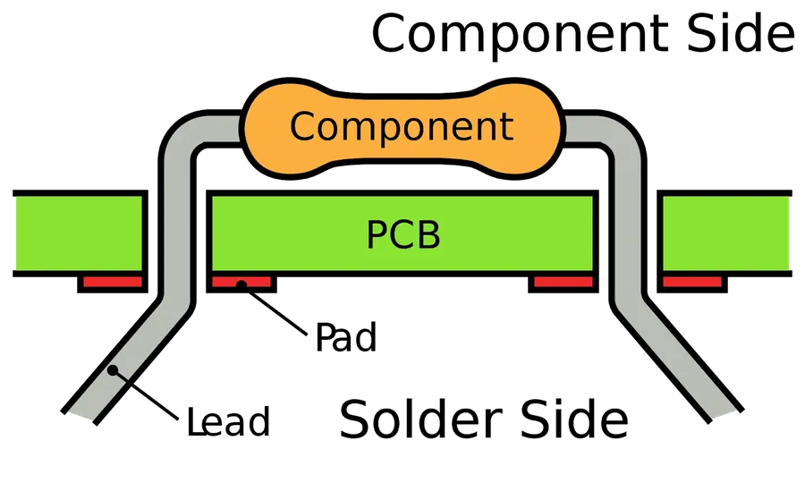
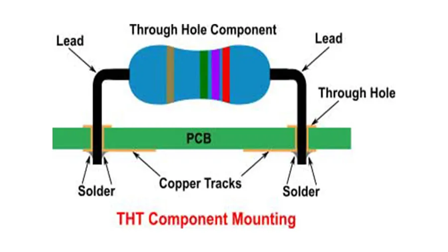
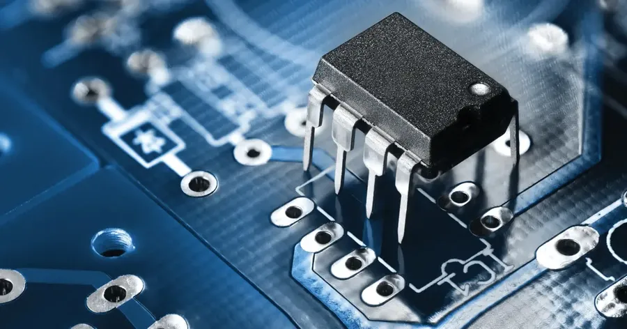
Through-hole technology (THT) is a fundamental method in electronics manufacturing where component leads are inserted into pre-drilled holes on a printed circuit board (PCB) and subsequently soldered in place. This method, one of the earliest PCB assembly techniques, provides robust mechanical connections and secure electrical paths.
The historical roots of through-hole technology lie in the early days of electronics manufacturing when circuit boards were largely hand-assembled. Components with leads extending from their bodies were inserted into holes and then soldered on the opposite side to secure them. This method proved effective for both prototyping and mass production and continues to be utilized today.
The core principle of THT involves creating a physical connection between a component and a PCB through drilled holes, which are typically plated to enhance electrical conductivity. The component lead is passed through the hole and soldered to the pad on the opposite side of the board, establishing both an electrical and mechanical bond.
Plated Through-Holes (PTH) vs. Non-Plated Through-Holes (NPTH)
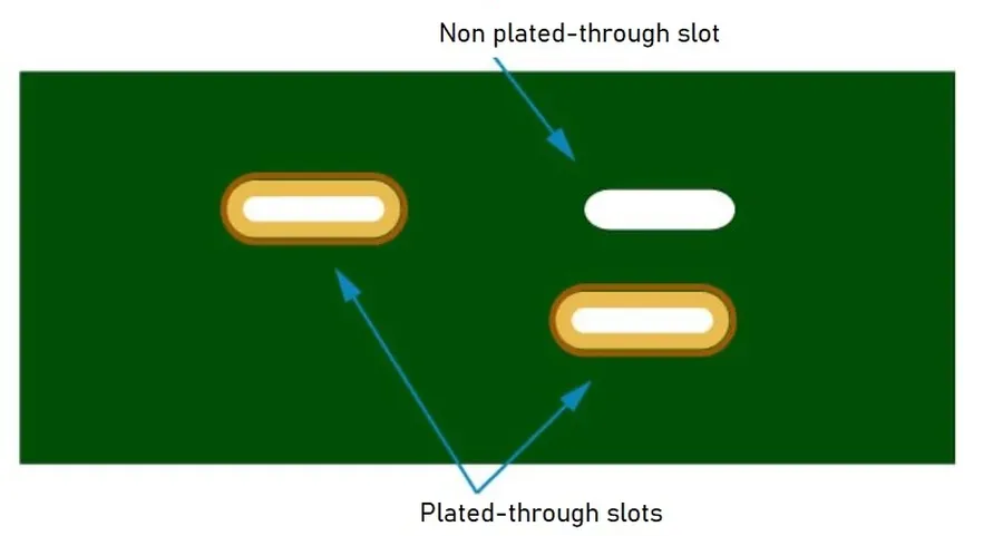
Printed Circuit Boards (PCBs) utilize both Plated Through-Holes (PTH) and Non-Plated Through-Holes (NPTH), each serving distinct purposes crucial to PCB functionality. PTHs provide electrical connectivity between different layers of a multi-layered PCB, while NPTHs are primarily used for mechanical mounting or alignment, without electrical connection. Understanding their differences is fundamental for effective PCB design and assembly.
| Feature | Plated Through-Hole (PTH) | Non-Plated Through-Hole (NPTH) |
|---|---|---|
| Electrical Connection | Yes, provides vertical electrical pathways between layers | No, does not facilitate electrical conductivity |
| Plating | Hole walls are plated with conductive material (e.g., copper) | Hole walls are not plated, typically bare substrate material |
| Primary Function | Electrical interconnection and component mounting | Mechanical mounting, alignment, or clearance |
| Usage | For component leads, vias, and interlayer connections | For mounting hardware, locating pins, or structural support |
| Cost | Higher, due to the additional plating process | Lower, as it avoids the plating process |
The choice between PTH and NPTH depends heavily on the specific requirements of the PCB design. PTH is indispensable in multi-layer PCBs for ensuring reliable electrical connections across different layers. In contrast, NPTHs are selected when electrical conductivity is not required and when mechanical stability is paramount. For example, mounting holes for securing a PCB within an enclosure typically utilize NPTH to save on manufacturing cost and complexity.
The Through-Hole Assembly Process: A Step-by-Step Guide
The assembly of through-hole PCBs is a structured process that, when followed carefully, ensures reliable electrical connections and mechanical stability. This section details each step, from preparing components to the final soldering and inspection.
- Component Preparation
Begin by gathering all necessary components, ensuring they are correctly identified according to the Bill of Materials (BOM). Inspect components for any physical damage. If necessary, leads may need to be straightened or pre-formed to facilitate insertion into the PCB. - Component Insertion
Carefully insert the components into their designated through-holes on the PCB. Ensure the correct orientation of polarized components, such as diodes and electrolytic capacitors, as incorrect placement can cause circuit malfunctions. For components with long leads, consider using a component insertion tool or a manual lead bender to facilitate accurate placement. - Lead Securing
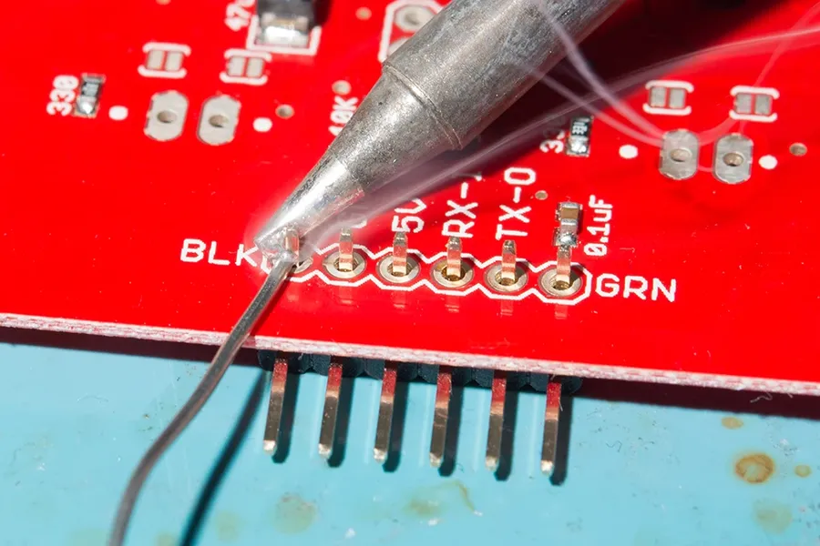
After insertion, bend leads outward on the solder side of the board to temporarily secure components. This prevents them from falling out during handling and during the following solder process. This technique is especially useful for through hole components that may be mounted vertically. - Soldering
Solder each component lead to the pad on the solder side of the PCB. Use a soldering iron with a suitable tip, temperature, and solder alloy appropriate for the task. Ensure that each solder joint is smooth, shiny, and free of cold solder joints or solder bridges. Apply heat to both the pad and the component lead, then feed solder to achieve a good joint, using the principle of solder flow through thermal conduction. - Lead Trimming
Once soldering is complete, trim excess lead length using lead cutters. Ensure the leads are trimmed close to the solder joint, while avoiding damage to the solder. This is essential for preventing short circuits and ensuring there is adequate clearance in the final product housing. Use a lead cutter that is designed to cut leads with minimal force. - Cleaning
Clean the soldered PCB with a suitable cleaning solution and brush to remove any flux residue, or other contaminants. Residual flux can cause corrosion and affect reliability of the circuit. Ensure proper ventilation while using these solutions. Use a lint-free cloth to dry the board completely after cleaning. - Inspection
Perform a thorough visual inspection of all solder joints, using magnification if needed. Look for issues like insufficient solder, excess solder, cold solder joints, solder bridges, and proper lead trimming. Verify the component placement and correct component orientation. Electrical testing is recommended after final inspection to verify board function.
Through-Hole PCB Design Rules and Considerations

Designing reliable and functional through-hole PCBs necessitates adherence to specific rules and careful consideration of various factors. These guidelines ensure proper component placement, secure mechanical mounting, and optimal electrical performance. Key considerations include hole size, pad design, and component spacing, each directly impacting the manufacturability and long-term reliability of the final product. Ignoring these rules can lead to assembly issues, decreased performance, and even catastrophic failures.
| Design Rule | Description | Importance |
|---|---|---|
| Hole Diameter | The size of the drilled hole for component leads. | Ensures proper component fit and solder joint integrity. Insufficient clearance can damage leads during insertion; excessive clearance can lead to poor solder joints. |
| Pad Size and Shape | The copper area surrounding the hole, for soldering. | Critical for solder joint strength and thermal dissipation. Optimizing shape and size ensures reliable electrical connection and prevents issues such as tombstoning during reflow. |
| Pad to Trace Clearance | The space between the pad and any adjacent copper traces. | Prevents short circuits and ensures proper electrical isolation. Insufficient clearance can lead to unintended current paths and device malfunction. |
| Component Spacing | The physical distance between adjacent through-hole components. | Facilitates manual and automated assembly, ensuring sufficient clearance for tools and preventing interference. Adequate space also allows for rework, if needed. |
| Drill Registration | The accuracy of hole placement during drilling. | Ensures that holes align correctly with component leads and pads. Poor registration can cause manufacturing defects and assembly challenges. |
| Annular Ring | The width of copper pad surrounding a plated through-hole (PTH) after drilling | Ensures electrical connection and mechanical strength. It prevents the drill hole from breaking through the copper pad and guarantees a reliable solder joint. |
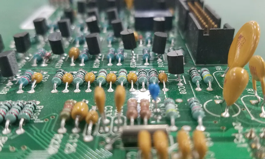
Through-Hole Components: Types and Applications
Through-hole components, characterized by their leads that are inserted into drilled holes on a PCB and soldered on the opposite side, are fundamental to electronics design and assembly. This technology allows for robust mechanical connections, making it suitable for applications requiring high reliability and durability. This section details the diverse types of through-hole components and their specific applications, highlighting their advantages in various electronic systems.
| Component Type | Description | Typical Applications | Advantages |
|---|---|---|---|
| Resistors | Passive components that provide a specific resistance to current flow. Commonly used for current limiting, voltage division, and signal termination. | Power supplies, amplifier circuits, signal processing units. | Wide range of resistance values, robust handling, easy to test |
| Capacitors | Passive components that store electrical energy in an electric field. Used for filtering, energy storage, and timing circuits. | Power smoothing, signal coupling, bypass circuits, filter circuits. | Variety of capacitance values, different dielectric materials available |
| Diodes | Semiconductor devices that allow current flow in one direction. Used for rectification, signal detection, and voltage regulation. | Rectifier circuits, voltage clamps, signal demodulation. | Robust and reliable, good for high-voltage and high-current circuits |
| Transistors | Semiconductor devices used to amplify or switch electronic signals and electrical power. Used as amplifiers and switches. | Amplifier stages, switching power supplies, logic circuits. | Versatile for analog and digital applications |
| Integrated Circuits (ICs) | Complex circuits fabricated on a single semiconductor chip. Perform specific functions such as microprocessing, memory management, and signal conditioning. | Microcontrollers, memory modules, logic gates, op-amps. | High integration density, complex functionality |
| Connectors | Devices that facilitate the joining of electronic circuits and other hardware. Allow for modular designs and easy replacement of parts. | Input/output interfaces, power connections, board-to-board connections. | Variety of connection types available for specific functions, robust connections |
| Inductors | Passive components that store energy in a magnetic field. Used for filtering, tuning circuits, and impedance matching. | Power supplies, resonant circuits, filter circuits. | Good for high-current applications, variety of inductance values |
Through-Hole vs. Surface Mount Technology (SMT): A Comparative Analysis

Through-hole technology (THT) and surface mount technology (SMT) represent the two dominant methods for mounting electronic components onto printed circuit boards (PCBs). This section provides a direct comparison of these two technologies, analyzing their respective strengths, weaknesses, and application suitability, thereby enabling engineers to make informed decisions based on their project requirements.
| Feature | Through-Hole Technology (THT) | Surface Mount Technology (SMT) |
|---|---|---|
| Component Mounting | Component leads inserted into drilled holes on PCB. | Components soldered directly onto the surface of PCB. |
| Mechanical Strength | Provides high mechanical strength due to component leads through the board. | Generally lower mechanical strength but can be improved by robust pad design and materials. |
| Assembly Process | Requires manual or automated through-hole insertion and soldering. | Highly automated pick-and-place and reflow soldering process. |
| Component Size | Generally larger components, often with leaded packages. | Allows for miniaturized components and high-density designs. |
| Component Density | Lower component density due to space required for holes and leads. | Higher component density on PCB enabling miniaturization of the design. |
| Manufacturing Cost | Higher cost for mass production due to the need for drilling and through-hole component mounting. | Lower cost for mass production due to automated assembly process and standardized components. |
| Thermal Performance | Better thermal performance for high-power devices due to component leads acting as heat sinks. | Requires careful thermal design, especially for power-intensive applications. |
| Ease of Prototyping | More suitable for prototyping and hobbyist projects due to ease of manual assembly. | Can be more challenging for prototyping without specialized equipment. |
| Rework and Repair | Easier to rework and repair using standard soldering equipment. | Requires specialized equipment and expertise for rework. |
| Applications | Suitable for robust applications where mechanical strength is critical, and for prototyping and hobbyist use. | Ideal for mass-produced consumer electronics, high-density designs and high frequency designs. |
Frequently Asked Questions About Through-Hole PCBs
This section addresses common queries regarding through-hole PCB technology, offering clear explanations and comparisons to surface mount technology (SMT). It aims to resolve any uncertainties and provide a solid understanding of through-hole PCB design and application.
- What exactly is a through-hole in a PCB?
A through-hole in a PCB is a hole that is drilled through the entire thickness of the board, intended for the insertion and soldering of component leads. These holes can be plated (PTH) or non-plated (NPTH) depending on their function. - What is the term used for the through-hole connection on a PCB?
The through-hole connection is commonly referred to as a 'via' when used to connect layers of a multi-layer PCB or simply a 'through-hole' when used for mounting components. - What differentiates a through-hole PCB from a surface mount (SMT) PCB?
The key difference lies in component mounting. Through-hole PCBs have components with leads that pass through drilled holes and are soldered on the opposite side of the board, offering a stronger mechanical bond, while SMT components are soldered directly onto the surface of the PCB, often leading to smaller and more compact designs. Through-hole technology provides greater strength in mechanical bonding of parts, while surface mount is generally used for higher speed circuits. - What purpose does a through-hole serve in a PCB?
The main purpose of a through-hole is to provide a secure mounting point for electronic components, creating a robust mechanical and electrical connection. They are crucial for parts that require high reliability, such as connectors, large capacitors, or parts that undergo stress. - When is through-hole technology preferred over SMT?
Through-hole technology is preferred when high mechanical strength, reliability under stress, or easy prototyping is required. It's also suitable for larger components or those that need to withstand physical forces. It is also often preferred by hobbyists due to its ease of manual soldering. - Can through-hole and SMT components be mixed on the same PCB?
Yes, it is very common to find PCBs that utilize both through-hole and SMT components to leverage the benefits of both technologies. For example, larger or mechanically stressed parts can be through-hole and smaller components can be surface mount to save board space and fabrication cost. - How are through-hole components soldered to a PCB?
Through-hole components are generally soldered manually, wave-soldered, or reflow-soldered (for parts with through hole leads exposed to a solder paste). Manual soldering is done using a soldering iron. Wave soldering is a process used in mass production where the boards pass through a wave of molten solder. Reflow soldering is an SMT process but is occasionally used for some through-hole parts when solder paste is used around component leads.
Advanced Applications and Future Trends in Through-Hole Technology
While surface mount technology (SMT) dominates modern electronics, through-hole technology continues to thrive in specialized and high-reliability applications. Its inherent robustness and mechanical strength offer distinct advantages where physical durability is paramount. This section will explore these niche applications and speculate on the future evolution of through-hole technology.
Through-hole components are still heavily utilized in several critical sectors, particularly where robust connections and high power handling are essential. These applications leverage the physical strength of through-hole mounting, providing a far more secure connection than SMT components in demanding operating environments. As technology continues to evolve, through-hole maintains its relevance and applicability in areas where absolute reliability and durability are key requirements.
- Aerospace and Military Applications
In aerospace and military hardware, through-hole components are preferred due to their exceptional resistance to mechanical stresses, vibration and extreme temperatures. Connectors, high-current components, and certain types of sensors often rely on through-hole mounting for absolute connection reliability. Given the critical operational nature of these systems, the robust connection offered by through-hole is non-negotiable. - High-Power Electronics
Power supplies, inverters, and motor control circuits often require components capable of handling high currents and voltages. Through-hole components, such as high-wattage resistors, large capacitors, and transformers, are commonly used in these applications because of their superior heat dissipation and robust connection, which is necessary for the reliable operation of high-power electronics, where SMT components could be less robust. - Industrial Control Systems
Industrial settings often subject electronics to harsh environments, which can include extreme temperatures, humidity, vibration, and chemical exposure. Through-hole components are favored in control systems, heavy machinery, and process automation due to their mechanical robustness and resistance to disconnection from their pads under duress. This reliability is critical for continuous and dependable industrial operations. - Prototyping and Experimentation
For prototyping and testing phases of new electronic devices, through-hole technology provides ease of manipulation, allowing easier component changes on prototype boards. The larger size of through-hole components and their compatibility with breadboards make them a good choice for early-stage device development. This adaptability makes through-hole a convenient option in research and development.
Looking ahead, while SMT continues to dominate in miniaturization, the longevity of through-hole technology remains secured by its inherent advantages. The future will likely see a consolidation of through-hole applications within those areas requiring its distinct advantages, while SMT will continue in the mass production of portable electronics. A future trend may see materials development to enhance through-hole components' high temperature and vibrational tolerance even further.
The future of through-hole technology may also see the development of hybrid mounting techniques combining the strengths of both SMT and through-hole on a single board. Such boards may utilise SMT for standard components and reserve through-hole mounting for critical and higher power components. The future will likely see a synergistic approach to PCB design that leverages both SMT and through-hole technologies.
Best Practices for Through-Hole PCB Soldering and Inspection
Ensuring high-quality soldering for through-hole components is crucial for the reliability and longevity of electronic devices. This section outlines essential techniques and inspection methods to achieve robust solder joints and avoid common soldering pitfalls.
- Preparation is Key
Prior to soldering, ensure that both the component leads and the PCB pads are clean and free of oxidation. Use a suitable flux to promote solder flow and wetting, which are essential for creating strong, conductive joints. - Selecting the Right Soldering Equipment
Utilize a temperature-controlled soldering iron with an appropriately sized tip for the components being soldered. A fine tip is suitable for smaller components, while a larger tip is better for larger ones, and the selection of the solder wire diameter should match with the component pad sizes. Employ high-quality solder wire with a flux core to ensure reliable connections. - Temperature Control
Proper temperature control is crucial. Too low temperature will lead to cold solder joints (weak connections), while too high temperature may damage the components or the board. A temperature between 320°C to 370°C is generally suitable for tin-lead solder or lead-free solders. For components sensitive to heat, adjust temperature accordingly and minimize heat exposure time. - The Soldering Process
Heat both the component lead and the PCB pad simultaneously, then apply the solder to the heated area. Allow the solder to flow evenly around the lead and pad, forming a smooth, concave fillet. Avoid moving the joint during cooling to prevent disturbing the connection. - Avoid Overheating
Excessive heat can damage components and PCB materials. Heat the joint only long enough to create a solid connection. If a joint does not form well, allow the board to cool before trying again. Use solder paste for reflow soldering for better control and consistency. - Visual Inspection
After soldering, visually inspect each joint. A good solder joint should appear smooth, shiny, and have a concave shape, indicating good wetting. The solder should evenly cover the pad and the component lead. - Common Soldering Defects to Avoid
Look out for common soldering defects such as cold solder joints (dull, grainy appearance), solder bridges (solder shorting between pads), insufficient solder (not enough solder to create a full connection), and excess solder (excessive solder that can potentially cause shorts). Use a magnifying glass or microscope for detailed examination. - Proper Cleaning and Maintenance
After soldering and inspection is complete, clean the PCB with a suitable cleaning agent such as isopropyl alcohol (IPA) to remove any residual flux. This step is important to prevent corrosion and ensure reliable performance. Store the boards in a dry and clean environment to prevent oxidization.
Through-hole PCB technology, despite the rise of SMT, remains a critical part of electronic manufacturing, offering robustness and reliability where it matters most. Understanding its nuances, from design principles to assembly techniques, is essential for anyone involved in PCB development. This guide provides a foundational knowledge, with practical insights and considerations for leveraging the full potential of through-hole technology in modern electronic designs. As we continue to innovate, it is crucial to recognize the legacy and ongoing value of this foundational method.