OSH Park: Your Guide to High-Quality PCB Prototyping
In today's world, where electronics are woven into the fabric of our daily lives, the need for reliable and accessible printed circuit board (PCB) prototyping services is paramount. Enter OSH Park, a US-based company that has revolutionized the way designers and hobbyists access high-quality, lead-free PCBs. This article will delve into what makes OSH Park a valuable resource, offering a comprehensive guide to their services and how they can benefit your next electronic project.
What is OSH Park?
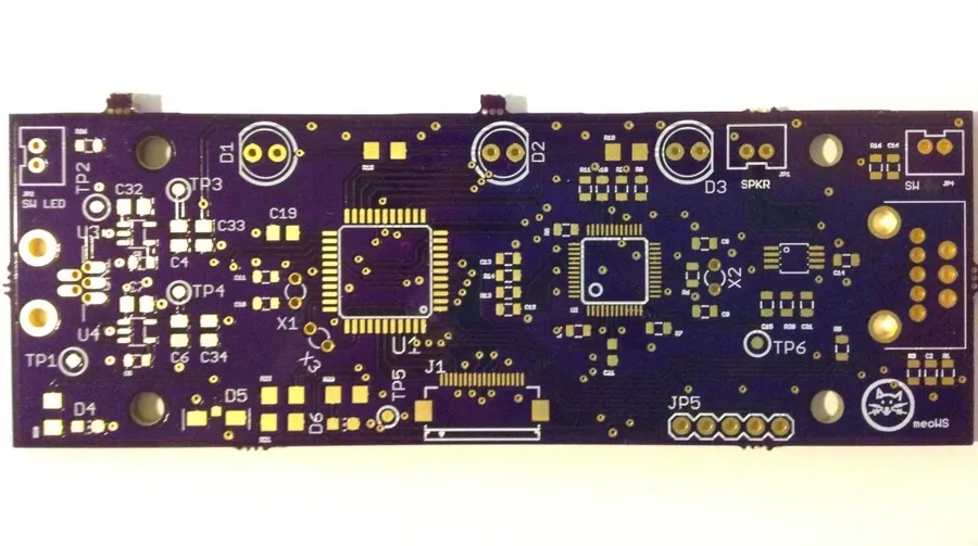
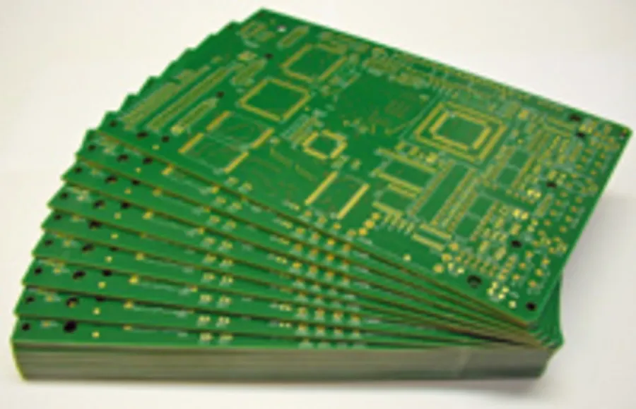
OSH Park is a distinctive printed circuit board (PCB) fabrication service that operates on a community-driven model. It ingeniously combines multiple users' PCB designs onto a shared manufacturing panel. This method significantly reduces costs, making it an ideal solution for both prototyping and small-batch PCB production. By sharing the fabrication expenses, OSH Park provides access to high-quality PCBs at budget-friendly prices, appealing to hobbyists, makers, and professionals alike.
The OSH Park Manufacturing Process
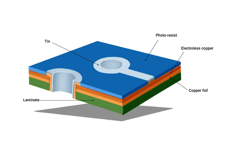
OSH Park employs a unique manufacturing model centered around panelization, where multiple customer PCB designs are aggregated onto a single, larger manufacturing panel. This approach allows for a significant reduction in per-board costs by distributing the overhead associated with fabrication across multiple orders.
The core of OSH Park's efficiency lies in its aggregation process. Instead of manufacturing individual PCBs, they combine various customer designs onto a standardized panel. This panel is then processed through the PCB fabrication steps including etching, drilling, and plating.
The fabrication process is typically carried out in the United States to ensure high quality standards. However, to accommodate production demands and variations in customer orders, OSH Park may strategically outsource some manufacturing to trusted partners that adhere to their rigid standards of quality and precision.
- Panelization
Customer designs are combined onto a single panel, optimizing the use of raw materials. - Cost Sharing
Manufacturing costs are shared among multiple orders, lowering the price per PCB. - Fabrication Location
Primarily manufactured in the USA, with some outsourcing to maintain capacity and quality.
| Process Step | Description |
|---|---|
| Design Submission | Customers upload their PCB designs as Gerber files. |
| Panelization | Designs are combined into a panel suitable for manufacturing. |
| Fabrication | The panel undergoes the PCB manufacturing process, including etching, drilling, and plating. |
| Separation | Individual PCBs are separated from the panel. |
| Quality Control | Each PCB is inspected to meet OSH Park standards. |
| Shipping | The manufactured PCBs are shipped to customers. |
OSH Park's PCB Capabilities
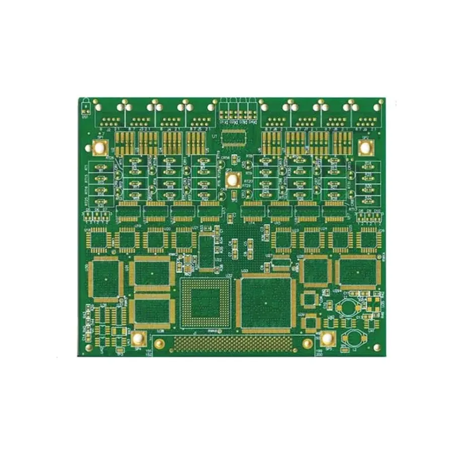
OSH Park specializes in providing high-quality, cost-effective PCB fabrication services, primarily focusing on two-layer and four-layer boards suitable for a wide range of prototyping and small-batch production needs. Their offerings are tailored to the maker community and small businesses requiring reliable PCB fabrication.
| Feature | 2-Layer PCB | 4-Layer PCB |
|---|---|---|
| Typical Use Cases | Simpler circuits, hobbyist projects, basic prototypes | More complex circuits, designs requiring signal and power routing on multiple layers |
| Material | Standard FR-4 | Standard FR-4 |
| Layer Count | 2 Copper Layers | 4 Copper Layers |
| Board Thickness | 1.6mm (0.063") | 1.6mm (0.063") |
| Copper Weight | 1 oz/ft² (standard) | 1 oz/ft² (standard) |
| Surface Finish | ENIG (Electroless Nickel Immersion Gold) | ENIG (Electroless Nickel Immersion Gold) |
| Minimum Track/Spacing | 6 mil (0.1524 mm) | 6 mil (0.1524 mm) |
It is important to note that OSH Park has specific design rules, such as minimum track widths, clearances, and via sizes, that must be adhered to for successful fabrication. Refer to the OSH Park design rules for detailed specifications.
OSH Park Design Rules and Guidelines
Adhering to OSH Park's specific design rules and guidelines is paramount for ensuring the successful fabrication of your printed circuit boards (PCBs). These rules are tailored to their manufacturing processes and equipment, and deviation can lead to errors in production or unusable boards. Understanding and applying these parameters from the outset of your design process will save time and resources.
| Parameter | 2-Layer Boards | 4-Layer Boards |
|---|---|---|
| Minimum Trace Width | 6 mil (0.1524 mm) | 6 mil (0.1524 mm) |
| Minimum Clearance | 6 mil (0.1524 mm) | 6 mil (0.1524 mm) |
| Minimum Via Drill Size | 13 mil (0.3302 mm) | 13 mil (0.3302 mm) |
| Minimum Annular Ring | 5 mil (0.127 mm) | 5 mil (0.127 mm) |
| Maximum Board Size | 12" x 18" | 12" x 18" |
| Copper Thickness | 1 oz | 1 oz |
| Material | FR4 | FR4 |
- Layer Stack-up
For 4-layer boards, OSH Park uses a specific stack-up; it's recommended to refer to their documentation to understand signal, ground, and power layer placement. The correct layering ensures optimal signal integrity and power distribution. The two layer board has the signal layers on the top and the bottom with the core material in the middle. - Gerber File Preparation
OSH Park accepts standard Gerber RS-274X files along with Excellon drill files. Be sure to include all necessary layers (copper, soldermask, silkscreen), and ensure your drill files are in the correct format. Properly formatted Gerber files are critical to avoid manufacturing delays and errors. - Board Outline
Your board outline must be clearly defined, typically on a separate layer. Ensure that the outline is closed and does not contain any intersecting lines. - Copper Features
Avoid copper fills or traces that are too close to the board's edge, it may result in issues during manufacturing. It's best to maintain a reasonable clearance to the board outline for best results.
Always cross-reference the latest design rules on the OSH Park website as they may be updated periodically. By adhering to these standards and thoroughly preparing your design files, you can significantly improve the likelihood of a successful PCB fabrication process.
How to Order PCBs from OSH Park
Ordering printed circuit boards (PCBs) from OSH Park is a straightforward process designed to be accessible for both hobbyists and professionals. This section provides a detailed guide on how to submit your PCB designs, from preparing your Gerber files to tracking your order, ensuring a seamless experience.
- Prepare Your Gerber Files
Before submitting to OSH Park, ensure your PCB design software outputs Gerber files (RS-274X format) and an Excellon drill file. These files are the industry standard for PCB manufacturing. Verify that all layers, including copper layers, solder mask, silkscreen, and drill data, are generated correctly. OSH Park recommends using the latest Gerber format, RS-274X, for compatibility. It is crucial to check your Gerber files with a viewer to identify any issues before submission. - Navigate to the OSH Park Website
Go to the OSH Park website, where you will find a user-friendly interface for uploading your designs. Create an account or log in if you're a returning user. The ordering process is initiated by clicking on the 'Upload' or 'Order' button. - Upload Your Gerber Files
Upload all necessary Gerber files as a ZIP archive. OSH Park's system automatically detects and interprets the necessary files, but it's crucial to verify the correct selection before proceeding. Ensure no files are missing or corrupted in the archive. The system will analyze the files to confirm the number of layers and board dimensions. - Review Your PCB Preview
After uploading, OSH Park generates a preview of your PCB design, which you must carefully examine. Confirm the correct board outline, copper traces, pads, vias, and other elements are displayed as expected. This step is critical to catch potential errors before manufacturing. Pay close attention to the scale, layer alignment, and any areas that may seem incorrect or unexpected. This review is the last opportunity to catch design flaws. - Select Your Options and Place Order
OSH Park offers limited options, with only standard 2-layer or 4-layer options. Select the board quantity you require, and you'll receive a real-time cost estimate. Finalize your order by adding it to your cart and completing the checkout process. Double-check your shipping address and payment method to avoid any delays. - Track Your Order
Once your order is placed, OSH Park provides a tracking number to monitor its progress. You’ll receive updates on the manufacturing status and estimated delivery times. OSH Park usually batches orders, so there might be some delay between order placement and the start of production. It's important to periodically check the tracking information to be informed of any status changes.
Frequently Asked Questions About OSH Park
This section addresses common questions regarding OSH Park, providing clarity on their services, processes, and user experience. These questions are designed to tackle the common pain points and curiosities of new and existing users.
- Where is OSH Park located?
OSH Park's primary operations are based in the United States. While they do not have public-facing retail locations, their manufacturing and shipping are coordinated from within the USA. This central location allows them to maintain quality control and efficient delivery. - Is OSH Park a legitimate PCB manufacturing service?
Yes, OSH Park is a well-established and reputable PCB manufacturing service. They are widely recognized within the hobbyist and professional electronics community for their high-quality boards and reliable service. OSH Park has garnered significant positive feedback and is considered a trustworthy vendor for PCB fabrication. - What types of PCBs does OSH Park offer?
OSH Park primarily offers 2-layer and 4-layer PCBs. Their standard service provides a set of highly reliable, economical boards with options that cater to both simple and moderately complex designs. They use a consistent set of high-quality materials and manufacturing processes across their offerings. - How long does OSH Park typically take to deliver PCBs?
OSH Park's turnaround time varies based on order volume and fabrication complexity, but it generally ranges from 1 to 3 weeks from the time the order is placed. The typical delivery is within 10-15 business days. Factors like panelization and shipping time can affect this timeframe, but they maintain transparency throughout the process. - What file formats does OSH Park accept for PCB designs?
OSH Park requires Gerber files for submitting PCB designs. These files are an industry standard for PCB fabrication and include information on all the layers of your board as well as the drill information. Make sure all your necessary Gerber files are generated correctly from your EDA software and that they meet OSH Park's design rules to avoid delays. - What are the minimum trace widths and clearances I need to consider?
For 2-layer boards, OSH Park's minimum trace width and clearance are 6 mils (0.1524 mm). For 4-layer boards, these values are often slightly tighter at 5 mils (0.127mm). It's crucial to adhere to these specifications, as failing to do so could result in fabrication errors. - Does OSH Park offer assembly services?
Currently, OSH Park focuses solely on PCB fabrication and does not provide assembly services. Users receive the bare PCBs and must manage component placement and soldering themselves or utilize separate assembly services. This focus on fabrication allows OSH Park to optimize their manufacturing process and maintain quality.
Comparing OSH Park to Other PCB Services
When selecting a PCB fabrication service, it's crucial to evaluate several factors, including cost, turnaround time, quality, and specific capabilities. OSH Park distinguishes itself with its unique panelization approach, which can significantly reduce costs, especially for small runs. However, understanding how it stacks up against other services is essential for making the right decision based on your specific needs. This analysis provides a comparison of OSH Park with alternative PCB fabrication services, focusing on the advantages and disadvantages of each.
| Feature | OSH Park | Other PCB Services (e.g., JLCPCB, PCBWay) |
|---|---|---|
| Pricing | Cost-effective for small runs due to panelization; fixed price per board area regardless of quantity within a panel | Variable pricing; often cheaper for larger quantities but more expensive for very small runs |
| Turnaround Time | Moderate; can be longer due to panelization and batch manufacturing; typically 1-3 weeks | Faster turnaround times, often within a week, with express options available |
| Quality | High-quality boards manufactured in the US, with standard 2-layer and 4-layer options; consistent quality | Quality varies, generally good, but may vary depending on the manufacturer's options selected; also offer higher layer counts and more material selections |
| Capabilities | Limited to 2 and 4 layer boards; standard materials; focus on prototyping needs | Broader range of options; more layer counts, advanced materials, tighter tolerances |
| Ordering | Direct upload of Gerber files; no order quantity specification; panelization is automatic. | Offers more control over order quantities, options, and customization, may require specific files. |
| Customer Support | Community-focused support, slower responses | Often offers faster and more direct customer support |
- When to Choose OSH Park:
Consider OSH Park if your needs include: small-run prototyping, affordability is a priority, and your design fits within their standard specifications. It's ideal for projects that are not time-sensitive and prioritize quality. - When to Consider Other Services:
Other services might be better suited for projects with specific requirements such as: higher layer counts, specialized materials, faster turnaround times, and if you need larger production runs.
OSH Park for Beginners: Essential Tips and Guidance
Getting started with PCB design and fabrication can be daunting for newcomers. This section offers essential tips and guidance to help beginners navigate the OSH Park service smoothly, focusing on design best practices and troubleshooting common issues that might arise during the process.
- Start with Simple Designs
Begin with basic 2-layer designs to familiarize yourself with the design process, software, and OSH Park's specific requirements. Avoid complex multilayer designs until you've gained experience. - Understand Design Rules
Thoroughly review and understand OSH Park's design rules before starting your design. Pay close attention to minimum trace widths, clearances, via sizes, and drill specifications, as these are critical for successful fabrication. Failure to adhere to these will result in unusable PCBs. - Use a Reliable EDA Software
Select an Electronic Design Automation (EDA) software you are comfortable with and which supports exporting Gerbers that are compatible with OSH Park. KiCad, EasyEDA, and Eagle are popular choices that offer good capabilities. Use a software that you understand well. - Double-Check Your Gerber Files
Before submitting your design, meticulously inspect your generated Gerber files using a Gerber viewer. Verify all layers, drill holes, and outlines for errors. This step is crucial to identify design errors before they are fabricated. - Test Small Batches
For initial designs, order a small quantity of boards to test them thoroughly before committing to a large order. This allows you to validate your design and make changes as needed, without excessive cost. - Join the Community for Support
Engage with the OSH Park community on forums and social media platforms. There are many experienced users who can provide valuable advice and assistance with any issues you encounter. It's a valuable source of knowledge and real-world advice. - Start with Example Projects
Look for existing open-source projects that use OSH Park. Reviewing and understanding such designs provides insight into best practices and helps avoid common mistakes.
OSH Park: Community and Beyond
OSH Park's strength extends beyond its PCB fabrication services; it's deeply rooted in a vibrant and active community. This community-centric approach fosters a collaborative environment where makers, engineers, and hobbyists share knowledge, inspiration, and support, creating a space where innovation thrives.
The OSH Park community actively engages across multiple platforms, providing an invaluable resource for both newcomers and seasoned professionals. This communal spirit helps users maximize their experience with OSH Park and promotes continuous learning and project development within the hardware engineering community. Through this active participation, users find more than just a PCB fabrication service; they find a collaborative partner in their design and prototyping journeys.
- Community Forums and Discussions
Many online platforms host active discussions about OSH Park. These forums are a goldmine for users seeking advice, troubleshooting assistance, and project inspiration. These community spaces allow both novice and expert users to share their experiences with OSH Park, leading to a robust pool of collective knowledge. Users frequently share innovative ideas and successful projects, sparking creativity and supporting other members. - Social Media Engagement
OSH Park has a considerable presence on various social media platforms. Following these accounts provides up-to-date information about the service and opportunities for networking. Social media channels are also a valuable platform for showcasing user projects, creating a dynamic space for inspiration and engagement, which adds to the overall experience of using OSH Park. - Inspiration and Project Showcases
Many users showcase their OSH Park-fabricated PCB projects online. Platforms like Reddit and personal blogs are full of great examples of projects that other users have completed. These showcases serve as inspiration and a demonstration of the possibilities that the platform provides. - Collaborative Project Development
The OSH Park community often collaborates on projects, from open-source hardware designs to group buys for components. Such joint ventures promote knowledge sharing and allow many makers to bring projects to life. This collaborative spirit makes OSH Park not just a PCB service but also a hub for collective innovation.
OSH Park stands as a reliable and accessible service for hobbyists, designers, and small businesses seeking high-quality PCB prototypes. Their unique approach to panelizing orders allows them to offer cost-effective solutions while maintaining excellent quality. Whether you're starting a new project or refining an existing one, OSH Park provides a valuable resource to bring your electronic creations to life. Consider OSH Park for your next PCB project and experience the difference for yourself. By understanding their process, design rules, and community, you'll be well-equipped to take full advantage of their services.