PCBWay: Your Comprehensive Guide to PCB Manufacturing & Assembly
In today's tech-driven world, the unassuming Printed Circuit Board (PCB) is the unsung hero behind almost every electronic device. From your smartphone to complex industrial machinery, PCBs form the foundation of modern technology. PCBWay stands at the forefront of PCB manufacturing and assembly, transforming innovative designs into tangible products. This article will provide a comprehensive look at PCBWay's offerings, guiding you through their services and processes, and showing you how they connect with the pulse of global innovation.
Overview of PCBWay's Services
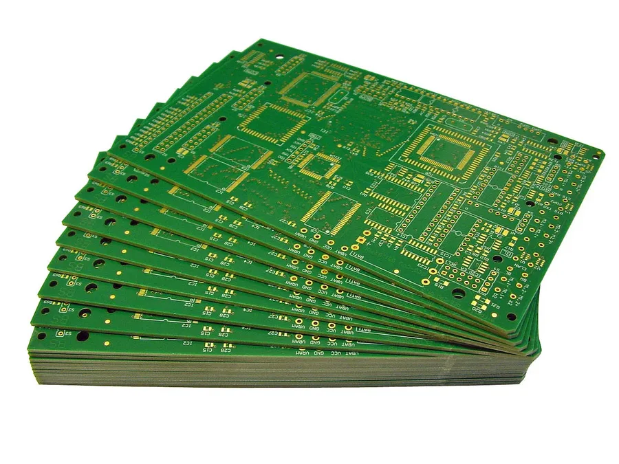
PCBWay provides a comprehensive suite of services encompassing the entire lifecycle of printed circuit board (PCB) development, from initial prototyping to mass production and assembly. Their offerings are tailored to meet diverse project requirements, catering to individual engineers, small businesses, and large corporations alike. The core of PCBWay's services lies in its ability to rapidly fabricate PCBs with a high degree of precision and quality.
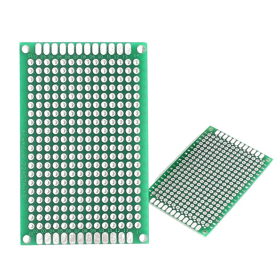
- PCB Prototyping
This service allows for the creation of small quantities of PCBs for testing and validation purposes. It is ideal for iterating on designs quickly and cost-effectively. - Small-Batch PCB Production
PCBWay facilitates small to medium production runs for projects that require more PCBs than prototyping but don't necessitate full-scale mass production. - Large-Scale PCB Assembly
For projects that have passed the prototyping phase and are ready for market, PCBWay provides PCB assembly, ranging from simple surface mount to more complex through-hole components.
PCB Prototyping with PCBWay
PCBWay's prototyping services are engineered to facilitate the rapid and cost-effective realization of initial PCB designs. The service encompasses a wide spectrum of options, including diverse materials, varied layer counts, and specialized surface finishes, all critical for verifying design concepts before large-scale production.
| Feature | Description | Typical Application |
|---|---|---|
| Material Options | Includes FR-4, Aluminum, Flexible, and High-Frequency materials. | Diverse applications ranging from standard circuits to high-speed signal processing and flexible electronics. |
| Layer Counts | Range from single-layer to complex multi-layer boards. | Accommodates simple circuits and complex high-density interconnects. |
| Special Finishes | Options like ENIG, HASL, Immersion Tin, and OSP. | Ensures solderability, corrosion resistance, and optimal electrical performance. |
| Turnaround Time | Rapid prototyping with efficient manufacturing processes. | Quick validation of design and faster time-to-market for projects. |
The selection of appropriate materials and finishes in the prototyping phase is critical. For instance, FR-4 is ideal for general purpose prototyping, while materials like Rogers are better suited for high frequency applications. Similarly, ENIG (Electroless Nickel Immersion Gold) provides excellent solderability and corrosion resistance, making it a popular choice for prototypes intended for extended testing and further development.
PCBWay's rapid prototyping service allows engineers and designers to efficiently iterate on their designs, ensuring a smoother transition from concept to mass production. The ability to quickly receive prototypes enables early testing and design validation, mitigating the risk of costly issues during large-scale manufacturing.
PCB Assembly Services at PCBWay
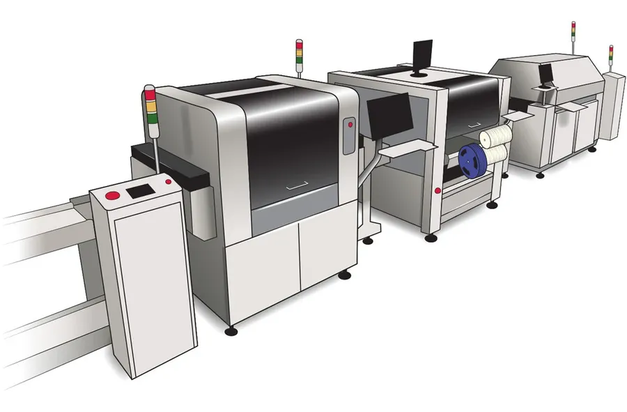
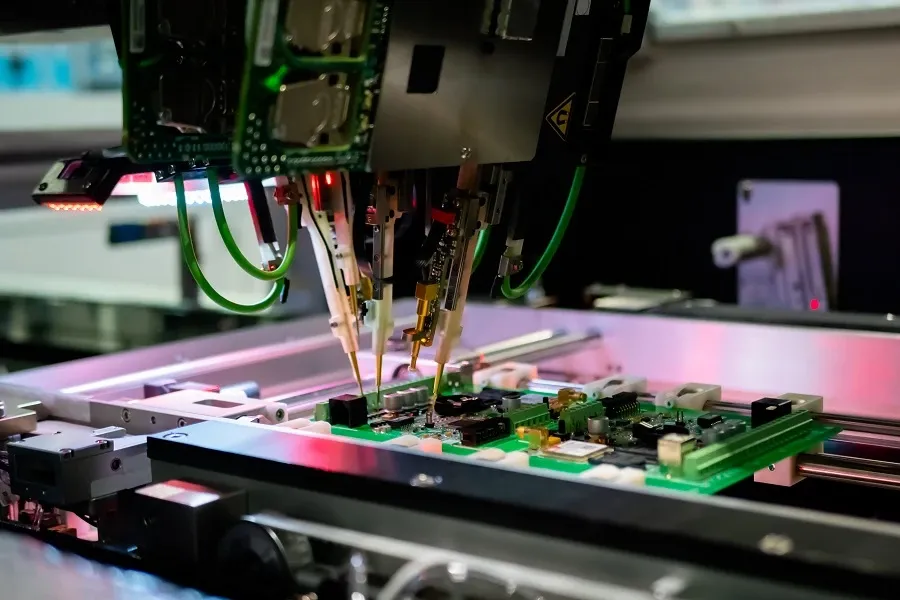
PCBWay offers comprehensive PCB assembly services, streamlining the transition from bare PCBs to fully populated boards. Their capabilities encompass component procurement, automated surface mount technology (SMT) assembly, and through-hole assembly, all supported by advanced automated assembly lines that ensure precision and efficiency.
The PCB assembly process at PCBWay is structured to provide a complete solution. It starts with careful component sourcing, where they can procure parts as specified by the customer or recommend alternatives based on availability and cost. This is followed by solder paste application on the bare PCB, high speed component placement using pick-and-place machines and reflow soldering process using specialized ovens to achieve permanent mounting of components.
For components that can not be mounted by pick and place machines, through-hole components are inserted manually and wave soldered, and for other more sensitive components, PCBWay offers manual soldering services too, ensuring that each PCB assembly meets the required functionality and electrical integrity requirements. Inspection by trained technicians is done at all stages of the assembly process ensuring that the finished board is ready to be used in the customer’s application.
- Component Procurement
PCBWay manages the sourcing of electronic components, ensuring authentic parts are used in the assembly process. They handle procurement from authorized distributors and can work with customer-supplied parts. - Surface Mount Technology (SMT)
The SMT process utilizes automated equipment for precise placement of surface mount components. This method allows for high-density and high-precision component mounting. - Through-Hole Assembly
PCBWay also provides through-hole assembly for components that cannot be surface-mounted, including manual insertion and soldering for certain parts, ensuring reliable connections for non-SMT components. - Automated Assembly Lines
The use of automated assembly lines enhances efficiency, reduces errors, and allows for faster turnaround times for both prototype and production volumes. - Quality Control Checks
Each assembly undergoes rigorous inspection and testing to ensure correct component placement, solder joint integrity, and overall board functionality.
Materials and Technologies Supported by PCBWay
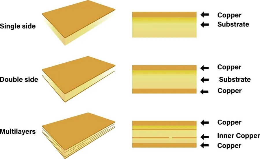
PCBWay provides a comprehensive range of materials and advanced technologies to meet diverse PCB design requirements. Their capabilities extend from standard substrates to specialized materials, and encompass cutting-edge manufacturing processes.
| Material | Description | Typical Applications | Key Properties |
|---|---|---|---|
| FR-4 | A common glass-reinforced epoxy laminate. It's versatile and cost-effective. | General-purpose PCBs, consumer electronics, prototyping | Good electrical insulation, flame retardant, moderate cost |
| Aluminum | Metal core PCB with an aluminum base. Excellent thermal conductivity. | LED lighting, power electronics, high-power devices | High thermal dissipation, durable |
| Flexible PCBs (Flex) | Polyamide or polyester based flexible substrates. Allows bending and folding. | Wearable devices, automotive sensors, aerospace applications | Flexible, lightweight, high density interconnection |
| High-Frequency Materials | Materials with controlled dielectric constant and low loss tangent. | RF and microwave circuits, high speed digital, antenna design | Low signal loss, stable dielectric properties at high frequency |
In addition to the diverse materials offered, PCBWay employs advanced manufacturing technologies such as:
- High-Density Interconnect (HDI)
HDI technology enables higher circuit density per unit area using microvias and fine lines, suitable for complex, space-constrained designs. - Advanced Surface Finishes
PCBWay offers multiple surface finishes like ENIG (Electroless Nickel Immersion Gold), HASL (Hot Air Solder Leveling), Immersion Tin, and OSP (Organic Solderability Preservative). Each finish provides specific benefits for solderability, corrosion protection and wire bonding. - Controlled Impedance
For high-speed digital and RF circuits, PCBWay can achieve controlled impedance traces using specific layer stacks and trace geometries to reduce signal reflections. - Blind and Buried Vias
These vias allow for complex layer interconnections without passing through the entire board, allowing high density designs and enhanced signal routing options.
Quality Assurance and Testing Procedures at PCBWay
PCBWay employs a comprehensive suite of quality assurance and testing procedures to ensure the delivery of high-quality printed circuit boards. This multifaceted approach includes rigorous design checks, functional testing, and adherence to stringent inspection standards, thereby minimizing defects and ensuring consistent performance.
- Design Rule Checks (DRC)
Prior to fabrication, PCBWay conducts thorough design rule checks. These automated checks verify that the design adheres to manufacturing constraints, including trace width, spacing, via sizes, and other critical parameters. This step minimizes the risk of fabrication errors and ensures the manufacturability of the design. - Automated Optical Inspection (AOI)
Following fabrication, each PCB undergoes Automated Optical Inspection (AOI). This non-contact inspection method uses high-resolution cameras to capture images of the PCB. The captured images are then compared against the design specifications to identify any discrepancies, such as shorts, opens, incorrect component placement, or solder issues. AOI is a critical step in defect detection before further processing. - In-Circuit Testing (ICT)
For assembled PCBs, PCBWay offers In-Circuit Testing (ICT). ICT involves using a bed-of-nails fixture to access and test individual components on the PCB. This allows for the identification of component-level failures, shorts, opens, and incorrect values, ensuring that the assembly is free of electrical defects. - Functional Testing
Functional testing is performed to verify that the assembled PCB functions as intended. It involves applying inputs and observing the outputs of the PCB according to the design specifications. This test helps ensure that the PCB is performing correctly in its intended application, identifying any design flaws or assembly issues. - X-Ray Inspection
For complex assemblies, such as those with Ball Grid Array (BGA) components, PCBWay utilizes X-ray inspection. This non-destructive testing method allows for visual inspection of internal connections and solder joints, identifying defects such as voids, solder bridges, or misalignments that cannot be seen with standard optical methods. X-ray inspection ensures the quality and reliability of complex assemblies. - Incoming Quality Control (IQC)
To ensure the quality of incoming materials, PCBWay performs Incoming Quality Control (IQC). This process involves verifying the specifications and quality of raw materials and components before being used in the manufacturing process, minimizing quality issues related to the starting materials. Component reels and trays are also inspected, and components verified to be accurate. - Final Visual Inspection
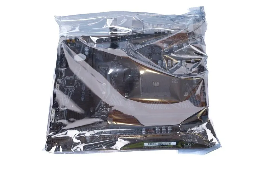
Before packaging and shipping, each PCB undergoes a final visual inspection. This manual inspection involves carefully examining the PCB for any physical defects or cosmetic issues, such as scratches, dents, or incorrect silkscreen printing. Final visual inspection ensures that only PCBs meeting the highest visual standards are shipped to customers.
PCBWay's Global Reach and Shipping Options
PCBWay has established a robust global presence, ensuring efficient PCB manufacturing and assembly services are accessible worldwide. Their streamlined logistics and diverse shipping options facilitate timely delivery, contributing to their position as a leader in the PCB industry.
PCBWay operates with a global supply chain, maintaining strategic partnerships with various logistics providers to ensure worldwide delivery. Their distribution network includes multiple shipping locations, optimizing delivery times and reducing costs for customers across different regions. This international infrastructure supports their capacity to handle both small-batch prototypes and large-scale production efficiently.
- Shipping Locations
PCBWay utilizes a network of shipping facilities strategically located across Asia, Europe, and North America. The precise shipping location may vary based on manufacturing site and order details, however, the user is not required to choose a specific location; PCBWay handles that process automatically based on efficiency, cost, and other supply chain considerations. - Shipping Partners
PCBWay partners with major international carriers such as DHL, FedEx, and UPS for delivery, ensuring tracking, accountability, and reliable delivery times. They also employ local carriers in specific regions for cost effectiveness and quicker delivery when appropriate. - Delivery Timeframes
Delivery timeframes vary depending on the customer's location, shipping method chosen, and production volume. Typical express delivery times range from 2 to 7 days, while standard options may take 7 to 20 days. PCBWay provides estimated delivery times at the time of order placement. The user should check on their order for the most accurate delivery time. - Customs and Duties
Customers are responsible for any applicable customs duties and taxes, which can vary significantly depending on the destination country. PCBWay provides necessary documentation to facilitate customs processing; however, the user should be aware of local regulations and expected import costs. - Order Tracking
PCBWay provides full tracking details to users with each order, enabling them to monitor the location of their shipment. This transparency ensures clear communication and helps users plan accordingly.
The speed of PCBWay's global logistics is a critical advantage. Their ability to deliver quickly and reliably is essential, especially for prototyping where design iterations and changes are frequent, and for production where time to market is critical. This combination of broad accessibility, speed and quality makes PCBWay an efficient choice for PCB manufacturing and assembly worldwide.
Frequently Asked Questions About PCBWay
This section addresses common inquiries about PCBWay, providing clear and concise answers regarding their services, operations, and processes to enhance user understanding and confidence in their offerings.
- What exactly does PCBWay do?
PCBWay is a comprehensive PCB (Printed Circuit Board) manufacturing and assembly service provider. They offer a range of services, including PCB prototyping, small to large batch production, and complete PCB assembly, catering to diverse project needs from individual makers to large-scale industrial clients. They also offer services such as stencil production. - Where does PCBWay ship its products from?
PCBWay primarily ships from its manufacturing facilities located in China. However, they utilize global logistics networks to ensure worldwide delivery to their customers. The specific shipping location may vary depending on the order size and destination. - Where is PCBWay's main company location?
PCBWay is headquartered in Hangzhou, China. This location serves as the central hub for their operations, including manufacturing, customer service, and research and development. They have additional locations to support global sales and logistics. - How long does PCBWay typically take to review a PCB design?
The PCB design review process at PCBWay is generally quite efficient. Typically, a standard review takes between a few hours to 24 hours. More complex designs may require additional review time. They will provide a quotation and advise on any design issues promptly after review. - What types of PCB materials does PCBWay support?
PCBWay supports a wide array of materials, including the standard FR-4, aluminum-backed PCBs for thermal management, flexible PCBs for non-rigid applications, and high-frequency materials like Rogers for specialized RF applications. This material diversity provides options for various applications and performance needs. - Does PCBWay offer PCB Assembly services?
Yes, PCBWay provides comprehensive PCB assembly services. This includes component procurement, SMT (Surface Mount Technology) assembly, through-hole assembly, and final testing. They offer both partial and full turnkey assembly options. This makes PCBWay a one-stop solution for PCB fabrication and assembly, eliminating supply chain complexities. - What are PCBWay's options for surface finish?
PCBWay offers a wide array of surface finishes including HASL (Hot Air Solder Leveling), ENIG (Electroless Nickel Immersion Gold), Immersion Tin, Immersion Silver, and OSP (Organic Solderability Preservative). The choice of finish depends on your application needs, cost considerations, and desired solderability and longevity.
Comparing PCBWay with Other PCB Manufacturers
Choosing the right PCB manufacturer is critical for the success of any electronics project. This section provides a comparative analysis of PCBWay against other major players in the PCB manufacturing industry, focusing on key factors such as price, quality, and delivery times to aid in making informed decisions.
| Feature | PCBWay | Competitor A | Competitor B | Competitor C |
|---|---|---|---|---|
| Price (for Prototype) | Competitive | Higher | Moderate | Higher |
| Price (for Mass Production) | Competitive | Higher | Moderate | Higher |
| Quality (Based on User Reviews) | High | High | Moderate | High |
| Delivery Time (for Prototypes) | Fast | Moderate | Slow | Fast |
| Delivery Time (for Mass Production) | Fast | Moderate | Slow | Moderate |
| Supported Materials | Wide Range | Limited | Moderate | Wide Range |
| Assembly Capabilities | Comprehensive | Basic | Moderate | Comprehensive |
| Customer Support | Responsive | Moderate | Slow | Responsive |
| Online Quote and Ordering Platform | User-Friendly | Complex | Moderate | User-Friendly |
How to Get Started with PCBWay
Initiating a PCB manufacturing or assembly project with PCBWay is a streamlined process designed for both novice and experienced users. This section provides a step-by-step guide to ensure a smooth ordering experience, covering critical aspects from file preparation to final order placement.
- Prepare Your PCB Design Files
Ensure your design files are in Gerber format (RS-274X is recommended) along with any necessary drill files (Excellon format). Include a bill of materials (BOM) in CSV or Excel format for assembly projects, specifying component part numbers, manufacturers, and quantities. Verify that your CAD software's output settings are correct to avoid common design interpretation issues. Always double check your design files for errors before submission. For assembly, also make sure to provide component placement (centroid) files. - Obtain an Instant Quote
Visit the PCBWay website and upload your Gerber files. The online platform will analyze your design and provide an instant quote based on your specified parameters, such as board dimensions, layer count, material type, and quantity. For assembly projects, you'll need to upload your BOM and placement files for an accurate quote. Utilize their platform's capabilities to adjust specifications and observe how they impact pricing, allowing you to optimize your project budget. - Specify Manufacturing and Assembly Options
Review the quote and select your preferred manufacturing options, such as PCB finish (e.g., HASL, ENIG), solder mask color, and silk screen requirements. For assembly projects, select your assembly options like SMT, through-hole, or mixed assembly. Ensure that the components you specified are within PCBWay's sourcing capabilities, if you're not providing the components yourself. Confirm all options are aligned with your design and project goals. - Perform Design Rule Checks (DRC)
Prior to submitting your order, run a Design Rule Check (DRC) on your Gerber files using PCBWay's online tool or your CAD software. This step is critical for identifying potential manufacturability issues such as trace widths, spacing, via sizes, and other parameters. Resolving these issues early can prevent costly delays and ensure your PCBs are produced as intended. PCBWay also has a team that will help flag issues that are discovered. - Place Your Order and Make Payment
After reviewing the quote, confirming the options, and passing the DRC, you can proceed to place your order. Select your preferred payment method, and provide all necessary shipping details. Upon completion, you will receive an order confirmation and start the production process. PCBWay also provides order tracking during the whole process. - Monitor Production and Shipping
You will receive updates on the production status of your PCBs. After completion, your order will be shipped and you will receive tracking information, ensuring you are informed through the whole process.
Following these steps will streamline your experience with PCBWay, and ensure a smooth transition from design to physical boards and assembled products. Their online platform and customer support team are designed to help users navigate through the process, providing assistance and resources as needed.
PCBWay has established itself as a reliable partner for engineers and designers around the globe, providing a one-stop solution for PCB manufacturing and assembly. From prototyping to full production, their services are geared toward supporting innovation and bringing ideas to life with high quality and efficiency. PCBWay's commitment to quality, coupled with its advanced manufacturing capabilities, positions it as a leading player in the PCB industry, continuously shaping how we interact with technology. As PCB technologies evolve, PCBWay is poised to continue providing cutting-edge solutions, further enabling the next generation of electronic devices and innovations.