Revolutionizing Electronics: 3D Printed Circuit Boards Explained
From intricate smart devices to complex industrial machinery, electronics are at the core of our modern world, and their manufacturing relies heavily on circuit boards. Now, a new technology is emerging to change the way we design and create these critical components: 3D printed circuit boards. This article will explore how this innovative approach works, offering a detailed overview of its advantages, challenges, and the potential for the future.
What is a 3D Printed Circuit Board?
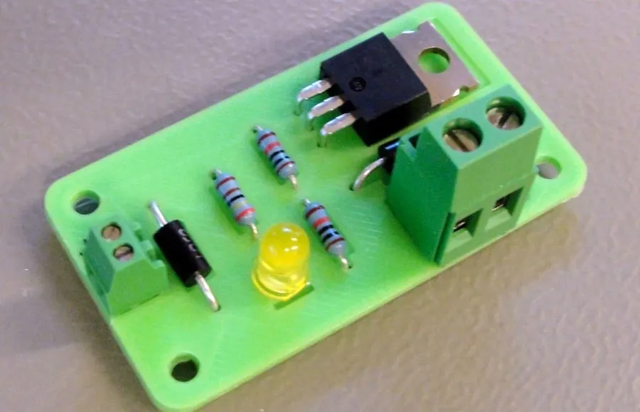
A 3D printed circuit board is an electronic circuit fabricated using additive manufacturing techniques, where conductive materials are deposited layer by layer to form the desired traces, vias, and other circuit features, offering an alternative to traditional subtractive PCB manufacturing methods.
Unlike conventional PCBs, which are typically etched from a copper-clad laminate, 3D printed PCBs allow for the creation of circuits on complex, non-planar substrates, and offer the potential to integrate the board directly into the final product structure. Common 3D printing technologies for PCBs include material extrusion with conductive inks or pastes, inkjet printing with nanoparticle conductive materials, and stereolithography with specialized conductive resins.
The materials utilized in 3D printed PCBs vary, encompassing polymers for the base substrate and conductive inks or pastes containing metals such as silver or copper. These conductive materials are crucial in defining the performance and reliability of the circuit. 3D printed circuit boards are gaining traction for applications that require rapid prototyping, custom designs, and the integration of electronics into unconventional geometries.
3D Printing Methods for Circuit Boards

The creation of 3D printed circuit boards leverages various additive manufacturing techniques, each with unique capabilities in terms of precision, material compatibility, and cost. These methods are crucial for translating digital designs into functional electronic circuits. This section details several prominent 3D printing methods used for circuit board fabrication, emphasizing their specific processes and implications for performance and cost.
A detailed look at the technology of various 3D printing methods for circuit boards:
- Fused Deposition Modeling (FDM)
FDM, a widely used 3D printing method, involves extruding a thermoplastic filament through a heated nozzle, creating the board layer by layer. In PCB fabrication, conductive filaments are used for the circuit traces, along with standard non-conductive filaments for the substrate. While cost-effective, FDM's layer resolution might limit its use for intricate circuit designs. - Inkjet Printing
Inkjet printing deposits conductive inks onto a substrate, creating circuit traces. This method enables precise material deposition and is suitable for complex designs. The nature of the material used in the ink can impact trace performance and cost, with specialized inks often being expensive. This makes inkjet printing ideal for prototyping and low-volume production, but high-volume production can be expensive. - Material Extrusion
Material extrusion involves dispensing conductive pastes or inks through a nozzle, allowing for the direct creation of conductive pathways on a substrate. This method offers the potential to use a wide range of materials, however, the method’s precision and consistency can vary, depending on equipment and material properties. - Aerosol Jet Printing
Aerosol jet printing uses a fine mist of conductive material which is then deposited onto a substrate. This method is particularly good at printing on a wide variety of substrates and curved surfaces, and can achieve very fine trace widths. Its advantages are offset by relatively higher equipment costs.
The choice of printing method significantly impacts the final cost, accuracy, and material versatility of the 3D printed PCB. Each approach presents its unique advantages and disadvantages. The selection should be based on the specific application requirements and the trade-offs that are acceptable. For example, the FDM method is cost effective, but limited by precision, while Inkjet printing can produce fine traces, but specialized inks can be more expensive. Understanding the nuances of each method is crucial for choosing the optimal path for PCB fabrication.
Benefits of Using 3D Printed PCBs
3D printed PCBs offer a compelling alternative to traditional manufacturing methods, providing significant advantages in rapid prototyping, design flexibility, and cost efficiency, especially for specialized applications. These benefits stem from the additive manufacturing process, which allows for creating intricate geometries and integrating electronics directly into enclosures.
- Rapid Prototyping
3D printing significantly accelerates the prototyping process by eliminating the need for tooling or masks, allowing engineers to quickly iterate through designs and test them in real-world conditions. - Customization for Complex Designs
The additive nature of 3D printing facilitates the creation of complex and unique shapes, curved surfaces, and embedded features that are difficult or impossible to achieve with traditional subtractive PCB manufacturing techniques. This includes conformal electronics and non-planar circuit boards. - Reduced Manufacturing Time
3D printing reduces lead times from weeks to days or even hours. This efficiency allows for a much faster product development cycle by quickly producing a small batch of circuit boards. - Cost Reduction for Small Batches
For small quantities or highly customized circuit boards, 3D printing is often more economical compared to traditional methods, which incur significant setup costs. It enables just-in-time manufacturing and reduces inventory waste. - Direct Integration of Electronics
3D printing enables the direct integration of electronic components into the structural or functional enclosure, simplifying design, reducing assembly, and overall system weight and size. This is particularly useful in applications with space constraints.
Limitations and Challenges of 3D Printed PCBs

While 3D printed PCBs offer exciting possibilities, several limitations and challenges hinder their widespread adoption. These hurdles primarily revolve around material properties, manufacturing precision, scalability, and cost-effectiveness. Addressing these is crucial for the technology to reach its full potential.
- Material Limitations
Currently, the range of materials suitable for 3D printing conductive traces and substrates is limited. Many printable materials exhibit lower conductivity compared to traditional PCB materials like copper, leading to performance trade-offs. Further, the thermal properties and mechanical strength of printable materials can also be constraints for some applications. - Layer Resolution and Precision
Achieving high-resolution traces and precise layer alignment with 3D printing is challenging. Compared to traditional photolithography processes, current 3D printing methods often struggle with fine detail, limiting the density and complexity of circuits that can be printed. This can impact signal integrity, especially in high-frequency applications. - Conductive Trace Quality and Resistance
The conductive traces produced by 3D printing methods may not always achieve the same quality and conductivity as those created through traditional etching or plating processes. Higher resistance in 3D printed traces can result in increased power losses, heat generation, and ultimately, reduced efficiency, which is critical for electronic performance. - Scalability for Mass Production
Current 3D printing technologies are primarily geared towards prototyping and low-volume production. Scaling up for mass production faces hurdles in terms of printing speed, accuracy, and consistency. The time taken to print a single board is far longer than that using traditional methods, making mass production less economical - Cost of Specialty 3D Printing Systems
Specialized 3D printers capable of handling conductive inks and materials needed for PCB printing are typically more expensive than standard 3D printers. This high initial investment can deter smaller companies and research institutions from adopting this technology, especially when mass production is not yet feasible.
3D Printed Circuit Board Applications

3D printed circuit boards are rapidly expanding beyond experimental stages, finding practical applications in various sectors where traditional PCB manufacturing faces limitations. These applications leverage the unique capabilities of 3D printing, such as rapid prototyping, custom design flexibility, and the ability to integrate electronics within non-planar structures.
- Rapid Prototyping
The foremost application is in rapid prototyping. 3D printing allows engineers to iterate quickly on designs, testing new concepts and making modifications without the delays and costs associated with traditional PCB fabrication. This speed and flexibility significantly accelerate the development cycle for electronic products. - Custom Electronics
Custom electronics design is greatly facilitated by 3D printing. Complex shapes and unique form factors for printed circuit boards that are difficult or impossible with traditional methods become feasible. This empowers designers to create highly specialized and optimized electronic systems for specific applications. - Aerospace
The aerospace industry benefits from 3D printed circuit boards due to their potential for lightweighting, customized form factors, and the ability to withstand harsh environments. Components with integrated electronics can be directly fabricated, reducing assembly steps and improving reliability. - Medical Devices
In the medical field, 3D printed PCBs are used for producing customized wearable sensors, implants, and diagnostic tools. The ability to create patient-specific devices is invaluable, especially in fields like prosthetics and personalized healthcare solutions. - Niche Industries
Beyond these sectors, various niche industries benefit significantly, including research laboratories needing specialized test equipment, artists exploring interactive installations, and educational institutions developing innovative teaching tools. These examples highlight how 3D printing fills the gaps where conventional PCB production falls short.
Case studies further illustrate the impact of 3D printed circuit boards. For instance, a recent study detailed the use of 3D printed flexible PCBs for custom wearable health monitoring devices that were impossible to create with traditional methods. This study demonstrated a marked reduction in production costs and time, alongside higher performance than previously achieved. Another example is the use of 3D printed PCBs in CubeSats (miniature satellites), where custom-designed circuit boards were integrated directly into the structural components of the satellite, reducing weight and volume significantly. Such case studies underline the potential of 3D printed PCBs in creating innovative products for specialized requirements.
Frequently Asked Questions About 3D Printed Circuit Boards
This section addresses common questions about 3D printed circuit boards, providing clear and concise answers to help you understand this emerging technology.
- Is it possible to 3D print a circuit board?
Yes, it is indeed possible to 3D print circuit boards. Specialized 3D printing techniques and conductive materials allow for the creation of functional electronic circuits layer by layer. This differs from traditional manufacturing which uses etching and subtractive processes. - What is the difference between PCB and PWB?
While often used interchangeably, PCB (Printed Circuit Board) typically refers to the board with electronic components attached, whereas PWB (Printed Wiring Board) refers to the base board itself, without any components. However, in most contexts, the terms are used synonymously. - Are there limitations on what can be 3D printed?
While 3D printing offers great versatility, certain restrictions apply. Intellectual property rights related to designs or products should be respected, and printing items that are illegal or regulated is prohibited. Users need to be aware of the legal and ethical implications. - How many layers can a 3D printed circuit board have?
The number of layers in a 3D printed circuit board depends on the printing technology and materials used. While simpler boards might be single or double-layered, advanced 3D printing methods can create multi-layered boards, though they typically do not reach the layer counts achievable in traditional PCBs. - What materials are used to 3D print circuit boards?
3D printed circuit boards use a variety of materials including conductive inks or polymers, non-conductive substrate materials, and support materials. The choice depends on factors like conductivity, mechanical strength, and temperature resistance. - How does the cost of 3D printed PCBs compare to traditional PCBs?
The cost of 3D printed PCBs varies. For prototyping and small-batch production, it can be cost-effective due to reduced setup costs and rapid iteration. However, for large-scale production, traditional PCB manufacturing is usually more economical due to economies of scale. - What level of conductivity can be achieved with 3D printed traces?
The conductivity of 3D printed traces can vary significantly depending on the conductive material and printing process. While not as conductive as copper traces in traditional PCBs, significant advancements are continually being made to improve the conductivity of 3D printed materials.
Comparing 3D Printed PCBs vs Traditional PCBs
While 3D printed circuit boards offer innovative solutions for rapid prototyping and customized designs, traditional printed circuit boards (PCBs) remain the industry standard for mass production due to their established processes and reliable performance. This section provides a comparative analysis between these two technologies.
| Feature | 3D Printed PCBs | Traditional PCBs |
|---|---|---|
| Materials | Primarily conductive polymers, composites, and specialized inks. Limited range of materials. | Typically FR-4 (fiberglass epoxy), copper, and solder mask. Wide range of materials available. |
| Manufacturing Time | Faster for prototypes and custom designs; slower for large batches. | Longer for prototypes, but highly efficient for mass production. |
| Cost | Potentially lower for low-volume, custom projects; higher for mass production. | Lower for mass production, but higher for custom prototypes. |
| Design Complexity | Highly versatile, enabling complex geometries and integrated enclosures. Complex multi-layer structures can be challenging. | Standard planar designs with limitations on shape and integrated features. |
| Layer Resolution | Limited by printing resolution; achieving fine traces and high density remains a challenge. | High resolution, supports very fine traces and high-density interconnections. |
| Conductive Trace Quality | Conductivity and resistance can vary; conductive trace quality is generally lower than traditional PCBs. | Highly reliable with excellent conductivity and low resistance. |
| Mass Production | Challenging; current technologies are not well-suited for high-volume manufacturing. | Established and highly optimized for large-scale production. |
| Performance | Performance can be limited by materials and trace conductivity; suitable for low to mid range applications. | High performance and reliability; suitable for high-performance applications. |
| Customization | Excellent for highly customized designs and unique shapes; allows integration with enclosures. | Limited to standard shapes and sizes, minimal customization capabilities |
| Environmental Impact | Potentially less waste due to additive manufacturing, but material sourcing can be impactful. | Potentially more waste from subtractive manufacturing (etching) but has recycling solutions. |
The Future of 3D Printed Circuit Boards
The trajectory of 3D printed circuit boards points towards a significant transformation in electronics manufacturing, driven by technological advancements and the evolving demands of the industry. This section explores the potential of 3D printing in the future of electronics manufacturing, and its impact on global supply chains and prototyping.
- Technological Advancements
Anticipated improvements include enhanced material properties, higher resolution printing capabilities, and the ability to integrate more complex electronic components directly during the printing process. Research into new conductive inks and printable substrates is crucial for overcoming current limitations in conductivity and material performance. These advancements will allow for more functional and reliable 3D printed PCBs. - Emerging Markets
As the technology matures, new markets are expected to emerge, especially in areas requiring customized electronics, rapid prototyping, and low-volume production. This includes applications in aerospace, medical devices, wearables, and customized industrial equipment. The ability to quickly iterate on designs and produce them on-demand will be a key factor in the growth of these markets. - Impact on Global Supply Chains
The advent of 3D printed PCBs has the potential to decentralize manufacturing, reducing dependence on traditional, centralized production facilities. This shift could lead to more resilient supply chains, less reliance on long lead times, and reduced transportation costs. Localized manufacturing will become more feasible for electronics, with companies printing their custom circuits on-demand, potentially reducing geopolitical supply chain risks and bolstering self-sufficiency. - Rapid Electronics Prototyping
The ability to quickly translate designs into physical prototypes is a substantial benefit, reducing product development times. This capability facilitates iterative design processes with rapid modifications, accelerating the path from concept to market. 3D printing will allow engineers to quickly prototype and validate new ideas, leading to more innovative and agile product development cycles. - Integration of Electronics
Future trends also suggest a closer integration of electronics within the structural components of products. With advanced 3D printing, it will be possible to embed circuit traces directly into the mechanical parts of devices, which will lead to lighter, more compact, and more efficient electronic systems. This will not only optimize space utilization but also enable the creation of novel product architectures.
3D printed circuit boards represent a significant leap in electronics manufacturing, offering enhanced flexibility and customization. While still facing challenges, the technology's continued development holds immense promise for transforming how we design, manufacture, and integrate electronic components, paving the way for a new era of rapid prototyping and unique design capabilities. Embracing the potential of 3D printed circuit board can revolutionize how we build the future's most innovative technology.