RF Board: Understanding, Design, and Applications of Radio Frequency PCBs
In our increasingly wireless world, radio frequency (RF) technology permeates our lives, from smartphones to satellite communication. At the heart of many RF devices lies the RF board, a specialized printed circuit board (PCB) designed to handle high-frequency signals effectively. These boards are more than just a substrate for components; they are engineered to ensure signal integrity, minimize losses, and support complex modulation schemes. This article delves into the fascinating world of RF PCBs, exploring their unique characteristics, design principles, manufacturing challenges, and diverse applications, from consumer electronics to high-end aerospace equipment, making these boards the unsung heroes of our interconnected life.
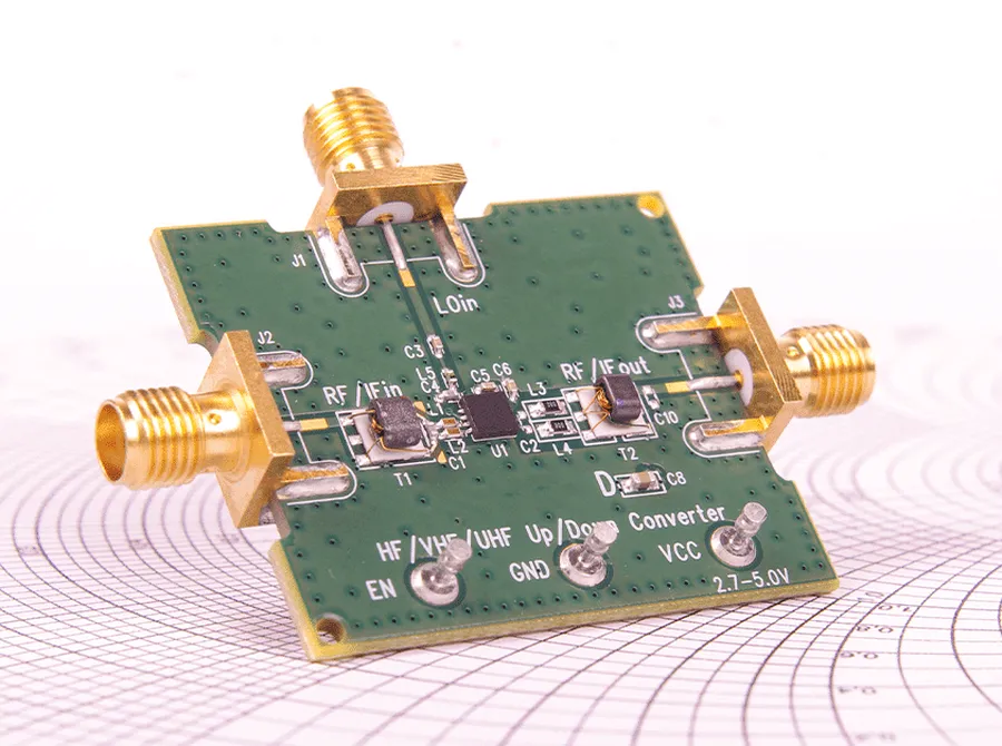
What is an RF Board?
An RF board, or Radio Frequency Printed Circuit Board (PCB), is a specialized type of PCB engineered to operate effectively within the radio frequency spectrum. Unlike standard PCBs designed for low-frequency signals, RF boards are optimized to minimize signal loss, maintain impedance control, and reduce electromagnetic interference (EMI), which are crucial for reliable performance at high frequencies. These boards are fundamental in various applications from telecommunications to aerospace, where the transmission and reception of radio waves are paramount.
Key Differences Between RF PCBs and Standard PCBs
RF PCBs are specifically engineered for high-frequency applications, differing significantly from standard PCBs in materials, design, and manufacturing. These distinctions are crucial for managing impedance, minimizing signal loss, and controlling thermal characteristics, all of which are paramount at radio frequencies.
| Feature | Standard PCB | RF PCB |
|---|---|---|
| Primary Application | General-purpose electronics | High-frequency signal processing |
| Material | Primarily FR-4 | Specialized materials like PTFE, ceramics, or low-loss FR-4 variants |
| Impedance Control | Less critical, often not tightly controlled | Highly critical; precise impedance matching required (e.g., 50Ω, 75Ω) |
| Signal Loss | Higher loss at high frequencies | Minimized signal loss through low-loss materials and design |
| Thermal Management | Moderate thermal management needs | Greater emphasis on heat dissipation due to higher operating frequencies |
| Design Considerations | Standard trace routing, less focus on high frequency effects | Strict trace width and spacing control, use of controlled impedance traces, minimal vias, and grounding techniques |
| Manufacturing Process | Standard manufacturing processes | Tighter tolerances, precise etching, controlled depth drilling, and special plating techniques |
The selection of materials for RF PCBs is deliberate, often utilizing substrates with low dielectric loss to minimize signal attenuation. Design considerations are crucial, incorporating impedance-controlled traces and minimizing discontinuities. Manufacturing of RF PCBs requires more precise fabrication techniques than standard PCBs to ensure the reliability and performance of the board in high frequency applications.
Materials Used in RF Board Fabrication
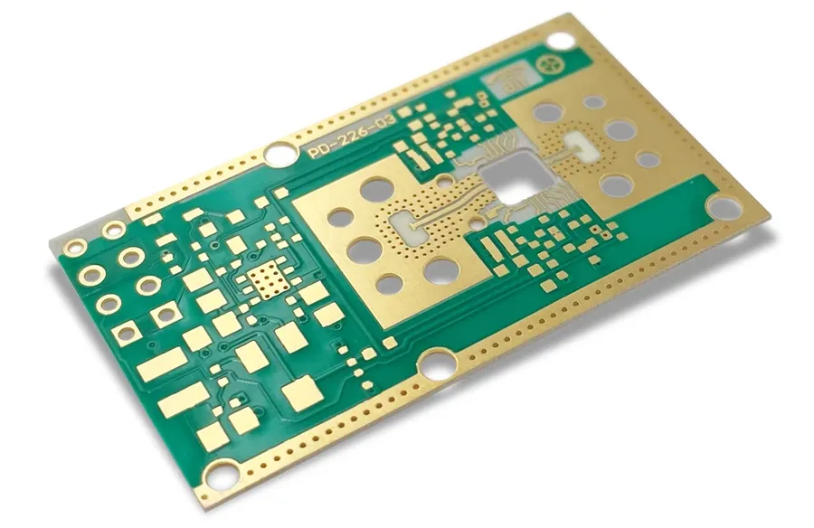
The selection of substrate materials in RF PCB fabrication is paramount to achieving optimal performance at high frequencies. These materials dictate the electrical, thermal, and mechanical characteristics of the board, significantly influencing signal integrity, power efficiency, and overall reliability. Key material properties include dielectric constant, loss tangent, and thermal conductivity, which are meticulously considered based on the specific application requirements.
| Material | Dielectric Constant (εr) | Loss Tangent (tan δ) | Thermal Conductivity (W/m·K) | Typical Applications | Advantages | Disadvantages |
|---|---|---|---|---|---|---|
| FR-4 | 4.3-4.7 | 0.020 | 0.2-0.3 | Low-frequency RF, general purpose | Cost-effective, widely available, good mechanical strength | High losses at high frequencies, not suitable for high-performance RF applications. |
| PTFE (Teflon) | 2.1-3.5 | 0.0002-0.002 | 0.25 | High-frequency RF, microwave applications | Low dielectric loss, excellent high-frequency performance, good temperature stability | More expensive, mechanically softer than FR-4, may require special processing. |
| Ceramic | 6-10 | 0.0001-0.001 | 20-30 | High power RF, high temperature applications | Excellent high-frequency performance, very low loss, high thermal conductivity, excellent stability | Expensive, brittle, difficult to process. |
| Rogers 4350B | 3.66 | 0.0037 | 0.62 | High frequency applications | Good mechanical strength and low electrical loss, excellent dimensional stability | More expensive than FR-4 |
| Rogers 4003C | 3.55 | 0.0027 | 0.71 | High frequency applications | Low loss, stable dielectric constant, good dimensional stability. | More expensive than FR-4 |
Essential Design Considerations for RF PCBs
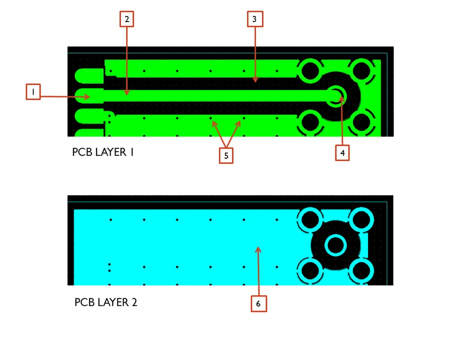
Designing RF PCBs requires meticulous attention to detail due to the high-frequency signals involved. Key considerations include impedance control, trace layout, via design, grounding strategies, and shielding to ensure minimal signal loss and interference, which are paramount for optimal performance. These aspects differ significantly from standard PCB design, emphasizing precision and a deep understanding of electromagnetic principles.
- Impedance Matching
Achieving impedance matching is crucial to prevent signal reflections and ensure maximum power transfer. This involves precisely controlling trace widths and spacing to match the characteristic impedance of the transmission line, typically 50 ohms for many RF applications. Discontinuities in impedance can lead to signal degradation and power loss. - Trace Width and Spacing
Trace dimensions (width and spacing) directly impact impedance and signal integrity. RF traces must be carefully calculated and implemented to maintain consistent impedance and minimize signal losses. Moreover, spacing between traces and nearby copper areas affects signal coupling and must be well-managed to avoid interference. Generally, a wider trace leads to lower impedance and vice versa. - Via Design
Vias, used to connect different layers in a PCB, can cause impedance discontinuities at high frequencies if not carefully designed. Their parasitic inductance and capacitance must be minimized through the use of via stitching, via-in-pad techniques, and careful placement to ensure seamless signal transitions between layers. Optimizing via design can reduce signal degradation and signal reflection. - Grounding Techniques
Effective grounding is essential for reducing noise and improving signal integrity. Employing a solid ground plane, multiple ground vias, and proper grounding connections can create a low-impedance return path for RF signals, minimizing ground bounce and electromagnetic interference (EMI). Star grounding or multiple return paths are recommended to achieve low return impedance, especially in mixed-signal PCBs. - Shielding
Shielding is often necessary to prevent electromagnetic interference (EMI) from affecting sensitive RF circuits or from radiating outwards and causing interference with other devices. Techniques include using conductive enclosures, metalized walls, grounded shielding cans, and careful component placement. Proper shielding can greatly enhance the performance and reliability of RF systems. - Role of PCB Design Software
Specialized PCB design software, equipped with RF design capabilities, is crucial for successful RF PCB development. These software tools help in simulating and optimizing signal paths, calculating trace impedance, performing electromagnetic simulations, and ensuring adherence to design rules. Features like 3D visualization and signal integrity analysis enable engineers to effectively design and validate their circuits before the manufacturing stage.
| Design Parameter | Impact on RF Performance | Typical Design Consideration |
|---|---|---|
| Impedance Matching | Minimizes signal reflection, maximizes power transfer | Use of controlled impedance traces; impedance calculators |
| Trace Width and Spacing | Affects impedance, signal integrity, and coupling | Careful calculation based on required impedance; minimum spacing rules. |
| Via Design | Can introduce impedance discontinuities and signal loss | Minimize via count; via stitching; via-in-pad |
| Grounding Techniques | Reduces noise, improves signal integrity, provides return path | Solid ground plane, multiple ground vias, star grounding |
| Shielding | Prevents EMI, enhances signal isolation | Use of conductive enclosures, metalized walls, shielding cans |
RF PCB Manufacturing Processes
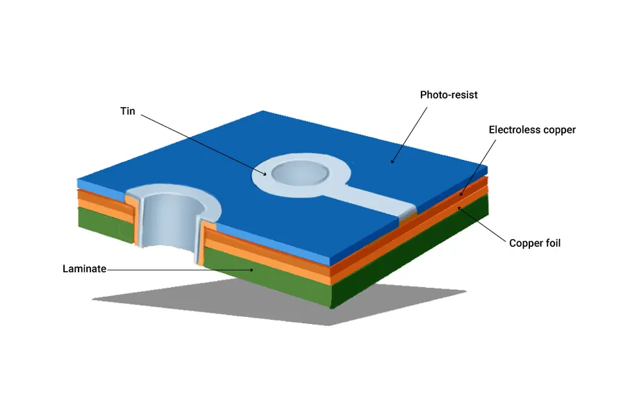
The manufacturing of RF PCBs necessitates a higher degree of precision and control compared to standard PCBs due to the delicate nature of radio frequency signals. Key processes such as etching, drilling, plating, and quality control are refined to meet the stringent performance requirements of high-frequency applications, emphasizing the importance of maintaining tight tolerances throughout the fabrication.
- Etching Precision
Achieving precise trace widths and spacing is paramount for impedance control in RF circuits. Chemical etching processes are carefully monitored to ensure minimal variations and sharp edges, which directly impact signal integrity. Advanced etching techniques, such as photo-chemical machining, are often employed to meet these demands. - Controlled Depth Drilling
RF PCBs often require blind and buried vias to optimize signal routing and minimize parasitic effects. Controlled depth drilling techniques are utilized to precisely create vias at specific depths, avoiding unnecessary signal reflections and maintaining impedance consistency. Laser drilling is favored for its accuracy and minimal thermal impact. - Plating Techniques
Uniform plating is critical for RF performance. Consistent metal plating thickness is essential for proper impedance matching and minimizing signal attenuation. Specialized plating methods, such as electrolytic and electroless plating, are used to achieve the required uniformity and conductivity. Immersion plating is preferred for its superior solderability and corrosion resistance. - Quality Control Measures
Rigorous testing and inspection processes are integral to the manufacturing of RF PCBs. These include electrical testing (impedance testing, signal integrity analysis), dimensional inspections, and microscopic evaluations to detect any defects. Automated optical inspection (AOI) and X-ray inspection techniques are frequently used to ensure the highest quality standards and adherence to specifications. - Importance of Tight Tolerances
Maintaining tight dimensional tolerances is crucial in RF PCB manufacturing, especially considering high-frequency signal wavelengths are often very small. Deviations in trace width, spacing, and layer alignment can cause impedance mismatches and signal losses. Advanced manufacturing and measurement techniques ensure that the final product meets all required design specifications.
RF Board Applications Across Industries
RF boards, with their capacity to handle high-frequency signals, are indispensable across numerous industries. Their specialized design and material properties make them a crucial component in enabling wireless communication, radar technology, and high-speed data processing.
- Telecommunications
RF PCBs are fundamental in both 4G and 5G infrastructure, facilitating signal transmission and reception in base stations, mobile devices, and network equipment. These boards ensure efficient signal propagation and minimal loss, vital for high-speed data transfer. - Aerospace and Defense
In aerospace, RF boards are used in satellites, drones, and radar systems. Their robust design ensures reliable performance under extreme environmental conditions, and their high precision is critical for maintaining system accuracy in navigation and communication. - Automotive
RF boards play a significant role in Advanced Driver-Assistance Systems (ADAS). They support features such as radar for collision avoidance, vehicle-to-vehicle communication, and GPS navigation, withstanding harsh conditions in automotive applications. - Medical Devices
Medical imaging equipment, including MRI and ultrasound machines, rely on RF boards for precise and clear signal processing. The low-noise characteristics of these boards are crucial for capturing accurate diagnostic information, ensuring patient safety and effective treatment. - Internet of Things (IoT)
Many IoT devices use RF boards to connect to networks, enabling data transfer in smart home applications, industrial monitoring systems, and wearable technology. Their compact form factor allows seamless integration into a variety of small, connected devices. - Consumer Electronics
Wireless consumer products like smartphones, laptops, tablets, and wearable devices incorporate RF boards for Wi-Fi, Bluetooth, and other wireless communication technologies. These boards are optimized for low power consumption and high data rates, enhancing user experiences. - Radar Systems
RF boards are the backbone of radar systems across various domains, including weather forecasting, air traffic control, and military applications. The performance of these systems critically depends on the high-frequency handling capabilities of RF PCBs.
| Industry | Application | Key RF Board Requirements |
|---|---|---|
| Telecommunications | Base stations, mobile devices | High-frequency signal handling, low signal loss |
| Aerospace | Satellites, drones, radar systems | Robust design, high precision, environmental resilience |
| Automotive | ADAS, radar, communication systems | Durability, reliability, high-speed data transfer |
| Medical Devices | MRI, ultrasound, imaging equipment | Low noise, high precision, clear signal processing |
| IoT | Smart home devices, industrial sensors | Compact size, low power consumption, reliable connectivity |
| Consumer Electronics | Smartphones, laptops, wearables | Low power consumption, high data rates, compact design |
| Radar Systems | Weather forecasting, air traffic control, military applications | High-frequency handling, signal integrity, accuracy |
Troubleshooting Common Issues in RF Boards
RF boards, while essential for high-frequency applications, are susceptible to a range of issues that can compromise their performance. Effective troubleshooting requires a systematic approach that combines an understanding of RF principles with practical measurement techniques. Common problems include impedance mismatch, signal loss, excessive noise, and thermal hotspots.
- Impedance Mismatch
Impedance mismatch occurs when the characteristic impedance of the transmission line does not match the source or load impedance, leading to signal reflections and power loss. This can be diagnosed using a vector network analyzer (VNA) to measure the return loss or VSWR (Voltage Standing Wave Ratio). Solutions often involve adjusting trace widths, spacing, or adding impedance matching networks. - Signal Loss
Signal loss, or attenuation, increases with frequency and trace length. It can be caused by dielectric losses, skin effect, and radiation. Analyzing the S-parameters of the circuit with a VNA will quantify the signal loss. Employing low-loss materials, reducing trace length, and ensuring proper shielding will help mitigate signal loss. - Noise
Noise in RF circuits can originate from various sources including external interference, component noise, and poor grounding. Identifying the source using spectrum analyzer and proper shielding methods. Implementing good grounding practices, filtering, and shielding techniques helps reduce noise and unwanted signal coupling. - Thermal Issues
Thermal issues arise due to power dissipation in components, leading to performance degradation and potential failure. Thermal imaging can reveal hotspots, and a detailed thermal analysis can be performed using simulations. Heat sinks, improved thermal management techniques, and efficient component placement can help manage thermal challenges.
Diagnostic tools such as Vector Network Analyzers (VNAs), Spectrum Analyzers, and Thermal Cameras are indispensable for troubleshooting RF boards. Furthermore, meticulous visual inspection using magnification can expose manufacturing defects or damage. Corrective actions may involve PCB rework, circuit adjustments, or component replacements. Consistent and thorough testing at each stage is essential to guarantee reliable performance.
Frequently Asked Questions About RF Boards
This section addresses common questions about RF boards, providing clear and concise answers to help clarify their function and use in various applications.
- What exactly are RF boards?
RF boards, or Radio Frequency boards, are specialized printed circuit boards designed to operate effectively at high frequencies. Unlike standard PCBs, they are optimized to handle radio frequency signals with minimal signal loss and interference, which is crucial in applications involving wireless communications. - What does 'RF' mean in electrical engineering?
In electrical engineering, 'RF' stands for Radio Frequency, referring to the range of electromagnetic frequencies that are used for wireless communication. These frequencies typically range from about 3 kHz to 300 GHz. RF circuits and boards are designed to handle these signals, which often require specialized components and layout considerations to maintain signal integrity. - Can RF signals pass through walls?
Yes, RF signals can pass through walls, but the extent to which they do so depends on various factors such as the frequency of the signal and the material and thickness of the wall. Higher frequencies tend to be more easily attenuated by walls, while lower frequencies can penetrate more effectively. Materials like metal and concrete will heavily impede RF signal transmission, whereas materials like wood or drywall will have less of an impact. - What does 'RF' refer to on a Honeywell Zone Board?
On a Honeywell Zone Board, 'RF' typically refers to the radio frequency functionality used for wireless communication with remote thermostats or sensors. It allows the system to communicate without the need for physical wiring, and the RF module on the board is what receives and transmits these wireless signals. - How are RF PCBs different from standard PCBs?
RF PCBs differ significantly from standard PCBs primarily due to their focus on minimizing signal loss and maintaining signal integrity at high frequencies. This requires the use of specialized materials with specific dielectric properties, precise impedance control in trace design, and careful consideration of signal routing, grounding, and shielding. Standard PCBs are not optimized for high-frequency signal transmission, and thus their design and materials are less stringent. - What are the primary challenges when designing RF PCBs?
Designing RF PCBs presents several challenges, including managing signal integrity, minimizing signal loss, achieving impedance matching, managing thermal issues, and preventing interference. These challenges require specialized design software, careful material selection, and precise manufacturing techniques. The design of RF PCBs is also more sensitive to variations in manufacturing, requiring tight tolerances to achieve consistent performance. - What are some common applications of RF boards?
RF boards are widely used in various applications including wireless communications (e.g., Wi-Fi, Bluetooth, cellular networks), radar systems, aerospace applications (e.g., satellites and drones), automotive systems (e.g., ADAS), medical imaging equipment, IoT devices, and consumer electronics. Their use is critical in any system that relies on high-frequency wireless transmission and signal processing.
Future Trends in RF Board Technology
The trajectory of RF board technology is marked by relentless innovation aimed at meeting the ever-increasing demands of high-frequency applications. Key areas of advancement include the exploration of novel materials, the seamless integration of RF components, a continuous push towards miniaturization, and the refinement of manufacturing techniques to achieve higher precision and reliability.
- Advanced Materials
Research into new substrate materials with lower dielectric losses, higher thermal conductivities, and better mechanical stability is ongoing. These materials will enable RF boards to operate at higher frequencies with improved performance and reliability. Examples include advanced polymers, ceramics, and composites with tailored properties. - Integration of RF Components
The trend towards integrating passive and active RF components directly into the PCB substrate is gaining momentum. This approach, often referred to as System-in-Package (SiP) or embedded component technology, will reduce board size, improve signal integrity, and lower manufacturing costs by reducing the number of discrete components. - Miniaturization
The demand for smaller, more compact electronic devices is driving the need for miniaturized RF boards. Advanced microfabrication techniques, such as finer etching, smaller vias, and denser interconnect technologies, are crucial for achieving this miniaturization while maintaining high performance. - Advanced Manufacturing Techniques
Manufacturing technologies are continually evolving to meet the stringent requirements of RF boards. This includes more precise etching techniques, laser drilling for microvias, advanced plating processes, and more sophisticated quality control measures to ensure uniformity and reliability. Additive manufacturing techniques may also play a bigger role in future fabrication of RF boards. - 5G and Beyond
The ongoing rollout of 5G and the development of future generations of wireless communication technologies will continue to drive innovation in RF board design and materials. The increasing operating frequencies associated with 5G require RF boards with very low losses and high precision, which will further push the development of advanced technologies in this field.
RF boards are the backbone of modern wireless technology, crucial for high-frequency signal processing. Their unique design considerations, specialized materials, and precise manufacturing processes are essential to maintaining signal integrity and performance. As technology advances, the demand for optimized RF boards will increase across diverse applications. Understanding the nuances of these specialized PCBs is vital for engineers and designers involved in the development of wireless systems, from everyday smartphones to sophisticated satellite communication systems. The continuous development of new materials and techniques for RF boards will undoubtedly shape the future of RF technology, especially with the increasing need for higher frequencies and smaller form factors.