Seamless PCB Design: Mastering JLCPCB with KiCad
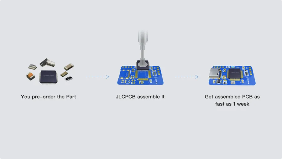
The synergy between JLCPCB, a leading PCB manufacturer, and KiCad, an open-source EDA tool, empowers electronics enthusiasts and professionals alike. This article demystifies the process of integrating these two powerful tools, providing a streamlined approach to PCB design and fabrication. From generating crucial Gerber files to leveraging plugins for efficient part sourcing and assembly, we’ll cover it all, ensuring a smooth transition from design to physical board.
Setting up Your KiCad Project for JLCPCB
Prior to generating Gerber files, meticulous configuration of your KiCad project to adhere to JLCPCB's specific design rules is paramount for a smooth and successful PCB fabrication. This initial setup involves careful consideration of track widths, clearances, and via sizes, ensuring compatibility with JLCPCB's manufacturing capabilities and preventing costly errors.
- Track Widths
Adhere to JLCPCB's minimum track width specifications, typically found in their design rule documentation. Inadequate track widths can lead to fabrication issues and poor circuit performance. - Clearances
Ensure that the spacing between copper features (tracks, pads, vias) meets JLCPCB's minimum clearance requirements. Insufficient clearances can cause shorts and fabrication failures. - Via Sizes
Select appropriate via sizes that align with JLCPCB's capabilities, paying attention to both the drill diameter and the finished via diameter. Proper via sizing is critical for reliable connectivity and manufacturing yield.
| Parameter | Typical Value for JLCPCB | Description |
|---|---|---|
| Minimum Track Width | 0.127 mm (5 mil) | Smallest width of a copper trace |
| Minimum Clearance | 0.1524 mm (6 mil) | Minimum space between copper features |
| Minimum Via Drill Diameter | 0.3 mm (12 mil) | Drill diameter for vias |
| Minimum Via Finished Diameter | 0.6 mm (24 mil) | Finished hole size after plating |
Generating Gerber Files in KiCad: A Step-by-Step Guide
Generating Gerber files correctly is paramount for successful PCB fabrication with JLCPCB. This process translates your KiCad PCB design into a format that manufacturing equipment can understand. This section provides a detailed guide to ensure that your files are accurate and compatible with JLCPCB's requirements.
The following steps detail the process of generating Gerber files in KiCad. Note that specific menu locations and dialog box layouts may differ slightly between KiCad versions, but the fundamental steps remain consistent.
- Open the PCB Editor
Launch the PCB editor within your KiCad project. Ensure your PCB layout is complete and all design rule checks (DRC) have passed. - Access the Plot Menu
Navigate to 'File' -> 'Plot' to open the plotting dialog, which will be used for Gerber file generation. - Select Gerber Format
Choose 'Gerber' as the output format from the dropdown menu. This sets the system to produce Gerber files. - Choose Layers
Select the layers you want to include in the Gerber output. For a standard two-layer board, at a minimum include: 'F.Cu' (Front Copper), 'B.Cu' (Back Copper), 'F.SilkS' (Front Silk Screen), 'B.SilkS' (Back Silk Screen), 'F.Mask' (Front Solder Mask), 'B.Mask' (Back Solder Mask). Additionally, consider including board outline layers and any additional layers like plated holes if they are present. - Set Gerber Options
Configure specific options for your Gerber files such as 'Use Protel naming' and 'exclude PCB edge layer from other layers', this ensure the Gerber files have clear filenames and accurate board boundary. - Set Output Directory
Choose a directory where the generated Gerber files will be saved. It is recommended to create a new, dedicated folder named 'gerber_files' within your project directory. - Generate Gerber Files
Click the 'Plot' button to initiate the generation of the Gerber files. This process will generate multiple files, one for each layer selected in step 4. After completion of the generation, check the files in the destination directory. - Generate Drill Files
Go to 'File' -> 'Plot' in the PCB editor. Select 'Generate Drill Files', and configure the drill file options such as using 'Drill File units (Inch)'. Then click on 'Generate Drill File'. Make sure you've saved this as a separate file to send to JLCPCB with the Gerber files.
Once the files are created, inspect the generated files using a Gerber viewer to verify the integrity of the output. This confirms that the files generated correctly represent your design and avoid any last-minute manufacturing issues.
Drill File Generation for JLCPCB Compatibility
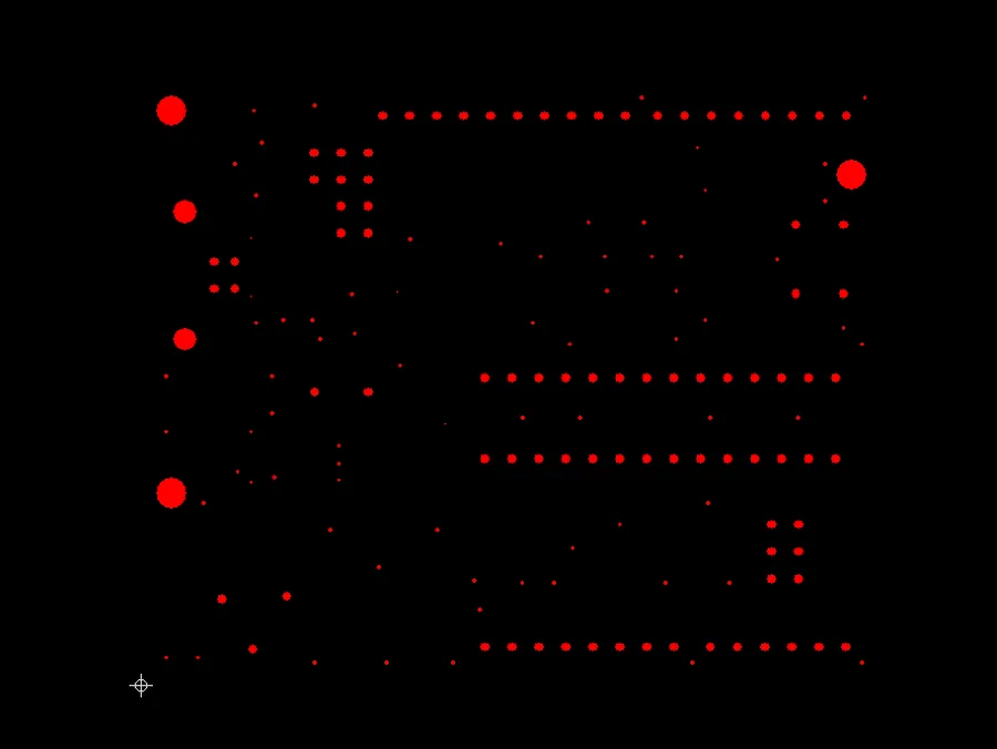
Accurate drill file generation is paramount for successful PCB fabrication at JLCPCB. These files dictate the precise locations and sizes of holes on the PCB, which are crucial for component placement and via connections. Correct settings and formats are essential to avoid manufacturing errors and ensure seamless board functionality.
Drill files, unlike Gerber files which define copper layers, solder mask, and silkscreen, provide the numerical instructions for drilling machines. They typically come in formats like Excellon or Gerber X2 with embedded drill data. Each hole is defined by its X and Y coordinates, and its diameter. Incorrectly generated drill files can lead to misplaced holes, incorrect sizes, or the omission of necessary vias, all of which will lead to a nonfunctional board.
| Parameter | Description | JLCPCB Recommendation |
|---|---|---|
| File Format | Defines the encoding method for drill data | Excellon or Gerber X2 with embedded drill data |
| Units | Specifies whether the locations and diameters of holes are in inches or millimeters | Millimeters (mm) |
| Zero Suppression | Handles leading or trailing zeros in numeric data | Trailing zeros suppressed |
| Coordinate Format | Specifies absolute or incremental coordinates of the drill | Absolute |
| Tool Definition | Specifies the size of each drill used | Clear and unique tool number for each size |
When generating drill files in KiCad for JLCPCB, ensure the settings match JLCPCB’s requirements, which usually entails setting units to millimeters and opting for an Excellon file format and set the zero suppression. Check for the appropriate coordinate format and tool size definition, these settings can usually be found in the drill file generation dialog box of KiCad.
In conclusion, generating compatible drill files requires careful attention to detail. By adhering to these guidelines, you can minimize the chances of manufacturing errors and ensure the precise execution of your PCB design at JLCPCB.
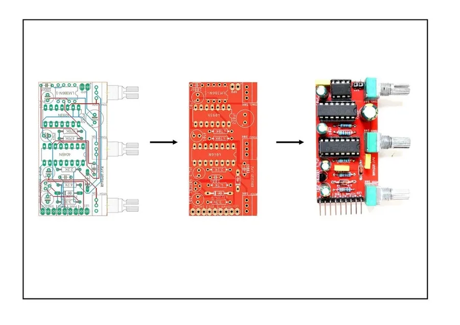
Leveraging KiCad Plugins for JLCPCB: Simplifying the Process
KiCad plugins tailored for JLCPCB significantly streamline the PCB design and manufacturing workflow. These tools facilitate parts sourcing, Bill of Materials (BOM) generation, and file preparation for assembly services, ultimately reducing errors and saving valuable time. By automating and optimizing key steps, they ensure a more efficient transition from design to production.
- Key Benefits of Using JLCPCB KiCad Plugins
These plugins offer several advantages including direct access to the JLCPCB parts library, automated BOM creation compatible with JLCPCB's assembly services, and streamlined Gerber file generation tailored to JLCPCB's requirements. - Streamlined Parts Sourcing
Plugins allow you to directly search and assign parts from the JLCPCB component library within KiCad. This ensures that your design uses components readily available and compatible for assembly. - Automated Bill of Materials (BOM) Generation
Plugins can automatically generate BOMs compatible with JLCPCB's ordering system. This ensures that all necessary component details, including part numbers, are correctly captured, preventing delays and errors. - Simplified File Preparation for Assembly Services
Plugins can prepare files necessary for PCB assembly services, including pick-and-place data, simplifying the transition from design to manufacturing. - Time and Error Reduction
By automating tedious tasks and ensuring compatibility with JLCPCB's specifications, plugins reduce the risk of errors and significantly shorten the design to fabrication cycle.
| Plugin Function | Description | Benefits |
|---|---|---|
| Parts Sourcing | Direct search and assignment of parts from the JLCPCB database within KiCad. | Ensures component availability and streamlines assembly. |
| BOM Generation | Automatic generation of Bill of Materials compatible with JLCPCB. | Reduces errors, saves time, and ensures accurate component ordering. |
| File Preparation | Prepares Gerber files, pick-and-place data, and other files needed for assembly. | Simplifies the transfer from design to manufacturing. |
JLCPCB Part Sourcing through KiCad Plugins
KiCad's integration with JLCPCB is greatly enhanced by plugins that allow for direct part sourcing from JLCPCB's component library. These plugins bridge the gap between design and manufacturing, enabling engineers to select components that are readily available and compatible with JLCPCB's assembly capabilities, significantly streamlining the PCB assembly process.
These plugins facilitate a direct connection to the JLCPCB parts database within the KiCad environment. This enables users to search for specific components, view their availability, pricing, and specifications directly from within KiCad's schematic or PCB layout editors. This direct access ensures that only parts that can be reliably sourced and assembled are selected for the project.
- Direct Component Search
Plugins enable users to search the JLCPCB parts database using keywords, part numbers, or specifications directly from within KiCad. - Availability and Pricing
Real-time information on component availability, pricing, and lead times is displayed, allowing engineers to make informed decisions. - Component Assignment
Selected components can be directly assigned to footprints within KiCad, automating the part selection process. - Bill of Materials (BOM) Generation
The plugin can generate a precise Bill of Materials based on the selected components, which simplifies the ordering process with JLCPCB. - Assembly Compatibility Checks
Plugins often include features to check if selected components are compatible with JLCPCB's assembly processes, preventing errors and ensuring manufacturability.
Optimizing KiCad Design Rules for JLCPCB
Adhering to specific design rules in KiCad is paramount for ensuring your PCB design is compatible with JLCPCB's manufacturing processes, preventing costly fabrication issues. This involves configuring settings related to solder mask, paste, clearances, and track widths to match JLCPCB's capabilities, and understanding these requirements is crucial for successful PCB production.
| Design Rule | JLCPCB Requirement | KiCad Setting | Rationale |
|---|---|---|---|
| Minimum Track Width | 6 mil (0.1524 mm) | Design Rules -> Net Classes -> Track Width | Ensures tracks are thick enough to be properly etched during fabrication. |
| Minimum Track Clearance | 6 mil (0.1524 mm) | Design Rules -> Net Classes -> Clearance | Prevents shorts by ensuring adequate spacing between conductive elements. |
| Minimum Via Diameter | 0.3 mm | Design Rules -> Via Sizes | Ensures vias are large enough to be reliably drilled and plated. |
| Minimum Annular Ring | 5 mil (0.127 mm) | Design Rules -> Via Sizes -> Annular Ring | Provides sufficient copper around via holes for reliable electrical connection. |
| Solder Mask Clearance | 4 mil (0.1016 mm) | Design Rules -> Solder Mask -> Clearance | Prevents solder mask from covering pads, ensuring proper soldering. |
| Solder Paste Clearance | 4 mil (0.1016 mm) | Design Rules -> Solder Paste -> Clearance | Ensures solder paste is applied correctly during reflow, allowing for proper solder joints. |
| Minimum Drill Size | 0.3 mm | Design Rules -> Drill Sizes | Ensures reliable drilling and consistent via and hole size. |
Properly setting these design rules within KiCad ensures that your PCB design aligns with JLCPCB's manufacturing standards, minimizing the risk of errors and delays during production. It's crucial to always refer to the latest JLCPCB manufacturing specifications, which are available on their website, as these specifications may be updated.
Frequently Asked Questions About JLCPCB and KiCad Integration
This section addresses common questions encountered when integrating KiCad with JLCPCB for PCB fabrication, providing clear solutions to typical challenges and aiming for a smooth and efficient production workflow.
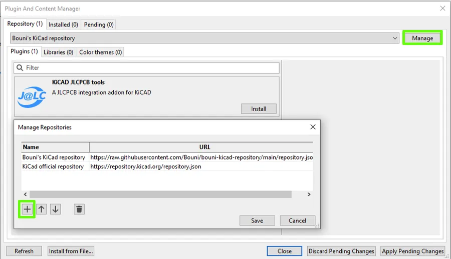
- Which KiCad plugin is best for JLCPCB?
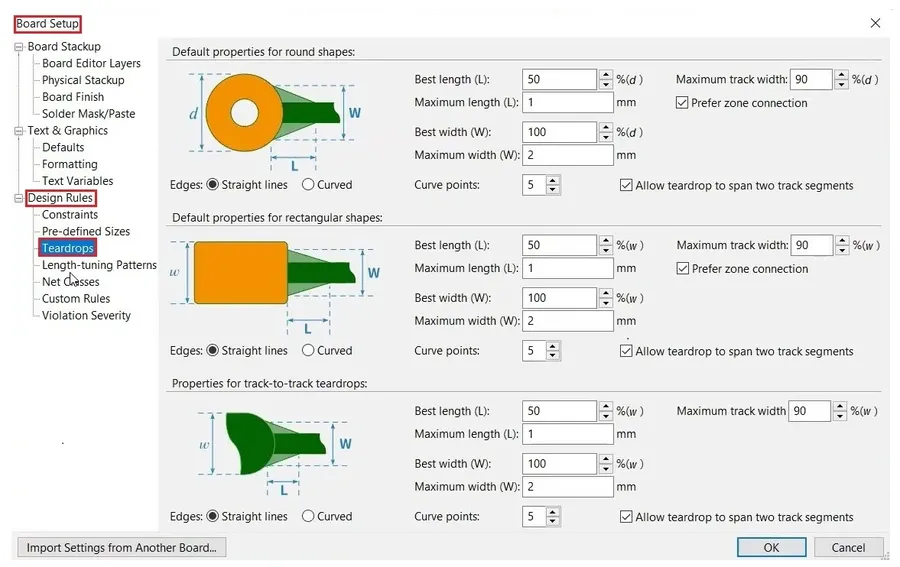
The 'JLCPCB Tools' plugin is highly recommended for its direct integration with JLCPCB's parts library, ordering system, and file preparation capabilities. It simplifies the process of generating Gerber files, BOMs, and pick-and-place files, minimizing the chance of errors. It is also actively maintained and updated to ensure compatibility with the latest KiCad version and JLCPCB's requirements. - How do I resolve minimum solder width errors for JLCPCB in KiCad?
Minimum solder mask widths are a common design rule constraint that must be adhered to for reliable PCB fabrication. In KiCad, adjust the design rules in 'File' -> 'Board Setup' -> 'Design Rules' tab, specifically setting the 'Solder Mask' settings to meet JLCPCB's specifications. It's important to note that different mask sizes can impact manufacturability, so ensure there is a proper overlap, typically of 0.1mm or 4mil on all pads to make sure your mask doesn't overlap pads that are not connected. - What file formats does JLCPCB require for PCB manufacturing?
JLCPCB primarily requires Gerber files (RS-274X format) for PCB layers, along with a drill file (Excellon format). Ensure that you generate these file types correctly from KiCad, including all necessary layers (copper, silkscreen, solder mask, etc.). Additionally, for assembly services, you'll need a BOM and a pick-and-place file, which can be produced through the 'JLCPCB Tools' or 'BOM Export' plugin. - What should I do if my Gerber files fail JLCPCB's checks?
If JLCPCB's online Gerber viewer shows issues, carefully review the error messages, such as missing layers, or incorrect dimensions. Double-check your Gerber settings in KiCad, ensuring all required layers are included and properly configured for their respective functions. Also, check design rule violations like track width, clearance, and via size which can cause issues in the Gerber generation. For best results, use the JLCPCB plugin for file generation to prevent common errors. - Can I directly order components from JLCPCB using KiCad?
Yes, using the 'JLCPCB Tools' plugin, you can directly search and assign components from JLCPCB's parts library. This allows you to verify if parts are in stock and ensures compatibility with their assembly services. By linking components directly from JLCPCB, you also reduce the risk of purchasing incompatible parts or having to make changes later in your design cycle. - How to ensure that my KiCad project is optimized for JLCPCB assembly?
To ensure your project is optimized, you must use the correct design rules for spacing, minimum trace width, and pad sizes as per JLCPCB's capabilities. It is crucial that the BOM and pick-and-place file are complete and accurately reflect the design. Double-check all values against the JLCPCB parts library. When possible, use standard footprints as defined by the manufacturer to ensure smooth assembly and reduce risk of fabrication issues - How do I handle different KiCad versions with JLCPCB?
While most standard functionalities remain consistent across KiCad versions, plugins may be version-specific. Always use the latest version of the 'JLCPCB Tools' plugin compatible with your version of KiCad. JLCPCB's documentation and online resources are regularly updated to reflect changes in KiCad and provide necessary guidance for different KiCad version users.
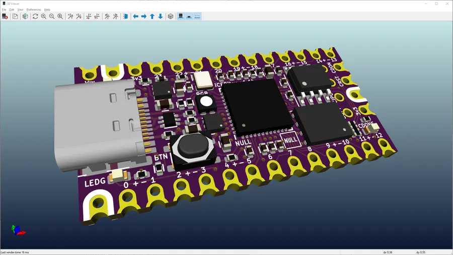
Advanced Features: 3D Models and STEP File Integration with JLCPCB and KiCad
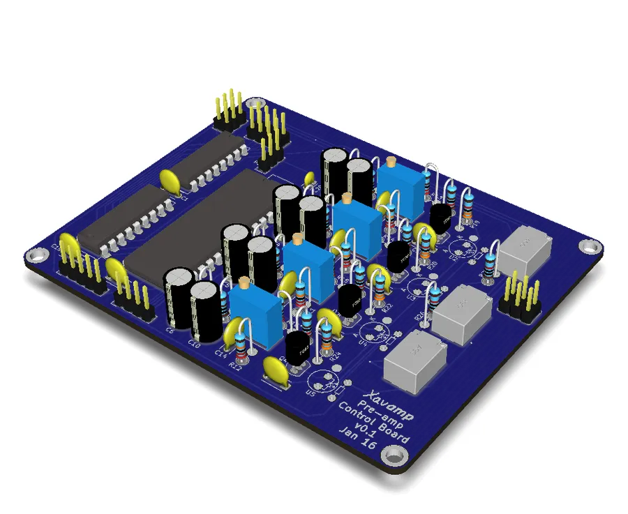
Integrating 3D models into your KiCad PCB designs, particularly using STEP files from JLCPCB, significantly enhances the design process by providing realistic visualizations and ensuring mechanical accuracy. This capability allows for a more comprehensive understanding of how the final product will look and fit together, before actual fabrication.
This section explores how to effectively utilize STEP files, including how to download them from JLCPCB's part library, incorporate them into your KiCad project, and ensure proper alignment with your PCB layout. We will also discuss why this step is crucial for complex designs or when mechanical integration is a key consideration.
- Benefits of 3D Model Integration
Utilizing 3D models, particularly STEP files, enhances your KiCad projects in several ways. The ability to visualize the PCB assembly before physical production allows for the early detection of mechanical conflicts or fit issues, saving time and costs on potential design revisions. - JLCPCB's STEP File Library
JLCPCB offers a vast library of STEP files for many of their parts. These files can be directly downloaded and used in KiCad, providing accurate 3D representations for realistic PCB modeling. This eliminates the need to model components from scratch, ensuring high accuracy and efficient design workflows. - Downloading and Converting STEP files for KiCad
STEP files can be downloaded directly from JLCPCB's component database. Once downloaded, these files can be easily imported into KiCad, typically into the 3D model properties of a component. KiCad uses a variety of standard 3D file formats, and STEP files are one of the most popular for component models due to their accuracy.
| Feature | Description | Benefit |
|---|---|---|
| Realistic Visualization | 3D models allow a view of the assembled PCB. | Early detection of mechanical issues. |
| Mechanical accuracy | STEP files provide precise dimensions. | Ensures correct fit within enclosures. |
| Design workflow | Direct import into KiCad from the JLCPCB part database. | Saves time and effort over creating models from scratch. |
Troubleshooting Common Issues with JLCPCB and KiCad
Encountering issues when integrating KiCad designs with JLCPCB for fabrication is common, primarily stemming from file format mismatches, incorrect output settings, or design rule violations. This section addresses typical problems and offers practical solutions to ensure a smooth and successful PCB production process.
- Gerber File Generation Errors
Incorrect layer selection or output format during Gerber generation can lead to missing or incomplete data. Ensure the correct layers are chosen (copper, silkscreen, solder mask, etc.) and that the output format aligns with JLCPCB's specifications (typically RS-274X). - Drill File Issues
Incompatibility of drill files, often due to incorrect format (e.g., Excellon) or missing units (e.g., mm or inches), can cause fabrication problems. Verify the drill file format matches JLCPCB's requirements and that units are correctly specified in the settings. - File Naming Conventions
Using incorrect or non-standard file names can lead to misinterpretation or rejection by JLCPCB's system. Stick to accepted file naming standards (e.g., layer names and extensions) to ensure clarity and smooth processing. - Design Rule Check (DRC) Failures
DRC violations, such as insufficient track width, clearance, or via sizes, can lead to fabrication errors. Always run the DRC in KiCad using JLCPCB's design rules to prevent issues before uploading files. Update KiCad DRC settings with JLCPCB manufacturing specifications. - Component Placement and Rotation Issues
Component placement or rotation issues identified by JLCPCB's assembly service can result from errors in the component library or pick-and-place file generation. Double-check part rotation within KiCad and ensure the correct orientation is specified in your BOM and pick-and-place file. - BOM and Pick and Place Discrepancies
Inconsistencies between the BOM and pick-and-place file can cause delays or assembly errors. Verify the generated BOM matches component placement in the design, ensuring all parts are correctly referenced in both file types.
Integrating JLCPCB with KiCad provides a powerful workflow for PCB design and fabrication. By understanding the nuances of Gerber generation, plugin usage, and design rule optimization, you can streamline your workflow, avoid common pitfalls, and achieve high-quality, manufacturable PCBs. Utilizing KiCad's capabilities to work effectively with JLCPCB ensures a seamless process from schematic design to a finished product, fostering innovation and efficiency in electronics development.