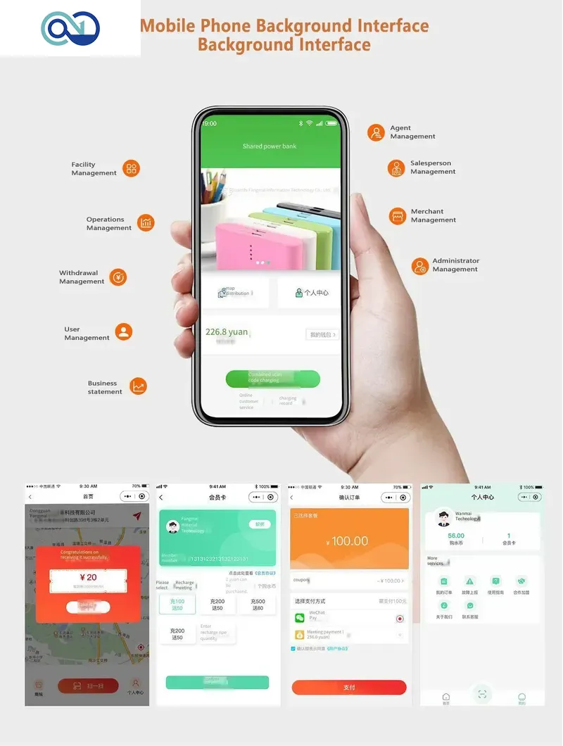
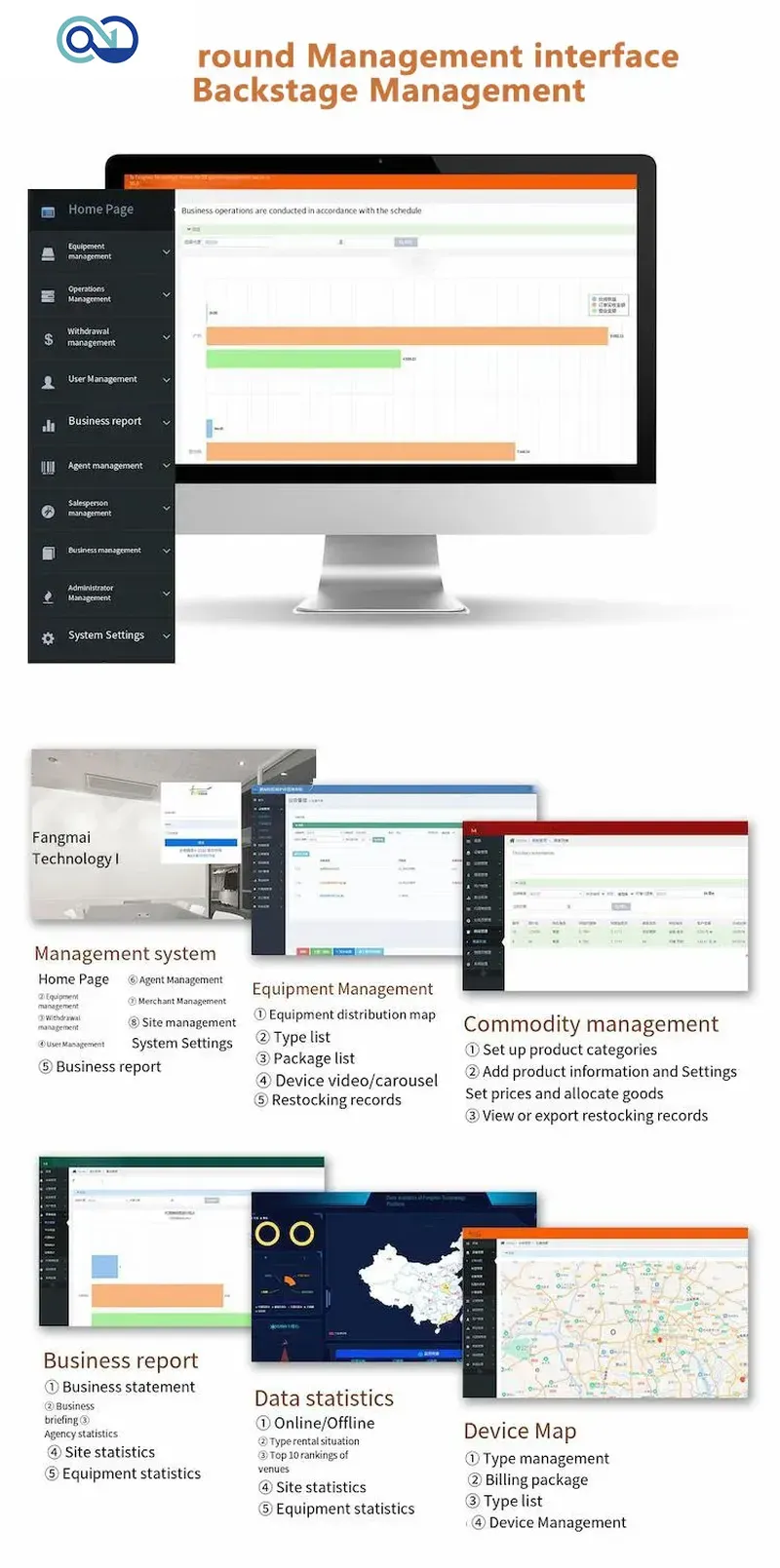
Shared Umbrella Solution

In the fast-paced world of electronics manufacturing, getting your product to market quickly and efficiently is paramount. Imagine having a reliable partner that provides comprehensive PCB solutions, from initial design to final assembly, all under one roof. This 'Shared Umbrella Solution' is precisely what Zero One Solution Limited offers, acting as your one-stop shop for all PCB needs. Let's explore how this approach streamlines the prototyping and production process, accelerating innovation and reducing time-to-market.
Introduction to Shared Umbrella PCB Solutions

A 'Shared Umbrella' PCB solution represents a comprehensive and integrated approach to printed circuit board (PCB) services, where a single provider manages all aspects from initial design and prototyping to manufacturing, assembly, and testing. This holistic strategy offers numerous benefits, streamlining the entire PCB development process and fostering efficiency, consistency, and reliability.
At its core, the 'Shared Umbrella' concept aims to consolidate all PCB-related needs under one roof, eliminating the complexities and potential communication breakdowns that can arise from working with multiple vendors. This integrated model ensures seamless coordination, faster turnaround times, and a more cohesive approach to problem-solving.
- What are the primary advantages of choosing a Shared Umbrella PCB solution?
The key benefits include reduced lead times due to streamlined processes, enhanced communication and collaboration, cost savings through economies of scale, improved quality control, and simplified project management. - How does a Shared Umbrella approach improve PCB quality?
By having a single provider oversee all stages of PCB development, quality control is integrated into every step. This allows for early detection and correction of potential issues, leading to higher overall quality and reliability. - What types of businesses benefit most from this type of solution?
Businesses of all sizes can benefit, but it is particularly advantageous for companies that require rapid prototyping, complex PCB designs, or high-volume production runs. It’s also ideal for companies looking to simplify their supply chain and reduce administrative overhead. - Can a Shared Umbrella PCB provider handle both small and large production runs?
Yes, a capable Shared Umbrella provider should be equipped to handle a wide range of production volumes, from small prototype batches to large-scale manufacturing runs, offering flexibility and scalability to meet evolving needs. - How does a Shared Umbrella solution facilitate faster turnaround times?
Consolidating all processes under one provider eliminates delays associated with vendor handoffs and communication gaps. This streamlined approach allows for quicker design iterations, faster manufacturing, and reduced overall project timelines. - What is the role of rapid prototyping in a Shared Umbrella PCB service?
Rapid prototyping is a crucial component, enabling quick testing and validation of designs. A Shared Umbrella provider with strong prototyping capabilities can significantly accelerate product development cycles. - How does Zero One Solution Limited exemplify a Shared Umbrella PCB provider?
Zero One Solution Limited provides a comprehensive suite of PCB services, from design and manufacturing to assembly, testing, and supply chain management. Our expertise, strategic locations, and commitment to rapid prototyping make us an ideal partner for companies seeking a streamlined and efficient PCB solution.
Zero One Solution Limited: Your Strategic Partner

Zero One Solution Limited stands as a strategic partner in the PCB industry, leveraging years of expertise and a commitment to rapid prototyping and comprehensive, one-stop services. Since our inception in 2011, we have been dedicated to empowering clients with accelerated product development cycles and innovative solutions, making us a trusted name in PCBA solutions.
Our deep understanding of the PCB landscape, combined with a customer-centric approach, allows us to provide tailored solutions that meet the unique needs of each client. From initial design to final assembly, we ensure a seamless and efficient process, reducing time-to-market and maximizing ROI.
- What specific PCB services does Zero One Solution Limited offer?
Zero One Solution Limited provides a complete suite of PCB services, including PCB design, manufacturing, assembly, and testing. Our one-stop service approach ensures seamless integration and efficient project management from start to finish. - How does Zero One Solution Limited ensure the quality of its PCB solutions?
Quality is paramount at Zero One Solution Limited. We adhere to stringent quality control measures at every stage of the PCB process, from design to assembly, and comply with industry standards such as IPC-A-610. Our commitment to quality ensures reliable and high-performance PCB solutions. - What are the benefits of choosing Zero One Solution Limited as a PCB partner?
Partnering with Zero One Solution Limited offers numerous advantages, including rapid prototyping, reduced lead times, cost savings, and improved communication. Our expertise, comprehensive services, and global reach enable us to deliver exceptional value and support to our clients. - How does Zero One Solution Limited support rapid prototyping?
We excel in rapid prototyping, providing quick-turnaround services that enable clients to test and refine their designs efficiently. Our advanced manufacturing capabilities and streamlined processes allow us to deliver prototypes in a fraction of the time compared to traditional methods, accelerating product development. - Where are Zero One Solution Limited's primary locations?
Our headquarters is strategically located in Shenzhen, China, the heart of electronic manufacturing. We also have a branch office in Dubai, allowing us to serve clients worldwide and ensure seamless access to global resources and support. - What industries does Zero One Solution Limited serve?
Zero One Solution Limited serves a diverse range of industries, including consumer electronics, telecommunications, automotive, medical devices, and industrial automation. Our versatile PCB solutions cater to the unique requirements of each industry, delivering reliable and high-performance results.
The Breadth of Services: From Design to Assembly

Zero One Solution Limited offers a complete suite of PCB services, covering every stage from initial design to final assembly, ensuring a streamlined and efficient process for our clients. Our comprehensive approach minimizes communication overhead, reduces lead times, and ensures seamless integration between each phase of the PCB development lifecycle.
- PCB Design and Layout
Our expert team utilizes industry-leading software to create optimized PCB layouts that meet your specific requirements, including signal integrity analysis, thermal management, and manufacturability considerations. - Component Selection and Sourcing
We assist in selecting the most suitable components for your application, leveraging our extensive network of trusted suppliers to ensure quality and availability. - PCB Manufacturing
We provide high-quality PCB manufacturing services, supporting a wide range of materials, layer counts, and fabrication technologies to meet diverse project needs. Our capabilities include quick-turn prototyping and volume production. - PCB Assembly
Our advanced assembly lines are equipped to handle SMT, through-hole, and mixed technology assembly, ensuring precise component placement and reliable soldering. We offer automated optical inspection (AOI) and X-ray inspection to guarantee quality. - Testing and Quality Assurance
We conduct rigorous testing, including functional testing, in-circuit testing (ICT), and environmental testing, to verify PCB performance and reliability. Our quality assurance processes adhere to industry standards such as IPC-A-610. - Supply Chain Management
Zero One Solution offers complete supply chain management solutions, from component procurement and inventory management to logistics and delivery, streamlining the entire process for our clients. - DFM/DFA Checks
Design for Manufacturing (DFM) and Design for Assembly (DFA) checks are integral to our process, identifying potential issues early in the design phase to prevent costly rework and ensure efficient production.
Rapid Prototyping: Accelerating Innovation
Rapid prototyping is indispensable for accelerating innovation in product development. It allows for quick iteration, validation of design concepts, and early detection of potential issues. Zero One Solution facilitates this crucial process by providing efficient and high-quality rapid prototyping services, enabling clients to bring innovative solutions to market faster and with greater confidence.
At Zero One Solution Limited, we understand that time is of the essence in today's competitive market. Our rapid prototyping services are designed to help you quickly test and refine your PCB designs, minimizing time-to-market and maximizing your return on investment. We leverage advanced technologies and streamlined processes to deliver prototypes with exceptional speed and precision.
- What is the typical turnaround time for PCB rapid prototyping at Zero One Solution?
Our typical turnaround time for PCB rapid prototyping ranges from 24 hours to 5 days, depending on the complexity and quantity of the design. We prioritize speed without compromising quality. - What types of PCB prototypes can Zero One Solution manufacture?
We can manufacture a wide range of PCB prototypes, including single-layer, multi-layer, rigid, flexible, and rigid-flex PCBs. We support various materials, finishes, and technologies to meet your specific requirements. - How does rapid prototyping reduce development costs?
Rapid prototyping allows you to identify design flaws and optimize performance early in the development cycle, avoiding costly rework and redesign later on. This streamlined approach significantly reduces overall development costs. - What data do I need to provide for rapid prototyping?
To start the rapid prototyping process, you'll need to provide your PCB design files (Gerber files), bill of materials (BOM), and any specific manufacturing instructions or requirements. Our team is available to assist you with file preparation and optimization. - Can Zero One Solution assist with design modifications during the prototyping phase?
Yes, we offer comprehensive design support and can assist with design modifications based on the results of your prototype testing. Our experienced engineers provide valuable feedback and guidance to optimize your PCB design for performance and manufacturability. - What quality control measures are in place for rapid prototyping?
We maintain stringent quality control measures throughout the rapid prototyping process, including automated optical inspection (AOI), electrical testing, and dimensional verification. Our commitment to quality ensures that your prototypes meet the highest standards. - Does Zero One Solution offer assembly services for PCB prototypes?
Yes, we provide full assembly services for PCB prototypes, including component sourcing, placement, soldering, and testing. Our one-stop solution simplifies the prototyping process and ensures seamless integration between manufacturing and assembly.
Global Reach, Local Expertise: Shenzhen and Dubai
Zero One Solution Limited strategically positions itself in Shenzhen, China, and Dubai to optimize supply chain efficiency and provide comprehensive global support. These locations are not merely offices; they are pivotal hubs within the global PCBA ecosystem, designed to enhance responsiveness and accessibility for our clients worldwide.
Here’s how our strategic locations benefit you:
- Shenzhen: The Heart of Electronics Manufacturing
Located in the epicenter of China's electronics manufacturing hub, our Shenzhen headquarters provides unparalleled access to a vast network of suppliers, cutting-edge technologies, and skilled labor. This proximity allows us to offer rapid prototyping and efficient mass production, ensuring high-quality PCBs at competitive prices. - Dubai: Bridging East and West
Our Dubai branch acts as a strategic bridge between Eastern and Western markets. This location facilitates seamless communication, streamlined logistics, and localized support for clients in the Middle East, Europe, and Africa. Dubai's central time zone and business-friendly environment make it an ideal hub for managing international projects and ensuring timely delivery. - Enhanced Supply Chain Efficiency
By operating in both Shenzhen and Dubai, we optimize our supply chain to reduce lead times and minimize disruptions. This dual presence enables us to source components globally, manage inventory effectively, and adapt quickly to changing market conditions, ensuring a reliable and cost-effective PCB supply for our clients. - Localized Support and Expertise
Our strategic locations allow us to provide localized support tailored to the specific needs of our clients in different regions. Whether it's navigating local regulations, understanding cultural nuances, or providing on-site technical assistance, our teams in Shenzhen and Dubai are equipped to deliver exceptional service and build long-term partnerships. - Global PCBA Supply Chain Network
Zero One Solution Limited's presence in Shenzhen and Dubai ensures seamless access to a global PCBA supply chain network. This network enables us to leverage worldwide resources and support, providing our clients with a competitive edge in the market. We are committed to delivering innovative solutions and exceptional service, no matter where our clients are located.
Benefits of a Shared Umbrella Approach
Adopting a 'Shared Umbrella Approach' with Zero One Solution Limited offers a multitude of benefits by centralizing all your PCB needs under a single, expert provider. This strategy streamlines operations, reduces complexities, and enhances overall project efficiency, ensuring a smoother path from design to final product.
Here are some key advantages of choosing Zero One Solution as your comprehensive PCB partner:
- Reduced Lead Times
By integrating design, manufacturing, and assembly processes, we significantly shorten lead times. This is because communication delays are minimized, and workflows are optimized, allowing for faster turnaround on prototypes and production runs. Zero One Solution's rapid prototyping capabilities further accelerate this process. - Improved Communication and Collaboration
With a single point of contact for all PCB-related matters, communication becomes seamless and efficient. This eliminates the risk of misunderstandings and ensures that all teams are aligned on project goals and specifications. Enhanced collaboration leads to better problem-solving and faster issue resolution. - Cost Savings
A consolidated approach can lead to significant cost savings through economies of scale, optimized resource allocation, and reduced administrative overhead. Zero One Solution's strategic locations in Shenzhen and Dubai further contribute to cost-effectiveness by leveraging global supply chain efficiencies. - Enhanced Quality Control
Having all processes under one roof allows for stringent quality control measures at every stage, from design to assembly. This reduces the risk of defects and ensures that the final product meets the highest standards of performance and reliability. Our commitment to quality is unwavering. - Simplified Supply Chain Management
Managing multiple vendors can be complex and time-consuming. By partnering with Zero One Solution, you simplify your supply chain, reduce logistical challenges, and gain better visibility into the entire PCB production process. This streamlined approach minimizes risks and improves overall efficiency. - Access to a Wide Range of Expertise
Zero One Solution brings together a team of experts in PCB design, manufacturing, and assembly. This diverse skill set ensures that you have access to the best knowledge and resources for every aspect of your project. Our team's experience and expertise are invaluable assets for our clients.
Case Studies: Real-World Applications
The true measure of a PCB solution provider lies in its ability to deliver tangible results. At Zero One Solution Limited, we pride ourselves on transforming innovative ideas into market-ready products through our comprehensive suite of PCB services. The following case studies illustrate how our 'Shared Umbrella Solution' has enabled clients to overcome challenges, accelerate development cycles, and achieve remarkable success.
While specific client details are kept confidential, the following scenarios highlight the types of challenges we address and the positive outcomes we deliver:
- Aerospace Innovation: Streamlining Complex PCB Design for Satellite Communication
Challenge: An aerospace company faced significant delays in developing a new satellite communication system due to the complexity of the PCB design and the need for miniaturization. Solution: Zero One Solution provided an end-to-end service, from initial design consultation to final assembly, optimizing the PCB layout for signal integrity and thermal management. Outcome: The client reduced their development time by 40% and successfully launched their product within budget. - Medical Device Advancement: Rapid Prototyping for a Cutting-Edge Diagnostic Tool
Challenge: A medical device startup needed a rapid prototype of a highly sensitive diagnostic tool with stringent performance requirements. Solution: Leveraging our rapid prototyping capabilities, Zero One Solution delivered a functional prototype within two weeks, allowing the client to secure further funding and accelerate clinical trials. Outcome: The startup successfully demonstrated the feasibility of their technology, attracting significant investment and paving the way for regulatory approval. - Industrial Automation: Enhancing Reliability of Control Systems in Harsh Environments
Challenge: An industrial automation firm struggled with the reliability of their control systems operating in harsh environments with extreme temperatures and vibrations. Solution: Zero One Solution provided robust PCB manufacturing and assembly services, using high-quality components and conformal coating to ensure long-term durability. Outcome: The client significantly reduced system downtime and maintenance costs, improving overall operational efficiency. - Consumer Electronics: Optimizing PCB Design for High-Volume Production of Smart Devices
Challenge: A consumer electronics company aimed to optimize the PCB design for their new smart device to minimize manufacturing costs and improve yield. Solution: Zero One Solution provided design for manufacturability (DFM) analysis and optimization, identifying potential issues and recommending design modifications. Outcome: The client achieved a 20% reduction in manufacturing costs and a 15% improvement in yield, resulting in significant savings and increased profitability. - Telecommunications Infrastructure: Developing High-Performance PCBs for 5G Networks
Challenge: A telecommunications company required high-performance PCBs for their 5G network infrastructure, capable of handling high frequencies and data rates. Solution: Zero One Solution provided advanced PCB fabrication services, using specialized materials and processes to meet the demanding performance requirements. Outcome: The client successfully deployed their 5G network with enhanced speed and reliability, gaining a competitive edge in the market.
These case studies demonstrate the versatility and effectiveness of Zero One Solution's 'Shared Umbrella Solution' across various industries. By partnering with us, clients gain access to a comprehensive suite of services, technical expertise, and a commitment to delivering exceptional results.
Future Trends in PCB Solutions
The PCB industry is on the cusp of transformative change, driven by advancements in technology, materials, and manufacturing processes. Zero One Solution Limited is proactively adapting to these emerging trends to provide cutting-edge solutions for our clients. We are committed to staying ahead of the curve, ensuring that our services align with the evolving needs of the electronics industry. By embracing these future trends, Zero One Solution empowers clients to design more sophisticated, efficient, and reliable electronic products.
- High-Density Interconnect (HDI) PCBs
HDI PCBs are increasingly in demand due to the growing need for miniaturization and higher performance in electronic devices. These boards feature finer lines and spaces, microvias, and advanced materials to pack more functionality into smaller areas. Zero One Solution is investing in advanced equipment and expertise to manufacture complex HDI PCBs with precision and reliability. - Flexible and Rigid-Flex PCBs
Flexible PCBs and rigid-flex PCBs are gaining popularity for their ability to conform to unique shapes and spaces, offering greater design freedom and reliability in applications such as wearables, medical devices, and automotive electronics. Zero One Solution offers comprehensive services for designing and manufacturing flexible and rigid-flex PCBs, enabling clients to create innovative products with enhanced functionality. - Advanced Materials
The demand for advanced PCB materials, such as PTFE, ceramics, and high-Tg FR-4, is rising due to their superior electrical, thermal, and mechanical properties. These materials enable PCBs to operate at higher frequencies, temperatures, and power levels, making them suitable for demanding applications. Zero One Solution is partnering with leading material suppliers to offer a wide selection of advanced materials for PCB manufacturing. - 3D Printing of PCBs
3D printing of PCBs is an emerging technology that offers rapid prototyping and customized manufacturing of electronic circuits. This technology enables designers to create complex geometries and embedded components, opening up new possibilities for electronic product design. Zero One Solution is exploring the potential of 3D printing for PCBs to offer innovative solutions for rapid prototyping and low-volume production. - Embedded Components
Embedding components within the PCB layers is a technique that improves circuit density, reduces signal noise, and enhances thermal management. This approach is particularly useful for high-frequency and high-power applications where performance and reliability are critical. Zero One Solution offers services for embedding components within PCBs, enabling clients to create high-performance electronic products. - Sustainability and Eco-Friendly Practices
There is a growing emphasis on sustainable manufacturing practices in the PCB industry, including the use of eco-friendly materials, energy-efficient processes, and waste reduction strategies. Zero One Solution is committed to minimizing its environmental impact by implementing sustainable practices throughout its operations.
FAQs About PCB Solutions
Navigating the world of PCB solutions can be complex. This section addresses frequently asked questions to provide clarity on PCB design, manufacturing, and assembly processes, helping you make informed decisions for your projects.
- What is PCB assembly, and why is it important?
PCB assembly involves mounting electronic components onto a printed circuit board. It's crucial because it transforms a bare board into a functional electronic module or device. Proper assembly ensures reliable electrical connections and performance, directly impacting the product's overall quality and lifespan. - What design considerations are most critical for PCB manufacturing?
Key design considerations include trace width and spacing for signal integrity and manufacturability, via placement for efficient layer transitions, component placement to optimize signal paths and thermal management, and adherence to design for manufacturability (DFM) guidelines to prevent manufacturing defects. - How does rapid prototyping benefit my PCB project?
Rapid prototyping allows for quick testing and validation of your PCB design, enabling you to identify and correct errors early in the development process. This significantly reduces time-to-market, minimizes costly revisions, and helps ensure the final product meets your specifications and performance requirements. - What are the common causes of PCB failure, and how can they be prevented?
Common causes include poor soldering, component defects, environmental factors like moisture and temperature, and design flaws. Prevention involves rigorous quality control during manufacturing, selecting high-quality components, implementing proper environmental protection measures, and adhering to robust design practices. - How do Shenzhen and Dubai locations enhance Zero One Solution's PCB services?
Our Shenzhen location provides access to a mature electronics manufacturing ecosystem, enabling efficient sourcing of components and cost-effective production. The Dubai office facilitates closer engagement with clients in the Middle East and Europe, offering localized support and streamlined logistics for global projects. - What file formats are required for PCB manufacturing?
Gerber files are the standard for PCB manufacturing, detailing each layer of the board, drill locations, and other critical information. Other useful files include a bill of materials (BOM) listing all components, a centroid file (pick-and-place file) for automated assembly, and any specific instructions or drawings. - How can I get a quote for my PCB project?
To receive a quote, provide us with your Gerber files, BOM, quantity requirements, and any specific manufacturing instructions. Our team will review your requirements and provide a detailed, competitive quote tailored to your project's needs.
In conclusion, Zero One Solution Limited's Shared Umbrella Solution offers a comprehensive and efficient approach to PCB design, manufacturing, and assembly. By providing a one-stop service, we empower our clients to accelerate their product development cycles, reduce costs, and ultimately bring innovative solutions to market faster. Contact us today to learn how our expertise can benefit your next project. Visit our website or call our Shenzhen or Dubai office to get started. Let Zero One Solution be your trusted partner in PCB excellence.
 AnyPCBA