Single Layer PCB: A Comprehensive Guide to Design, Applications, and Manufacturing
In our daily lives, we're surrounded by technology, with circuit boards at the core of many electronic devices. Among them, the single layer PCB, a foundational component, stands out for its simplicity and cost-effectiveness. This article dives into the depths of single layer PCBs, explaining their design, applications, and how they compare to their more complex counterparts, aiming to provide you with a clear and comprehensive understanding.
Understanding Single Layer PCBs
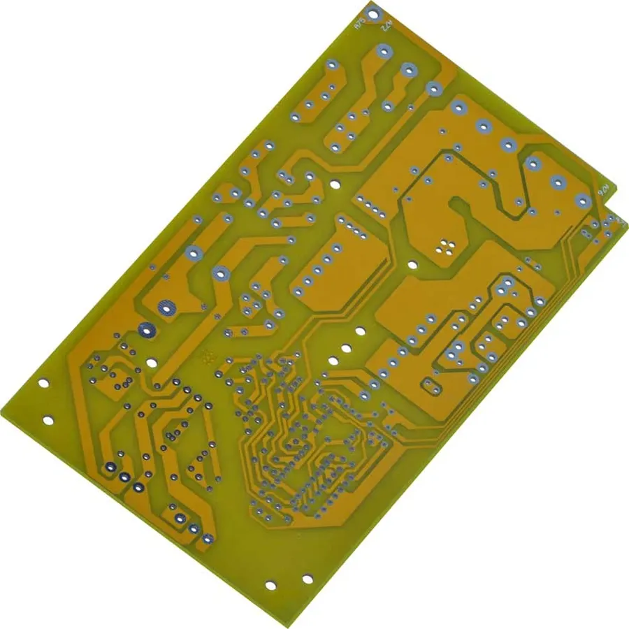
A single-layer Printed Circuit Board (PCB) is a fundamental type of circuit board characterized by having all conductive traces and components on one side of a dielectric substrate. This construction simplifies manufacturing and reduces cost, making it suitable for various low-complexity electronic applications. The core structure comprises a base material, typically a rigid or flexible dielectric, upon which a conductive layer, most often copper, is adhered. This single conductive layer defines the circuit pathways and allows components to be interconnected.
The selection of base material is crucial, influencing the PCB's electrical and mechanical properties. Materials like FR-4, a fiberglass-reinforced epoxy laminate, are commonly used for their balance of cost, durability, and electrical insulation. The copper layer, which can range from 17.5 μm to 105 μm in thickness, is essential for conducting electrical signals across the board. The copper is patterned through an etching process to form the desired circuitry. Understanding these foundational aspects is essential for effective design and application of single-layer PCBs.
Single Layer PCB Design Principles
Effective single-layer PCB design hinges on meticulous planning and adherence to best practices. This section outlines key considerations for trace routing, component placement, and via utilization to ensure optimal functionality and manufacturability. A well-executed design minimizes potential signal integrity issues and manufacturing challenges.
- Trace Width and Spacing
Carefully calculate trace width to handle the required current without overheating, and maintain adequate spacing between traces to prevent shorts and signal interference. The current carrying capacity of a trace is proportional to its cross-sectional area, so wider traces can handle more current. IPC-2221 provides guidance on minimum trace widths for specific current ratings. Ensure the trace width is consistent for the same signals to have consistent impedance. - Component Placement
Strategic component placement is crucial. Place components to minimize trace lengths and crossings, which reduces signal path impedance and complexity. Place heat-generating components to ensure adequate ventilation and heat dissipation. If possible, separate analog and digital components to reduce noise coupling. Orient the component for easy soldering and manufacturing. - Via Usage
Although single-layer PCBs have limited use for vias, you can use them to connect different parts of the circuit and change the direction of the traces. Proper via design and placement is crucial to achieve signal continuity. While vias for multi-layer PCB are used for vertical interconnections between different layers, vias in single-layer PCBs can be used as test points, or if necessary to route traces around obstacles. Minimize the number of vias as every via creates impedance mismatch. - Optimal Layout for Functionality
Consider the overall signal flow and functionality when laying out the circuit. Plan for short, direct signal paths and strategically place connectors. If necessary, plan for ground planes in critical sections to reduce signal noise. Make sure that layout is manufacturable. For example, avoid placing pads too close to the PCB edge and make sure there is adequate spacing around the components.
Single Layer PCB Manufacturing Process

The fabrication of a single-layer PCB involves a series of precise steps, transforming raw materials into a functional circuit board. This process includes substrate preparation, copper deposition, circuit patterning, protective coating, and rigorous quality checks, ensuring each board meets the required specifications.
- Substrate Preparation
The process begins with the selection of a suitable substrate material, typically a rigid laminate like FR-4. This material is then cut to the desired size and cleaned to remove any surface contaminants, preparing it for subsequent processing. The substrate provides the foundational mechanical structure for the PCB. - Copper Layering
A thin layer of copper is then applied to the substrate. This is commonly done using a chemical deposition process, creating a uniform conductive layer over the entire board surface. This copper layer will serve as the conductive traces of the PCB, carrying electrical signals between components. - Circuit Patterning (Etching)
To define the precise conductive pathways, a photoresist material is applied to the copper layer, followed by exposure to a UV light source through a photomask that represents the desired circuit pattern. The exposed photoresist hardens, while the unexposed resist is then washed away. The exposed copper is then removed using chemical etching, leaving the desired circuit pattern defined by the hardened resist. - Solder Mask Application
After etching, a layer of solder mask, usually an epoxy or acrylic, is applied to the entire board. This solder mask protects the copper traces from oxidation and prevents solder bridges during component soldering. It also helps to improve board insulation and durability. - Component Marking (Silkscreen)
A silkscreen layer is applied onto the solder mask, marking component locations and polarities. This is vital for board assembly, allowing for quick and accurate component placement during the manufacturing and assembly phases. - Surface Finish
A surface finish, such as HASL or ENIG, is often applied to the exposed copper pads to enhance solderability and protect the copper from oxidation. The specific finish type depends on the requirements of the design and application of the board. - Final Testing
Each board undergoes rigorous electrical testing to confirm the board has been manufactured correctly and functions as intended. This step involves verifying the connectivity, impedance, and insulation of the circuits. This ensures every delivered PCB meets the quality standards.
Advantages of Single Layer PCBs

Single-layer PCBs present several key advantages, particularly in scenarios where simplicity and cost-effectiveness are paramount. Their straightforward design and manufacturing processes make them an attractive option for a variety of applications, especially those involving less complex electronic circuitry.
- Cost-Effectiveness
Single-layer PCBs are generally the most economical type of printed circuit board due to their simpler design, reduced material usage, and streamlined manufacturing process. This makes them ideal for budget-constrained projects or high-volume production. - Ease of Manufacturing
The manufacturing process for single-layer PCBs is less complex compared to multi-layer boards. This results in faster production times and potentially higher yields. The simplified fabrication also reduces the risk of manufacturing defects. - Simpler Design Process
Designing a single-layer PCB is more straightforward, requiring less time and expertise in layout and routing. This ease of design can translate to faster prototyping and reduced engineering overhead, making it suitable for projects with less strict performance requirements. - Suitability for Less Complex Electronics
Single layer PCBs excel in applications with simple electronic circuits, such as basic control systems, lighting circuits, sensor interfaces, and educational kits. Their simplicity aligns well with devices that do not demand intricate routing or high component density.
| Advantage | Description |
|---|---|
| Cost-Effectiveness | Lower material and manufacturing costs |
| Ease of Manufacturing | Simpler and faster production processes |
| Simpler Design | Faster design and prototyping cycles |
| Suitable for simple circuits | Ideal for non-complex devices |
Limitations of Single Layer PCBs
While single-layer PCBs offer simplicity and cost-effectiveness, they also present several limitations that can restrict their suitability for complex electronic designs. These constraints primarily arise from their single conductive layer, impacting design flexibility and overall performance.
- Design Constraints
The single conductive layer limits routing options, often requiring creative solutions like jumpers or manual connections to avoid trace overlaps, which adds complexity during assembly. The lack of routing flexibility can hinder the implementation of complex circuitry. - Limited Component Density
With only one layer available for component placement and routing, the density of components that can be accommodated is significantly lower compared to multi-layer PCBs. This limitation makes them unsuitable for applications requiring a high number of components within a small area. - Lack of Signal Routing Complexity
The limited routing space can restrict signal path optimization, especially for high-speed and complex signals. This can lead to longer trace lengths and increased susceptibility to signal interference, impacting overall circuit performance. Complex layouts with multiple traces crossing each other in one layer becomes exceedingly difficult. - Potential Noise Issues
The lack of ground planes in single-layer PCBs, a feature commonly found in multilayer boards, increases the potential for electromagnetic interference (EMI) and noise, which is a crucial consideration for sensitive analog circuits. The absence of shielding layers makes them prone to external interference.Proper planning and mitigation strategies are necessary to minimize noise issues on single layer PCBs. - Difficulty with High-Speed Signals
Single-layer PCBs often struggle to handle high-speed signals effectively due to the lack of controlled impedance and proper shielding. The single-layer architecture results in higher signal loss, reflections and crosstalk, which are detrimental to high-speed circuits. Multilayer PCBs have better signal integrity due to the controlled impedance environment created by signal and ground layers. - Increased Assembly Complexity
While the design itself is simpler, the need for manual connections or jumpers to navigate around routing constraints can increase assembly complexity and time, potentially offsetting some of the initial cost benefits of a single-layer design.
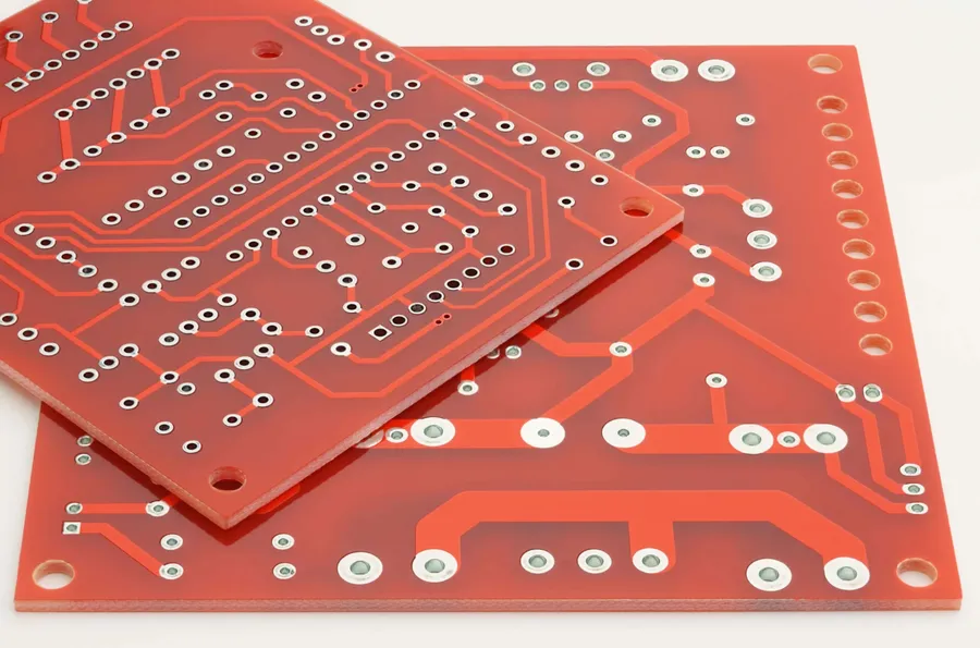
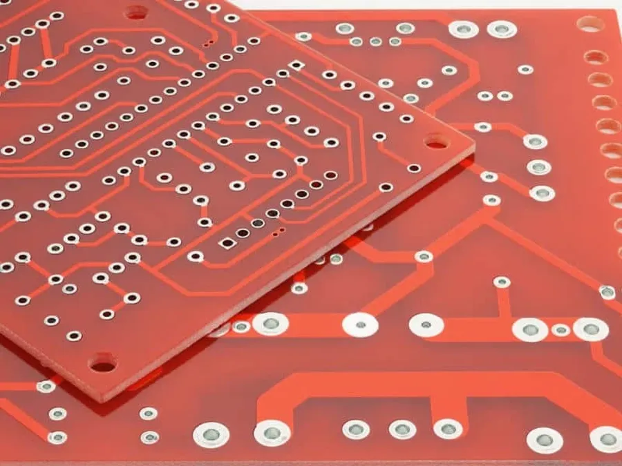
Single Layer vs. Multi-layer PCBs
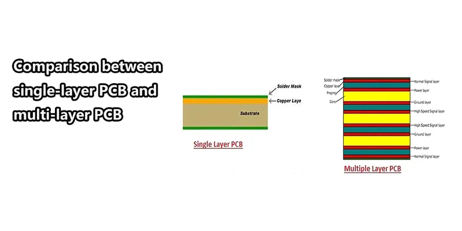
Single-layer PCBs and multi-layer PCBs represent fundamentally different approaches to circuit board design, each with its own set of advantages and limitations. The primary distinction lies in the number of conductive layers present within the board, influencing design complexity, manufacturing cost, and application suitability. Choosing the right type of PCB is crucial for optimal functionality and cost efficiency.
| Feature | Single-Layer PCB | Multi-Layer PCB |
|---|---|---|
| Number of Layers | One conductive layer | Two or more conductive layers |
| Design Complexity | Simple, less flexible routing | Complex, highly flexible routing |
| Cost | Lower cost, easier to manufacture | Higher cost, more complex fabrication |
| Component Density | Limited by single layer | Higher density possible |
| Signal Routing | Restricted, challenging with complex circuits | More routing options, suitable for complex circuits |
| EMI/RFI Shielding | Minimal shielding | Improved shielding capabilities |
| Heat Dissipation | Lower heat dissipation capability | Better heat dissipation capability due to thermal vias and copper planes |
| Typical Applications | Simple circuits, LED lighting, basic sensors | Complex electronics, high-speed applications, high-density circuits |
Applications of Single Layer PCBs
Single-layer PCBs, known for their simplicity and cost-effectiveness, find widespread use across various industries, particularly in applications where complexity is not a primary requirement. These applications range from everyday consumer goods to specialized industrial equipment, leveraging the benefits of straightforward design and manufacturing processes.
- Low-Cost Consumer Electronics
Many basic consumer devices, such as remote controls, simple toys, and basic kitchen appliances, utilize single-layer PCBs. These applications benefit from the low manufacturing cost and straightforward design associated with single-layer boards, making them ideal for mass production. - Simple Lighting Controls
LED lighting systems and basic lighting control circuits frequently employ single-layer PCBs. The low power requirements and relatively simple circuitry in many lighting applications make single-layer boards a practical and economical choice. - Basic Sensor Devices
Simple sensors, such as temperature or light sensors, often use single-layer PCBs. These boards support the integration of basic sensor components with low-complexity signal processing circuits. Applications of these sensors range from weather stations to home automation devices. - Educational Projects
Due to their simplicity, single-layer PCBs are highly favored in educational settings for teaching electronics and circuit design. Students can easily understand the layout and functionality, making them a great platform for initial learning experiences in circuit design and prototyping. - LED Lighting
Many LED lighting applications, particularly those with relatively simple lighting needs, use single-layer PCBs to support the LEDs and their associated power circuits. These include basic LED strip lighting, single-color light fixtures, and similar lighting applications. - Simple Power Circuits
Basic power regulation and distribution circuits, that do not require significant power handling capabilities, are also often built on single-layer PCBs. These could include power supplies for small devices, battery charging circuits, and low-power distribution systems.
Frequently Asked Questions About Single Layer PCBs
This section addresses common questions regarding single-layer PCBs, providing clear and concise answers based on fundamental principles and practical considerations. We aim to clarify key aspects such as cost, design methodologies, and suitability for different applications, incorporating insights from frequently asked questions.
- What exactly is a single-layer PCB?
A single-layer PCB is a type of printed circuit board that features a conductive layer, typically copper, on only one side of the insulating substrate. This design simplifies manufacturing and is suitable for less complex electronic devices, offering a cost-effective solution where high routing density isn't necessary. - How do single-layer PCBs compare to double-layer PCBs?
Single-layer PCBs have a single conductive layer, restricting routing and component placement to one side, whereas double-layer PCBs have conductive layers on both sides, offering greater design flexibility and higher component density. This difference directly impacts the complexity and capabilities of the final electronic device. Single-layer PCBs are generally simpler and cheaper to produce. - Are single-layer PCBs more cost-effective than multi-layer PCBs?
Yes, single-layer PCBs are typically the most cost-effective option. Their simplified design and manufacturing processes reduce production costs and time. This cost advantage makes them suitable for high-volume applications where complexity is not paramount. - What are the main design considerations for single-layer PCBs?
Designing single-layer PCBs requires careful consideration of trace width and spacing to avoid signal integrity issues, optimal component placement for efficient space utilization and ease of routing, and strategic via placement to reduce track complexity. The single-layer limitation necessitates a simpler and optimized approach for component interconnection. - What type of design software can be used for single-layer PCBs?
Various PCB design softwares are available that support single-layer design, including options like EasyEDA, KiCad, and Altium Designer. The choice of software often depends on the user's budget, design complexity, and familiarity with specific tools, each offering different user interfaces and functionalities. - For what applications are single-layer PCBs best suited?
Single-layer PCBs are best suited for applications that require low-complexity designs, such as simple lighting controls, basic sensor devices, educational kits, and low-cost consumer electronics. Their ease of manufacturing and cost-effectiveness make them an ideal solution for these types of devices. Additionally, simple power circuits are commonly found on single-layer PCBs. - Are there limitations to using single-layer PCBs?
Yes, single-layer PCBs have limitations, such as restricted routing capabilities due to the single conductive layer, which makes them unsuitable for complex circuits requiring intricate interconnections, and limited space for dense component placements, leading to larger board sizes for more complex functionality. They also may suffer from signal integrity issues if not carefully designed.
Future Trends and Innovations in Single Layer PCB Technology
The landscape of single-layer PCB technology is continuously evolving, driven by the ever-increasing demands for cost-effective, reliable, and versatile electronic solutions. Future advancements are focused on improving performance, expanding applications, and addressing the limitations inherent in single-layer designs.
- Advanced Materials
Research into new substrate materials, such as flexible polymers and composites, is expected to improve the mechanical properties, thermal performance, and durability of single-layer PCBs. These materials may enable new applications, such as wearable electronics and flexible displays. Conductive inks and materials also show promise in simplifying manufacturing and enabling more intricate designs. - Miniaturization and Integration
Continued miniaturization techniques will allow for higher component densities on single-layer boards. This is particularly relevant for applications where space is constrained. Integration of passive components directly onto the PCB substrate, using embedded component technology, further reduces size and improves reliability. - Improved Manufacturing Techniques
Advances in additive manufacturing, such as inkjet printing and 3D printing, offer the potential to reduce production costs and shorten manufacturing cycles for single-layer PCBs. These techniques also enable more complex and custom designs, which can be produced with greater flexibility. This will make prototyping faster and more affordable. - Enhanced Functionality
Developments in conductive adhesives and surface treatments promise to improve the reliability and performance of single-layer boards, especially in challenging environmental conditions. Improvements in signal integrity will be crucial for handling higher frequency applications. - Sustainability
As environmental concerns continue to increase, single-layer PCB manufacturing processes will likely become more sustainable. This includes a focus on developing eco-friendly materials and implementing greener production methods, such as reducing waste and energy consumption. This will reduce the overall environmental impact of single-layer PCB technology.
Single layer PCBs are the cornerstone of many electronic applications, offering an accessible entry point into electronics design and manufacturing. Understanding their design, advantages, and limitations allows engineers and enthusiasts alike to leverage their potential. While the landscape of electronics continues to grow more complex, the single layer PCB remains a crucial building block and an essential part of the electronics ecosystem.