Single Sided PCB: A Comprehensive Guide for Beginners and Professionals
In our increasingly interconnected world, single sided PCBs form the backbone of countless electronic devices, from simple toys to more sophisticated appliances. This guide dives into the specifics of single sided PCBs, offering an understanding of their construction, uses, and the crucial factors that influence their design and manufacturing, ensuring you're equipped with practical knowledge whether you're a hobbyist or an industry professional.
Understanding Single Sided PCB Structure
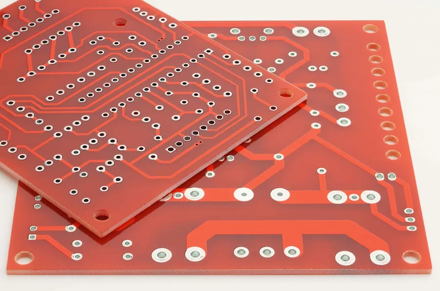
A single-sided Printed Circuit Board (PCB) is characterized by its construction, which features a conductive copper layer on one side of a substrate material. This design is fundamental to its functionality and cost-effectiveness. The primary components include the substrate, the copper layer, the solder mask, and the silkscreen. Each component serves a specific purpose in the overall performance and longevity of the board. Understanding the individual properties and the interplay between these layers is critical in PCB design.
| Layer | Material | Typical Thickness | Purpose | Key Properties |
|---|---|---|---|---|
| Substrate | FR-4 (Flame Retardant 4), CEM-1 (Composite Epoxy Material 1), Paper Phenolic | 0.8mm - 2.4mm | Provides mechanical support and electrical insulation | Rigidity, dielectric strength, thermal stability |
| Copper Layer | Copper | 18µm - 70µm | Conducts electrical signals and provides component pads | Conductivity, solderability |
| Solder Mask | Epoxy or acrylic resin | 20µm - 40µm | Protects copper from oxidation and prevents solder bridges | Insulation, chemical resistance |
| Silkscreen | Epoxy ink | Varies | Provides component markings and board information | Visibility, durability |
Key Advantages of Single Sided PCBs
Single-sided PCBs offer distinct advantages, primarily in cost-effectiveness, design simplicity, and ease of manufacturing, making them ideal for certain applications where complexity is not a necessity. These benefits stem from their straightforward construction, featuring a single conductive copper layer on one side of the substrate, simplifying the fabrication and assembly processes.
| Advantage | Description | Impact |
|---|---|---|
| Cost-Effectiveness | Reduced material usage and fewer manufacturing steps | Lower production cost, suitable for budget-sensitive projects. |
| Design Simplicity | Straightforward layout with components on one side and traces on the other | Easier to design and less prone to errors, ideal for beginners and simple applications. |
| Ease of Manufacturing | Simple fabrication process with fewer layers and no plated through holes | Faster production times, lower manufacturing costs, suitable for high-volume production of simple circuits. |
| Faster Turnaround | Quicker processing times during fabrication, including etching and component placement | Shorter lead times for prototypes and finished products, enabling faster project completion. |
| Simplified Assembly | Components placed on one side, reducing the complexity of soldering and assembly. | Easier for hand assembly or automated processes. |
Common Applications of Single Sided PCBs

Single-sided PCBs, characterized by their simplicity and cost-effectiveness, are deployed in a wide array of applications, particularly where circuit complexity is low and cost is a primary concern. Their straightforward design makes them suitable for numerous electronic devices and systems.
- Basic Consumer Electronics
Many everyday devices, such as simple calculators, remote controls, and basic kitchen appliances utilize single-sided PCBs due to their low cost and sufficient functionality for these applications. The simplicity of the circuits in these devices means complex wiring and multi-layered boards are unnecessary. - LED Lighting
Single-sided PCBs are extensively used in LED lighting applications, including light strips, indicators, and basic lighting fixtures. The straightforward nature of these circuits makes single-sided PCBs an economical and practical solution for illuminating various environments. - Simple Control Circuits
In applications requiring simple control functions, such as basic motor controls, relay boards, and timing circuits, single-sided PCBs are often the preferred choice. These circuits often do not require complex routing or high-density component placement, making single-sided PCBs ideal. - Sensor Boards
Many basic sensors, such as temperature sensors and light detectors, use single-sided PCBs because their associated circuitry is usually straightforward and doesn't necessitate the complexity of multilayer boards. These sensors typically have a small number of components which can easily be laid out on a single copper layer. - Educational Kits
Single-sided PCBs are widely used in educational kits and hobby electronics. The ease of assembly and simplicity of the design make them perfect for beginners learning about electronics and circuit design. These kits may include basic circuits such as timers, simple amplifiers, or light controllers.
| Application | Complexity | Cost | Typical Components |
|---|---|---|---|
| Basic Consumer Electronics | Low | Low | Resistors, capacitors, simple ICs |
| LED Lighting | Low | Low | LEDs, current-limiting resistors |
| Simple Control Circuits | Low to Medium | Low to Medium | Relays, switches, basic microcontrollers |
| Sensor Boards | Low | Low | Sensors, operational amplifiers |
| Educational Kits | Low | Low | Various components for simple circuits |
Single Sided PCB Design Considerations

Effective single-sided PCB design balances functionality with manufacturing constraints. This section outlines key design considerations to ensure optimal performance, manufacturability, and cost-effectiveness. Attention to trace width, component placement, and the strategic use of wire links are essential for a successful design.
- Trace Width and Spacing
Trace width must be adequate to carry the required current without excessive heat generation. Spacing between traces should adhere to manufacturing guidelines to prevent shorts. Wider traces offer lower resistance but consume more board space. - Component Placement
Optimal component placement minimizes trace length and signal interference. Group related components close together and place heat-generating components to allow for adequate thermal dissipation. Consider the ease of soldering and testing when placing components. - Via and Wire Links
Since single-sided PCBs only have one conductive layer, wire links may be necessary to connect traces that cannot directly cross. Strategically planning wire links is crucial for simplifying the design and avoiding routing conflicts. Minimize the number of wire links by optimizing placement and using creative routing techniques. - Thermal Management
Even though single-sided PCBs are often used in low-power applications, consider thermal management for components that generate heat. Heatsinks or larger copper areas can aid in dissipating heat. - Design for Manufacturability (DFM)
Adhere to the manufacturer's specifications and design rules, including minimum trace widths, spacing, and hole sizes. This ensures the design is producible and reduces the risk of manufacturing defects.
| Design Parameter | Consideration | Impact on Design |
|---|---|---|
| Trace Width | Current carrying capacity, desired impedance | Determines heat generation and signal integrity |
| Trace Spacing | Manufacturing tolerances, voltage levels | Prevents shorts and ensures electrical isolation |
| Component Placement | Signal routing efficiency, thermal dissipation, ease of assembly | Reduces signal noise, improves reliability, lowers manufacturing costs |
| Wire Links | Route paths that cannot be crossed on a single layer | Adds to assembly cost and complexity; use them judiciously |
Single Sided PCB Manufacturing Process
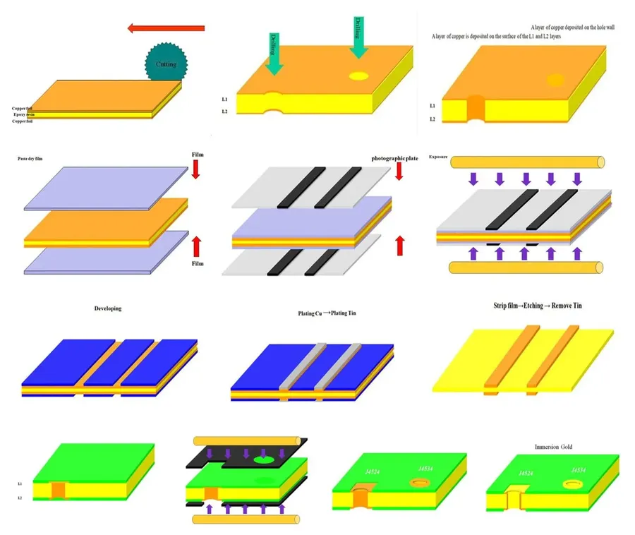
The manufacturing of single-sided PCBs is a well-defined process, crucial for producing reliable electronic circuits. This process involves a sequence of steps, starting with raw material preparation and culminating in rigorous quality checks to ensure the final product meets specifications. Each step is critical to the performance and longevity of the PCB.
- Material Preparation
The process begins with selecting the appropriate substrate material, often a rigid laminate such as FR-4 (a fiberglass-reinforced epoxy). This base material is cut to the required panel size, serving as the foundation for the PCB. - Copper Cladding
A thin layer of copper foil is laminated onto one side of the substrate. The thickness of the copper, usually specified in ounces per square foot, is chosen based on the current-carrying requirements of the application. Typical values are 1oz or 2oz. - Image Transfer
The circuit pattern is transferred to the copper layer through a photolithographic process. The PCB panel is coated with a photosensitive resist, and a film containing the circuit layout is placed over it. When exposed to UV light, the resist hardens in the areas not covered by the film, while the covered resist remains soluble. - Etching
The unexposed resist is removed, and the copper is then etched away using a chemical etchant, such as ferric chloride, from the areas not protected by the hardened resist. This results in the desired circuit pattern on the board. - Resist Stripping
The remaining hardened resist is then removed using a chemical stripper, leaving only the copper traces representing the circuit. - Solder Mask Application
A solder mask, typically a liquid epoxy, is applied over the board, except where solder pads are located. This protects the traces and prevents solder bridges during assembly. Similar to the etching process, the solder mask is applied and then cured using UV light. - Silkscreen Application
A silkscreen is printed onto the solder mask layer, usually consisting of reference designators, component symbols, and other labels. These markings facilitate component placement during assembly and identification later. - Final Curing and Finishing
The PCB is then fully cured to ensure the solder mask and silkscreen are durable and resistant to handling and environmental conditions. After this, the PCB can be routed (cut from panel) and then cleaned and inspected. - Quality Checks
The final boards undergo rigorous visual inspection and electrical testing to ensure the circuit connections are correct and meet performance requirements. Dimensional checks and further visual inspection are conducted to verify dimensional accuracy of the finished product and overall quality before delivery.
Single Sided PCB vs. Double Sided PCB: A Comparative Analysis
A critical decision in PCB design involves selecting between single-sided and double-sided boards. This choice hinges on factors such as circuit complexity, cost constraints, and application-specific requirements. While single-sided PCBs offer simplicity and affordability, double-sided PCBs provide greater routing flexibility and component density, making the selection process crucial for optimal design outcomes.
| Feature | Single Sided PCB | Double Sided PCB |
|---|---|---|
| Number of Copper Layers | One | Two |
| Routing Complexity | Limited | Higher |
| Component Density | Lower | Higher |
| Cost | Lower | Higher |
| Manufacturing Difficulty | Easier | More complex |
| Via Usage | Not applicable | Commonly used |
| Typical Applications | Simple electronics, LEDs | Complex circuits, advanced electronics |
| Design Complexity | Simpler | More Complex |
Single-sided PCBs are characterized by having all conductive traces on one side of the board, limiting the complexity of circuits they can support. Double-sided PCBs, in contrast, feature conductive layers on both sides, connected by vias, enabling more intricate circuit designs and higher component densities. Consequently, single-sided boards are often more cost-effective due to their simpler manufacturing requirements.
Choosing between single and double-sided PCBs requires a thorough evaluation of project needs. Single-sided PCBs are ideal for straightforward applications, where simplicity and cost-efficiency are paramount. However, when faced with intricate designs or more functionality within a constrained space, double-sided PCBs provide the needed flexibility, albeit at a higher cost.
Frequently Asked Questions About Single Sided PCBs
This section addresses common queries regarding single-sided PCBs, clarifying their nature, distinctions from other PCB types, and inherent limitations. We delve into topics such as the differentiation between single and double-sided protoboards and the drawbacks associated with single-sided PCBs.
- What is a single-sided PCB?
A single-sided PCB is a printed circuit board where the conductive copper traces are present on only one side of the insulating substrate. Components are typically mounted on the opposite side of the board and connected to the traces via through-hole or surface mount soldering techniques. This basic design is often the most cost-effective solution for simple electronic circuits. - How do single-sided PCBs differ from double-sided PCBs?
The primary difference is the presence of copper traces on both sides of the substrate in double-sided PCBs, enabling more complex circuitry and higher component density. Single-sided PCBs are more straightforward, with traces on only one side, making them easier and cheaper to manufacture but limiting design complexity. - What are the main limitations of single-sided PCBs?
Single-sided PCBs have limitations in circuit complexity due to the single conductive layer. This can restrict routing options and component density, potentially leading to larger board sizes and the need for wire jumpers for more intricate circuits. They also tend to have a higher susceptibility to electromagnetic interference compared to multi-layered designs, and are not suitable for high-density applications. - What is the difference between single and double-sided protoboards?
A protoboard, also known as a breadboard or perfboard, is a prototyping platform with pre-drilled holes for easy component placement. Single-sided protoboards have conductive pads on only one side, typically interconnected in a grid. Double-sided protoboards have conductive pads on both sides, often with vias connecting the two sides. This allows for more versatile circuit prototyping compared to standard single-sided PCBs, which are custom-designed for a specific application and don't typically have a grid layout. - What are the disadvantages of using single-sided PCBs?
The main disadvantages of single-sided PCBs include limited design complexity, which can increase the board size and restrict circuit routing. More advanced designs will require many wire jumpers to connect different traces, which increases cost, complexity and also increases the chance of failure. Additionally, single-sided PCBs may not be suitable for high-frequency applications due to the increased vulnerability to electromagnetic interference. - Are single-sided PCBs still commonly used in modern electronics?
Yes, single-sided PCBs are still widely used in many applications where complexity and high-performance aren't primary requirements, these include but not limited to basic consumer electronics, LED lighting, low-power control circuits, toys, and simple sensor boards. Their cost-effectiveness and simplicity in design make them a practical choice for less demanding applications. - Can single-sided PCBs be used for high-frequency applications?
While possible, using single-sided PCBs for high-frequency applications is generally not recommended. The lack of a ground plane on the opposite side can lead to increased electromagnetic interference, signal degradation, and unpredictable circuit behavior. This is due to the greater distance between the signal and return path, which is critical for signal integrity, and ultimately they are not the optimum choice for RF circuits.
Actionable Tips for Working with Single Sided PCBs
Optimizing the use of single-sided PCBs involves careful planning and execution, focusing on design, material choices, and efficient collaboration with manufacturers. This section provides actionable advice to ensure both efficiency and cost-effectiveness in your projects.
- Design Optimization for Single-Sided PCBs
Prioritize component placement to minimize trace lengths and avoid unnecessary routing complexity. Utilize wire links strategically to jump over traces, simplifying layouts and reducing the risk of shorts. Keep trace widths consistent and appropriate for the current they need to carry, avoiding thin traces which can lead to signal degradation or overheating. - Material Selection for Cost and Performance
Choose substrate materials wisely based on the application requirements. FR-4 is a common choice for its balance of cost and performance, but for more specialized applications, consider materials with specific thermal or electrical properties. Optimize copper thickness based on the current requirements to avoid over-specifying and incurring unnecessary costs. - Effective Manufacturer Communication and Collaboration
Maintain open and clear communication with your PCB manufacturer. Provide all necessary design files and specifications in a standardized format. When possible, discuss any potential design challenges or manufacturing constraints with the manufacturer beforehand to prevent costly mistakes. Request a prototype run to ensure the board meets your requirements before scaling to large quantities. - Cost Optimization
Minimize board size and complexity, this is the most effective way to reduce cost. When possible, use standard component packages to reduce assembly costs and complexity. For single-sided boards, consider using manual assembly for low quantity prototypes or specialized low quantity runs, to reduce the setup costs involved with more complex assembly methods. - Prototyping and Testing
Always prototype your design before committing to large-scale production. Test your prototypes thoroughly in the intended application and be open to iterative refinement of the design. Validate that the board’s electrical and mechanical performance conforms to the expected values and conditions.
Future Trends in Single Sided PCB Technology
While single-sided PCBs might seem like a mature technology, ongoing advancements continue to refine their capabilities and expand their applications. The future of single-sided PCBs is shaped by innovations in materials, manufacturing processes, and emerging application domains, potentially making them even more relevant in the evolving electronics landscape.
The following areas will likely see the most significant developments:
- Advanced Substrate Materials:
Research into new substrate materials with improved electrical, thermal, and mechanical properties is ongoing. This includes flexible substrates for bendable electronics and bio-based materials for more sustainable manufacturing. Such materials will enable single-sided PCBs to operate in more demanding environments and applications. - Enhanced Conductive Inks:
The development of highly conductive inks opens doors for printed electronics on flexible single-sided PCBs. This includes nano-materials for creating fine-line circuitry and printed components, paving the way for faster production and lower material costs. These advances help to reduce the need for the etching process, minimizing waste, and optimizing resource use. - Improved Manufacturing Techniques:
Innovations in manufacturing processes, such as laser direct structuring (LDS) and more precise pick-and-place technologies, are enabling the production of high-density, single-sided PCBs with greater accuracy and efficiency. Automated processes reduce errors and increase the manufacturing output. - Integration with IoT Devices:
As the Internet of Things (IoT) continues to grow, the need for low-cost, efficient PCBs for sensor nodes and basic communication devices is rising. Single-sided PCBs are uniquely positioned to serve these applications due to their simplicity and low cost, making them ideal for low-power and single-function devices. - Sustainable Practices:
There's a push for eco-friendly PCB manufacturing. This includes using recyclable materials, waterless etching methods, and reducing waste. Single-sided PCBs, due to their simpler construction, lend themselves well to these practices.
Single sided PCBs, while simple in design, are vital components in a vast array of electronic devices. Understanding their structure, benefits, design, and manufacturing processes empowers both beginners and experienced professionals to leverage their cost-effectiveness and versatility. As technology evolves, single sided PCBs will continue to play a crucial role, especially in less complex electronic devices. By focusing on efficient design and understanding their limitations, users can unlock their full potential, bridging basic functionality and cost efficiency across various fields.