The Ultimate Guide to Blank PCBs: From Basics to Applications
Have you ever wondered what lies beneath the complex circuits in your favorite gadgets? The answer often starts with a seemingly simple component: the blank PCB. These unassuming boards, the very canvas for electronic innovation, are crucial in bringing our digital world to life. This article will take you on a journey into the world of blank PCBs, unveiling their secrets, applications, and everything you need to know, acting as your comprehensive guide.
What is a Blank PCB?
A blank PCB, often referred to as a bare or empty PCB, serves as the fundamental building block for electronic circuits. It is a substrate, typically composed of fiberglass, with a layer of copper foil bonded to one or both sides. Critically, a blank PCB is devoid of any electronic components, providing a clean and flexible starting point for circuit design.
Types of Blank PCBs
Blank PCBs are categorized based on their conductive layer configuration, primarily into single-sided, double-sided, and multilayer boards. Each type caters to varying complexities and design requirements in electronic circuit construction.
| Type | Description | Typical Applications | Complexity | Cost |
|---|---|---|---|---|
| Single-Sided | Copper layer on one side of the substrate. | Simple circuits, educational projects, basic consumer electronics. | Low | Lowest |
| Double-Sided | Copper layers on both sides of the substrate, allowing for more complex routing. | Intermediate circuits, breakout boards, general-purpose electronics. | Medium | Moderate |
| Multilayer | Multiple layers of copper and substrate, enabling high-density routing. | Advanced electronics, high-speed circuits, complex digital devices, aerospace, military equipment. | High | Highest |
The selection of PCB type is pivotal for any project, depending on the circuit complexity, density needs, and budgetary constraints, with the application intended usage driving design considerations.
Materials Used in Blank PCBs
The selection of materials in blank PCBs significantly impacts their performance, durability, and application suitability. These materials primarily consist of a substrate, which provides structural support and electrical insulation, and a conductive layer, usually copper, which forms the circuit traces. Different material combinations offer varying trade-offs between cost, electrical properties, and thermal resistance.
| Material | Description | Typical Applications | Advantages | Disadvantages |
|---|---|---|---|---|
| FR-4 | Fiberglass reinforced epoxy laminate, the most common material. | General-purpose PCBs, consumer electronics, prototyping. | Good balance of cost, performance, and durability. Widely available. | Moderate heat resistance, can delaminate under extreme thermal stress. |
| CEM-1 | Paper-based composite material with a layer of woven glass fiber. | Single-sided PCBs, less demanding applications. | Cost-effective, easy to process. | Lower mechanical strength and heat resistance compared to FR-4. Not suitable for high-density circuits. |
| Metal Core PCBs (MCPCB) | Metal base (typically aluminum or copper) with a dielectric layer. | High-power applications, LED lighting, thermal management. | Excellent thermal conductivity, effective heat dissipation. | Higher cost, heavier than other materials. |
| Polyimide | Flexible material, offers high temperature resistance and flexibility. | Flexible circuits, high-temperature applications, aerospace. | High flexibility, excellent thermal and chemical resistance. | Higher cost and more complex processing compared to FR-4. |
- FR-4 (Fiberglass Reinforced Epoxy Laminate)
This is the most widely used material for PCBs due to its balanced properties. It offers good electrical insulation, mechanical strength, and is relatively cost-effective. FR-4's flame retardant properties make it a safe choice for many applications. The key characteristics are its dielectric constant, which affects signal speed, and its glass transition temperature (Tg), which determines how well it tolerates heat. - CEM-1 (Composite Epoxy Material)
CEM-1 is a paper-based composite material reinforced with a layer of woven glass fiber. It is less expensive than FR-4 but has lower mechanical and thermal performance. It is often used in single-sided PCBs for less demanding applications. - Metal Core PCBs (MCPCB)
Metal core PCBs use a metal base, usually aluminum or copper, to provide superior heat dissipation. These boards are ideal for high-power applications where heat management is crucial. The metal core is typically coated with a dielectric layer on which the copper circuitry is etched. - Polyimide
Polyimide is a flexible polymer that offers high temperature resistance, flexibility, and good chemical resistance. It is used in flexible circuits and high-performance applications where material flexibility and high temperature stability are needed.
Common Sizes and Dimensions of Blank PCBs
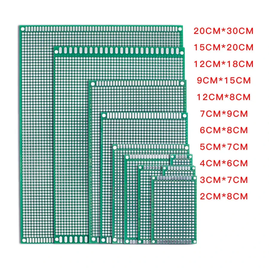
Blank PCBs are manufactured in a variety of standard sizes and custom dimensions to accommodate a wide spectrum of electronic applications. Standard sizes offer cost-effectiveness for common projects, while custom options are essential for specialized designs requiring unique board shapes and dimensions.
| Standard Size | Dimensions (Inches) | Dimensions (mm) | Typical Applications |
|---|---|---|---|
| Small Prototype | 2 x 2, 2 x 3 | 50 x 50, 50 x 75 | Simple circuits, component testing |
| Common Prototyping | 4 x 5 | 100 x 125 | General purpose circuits, medium complexity designs |
| Mid-Size Projects | 5 x 8 | 125 x 200 | Medium-sized circuits, more complex designs |
| Large Projects | 8 x 10, 12 x 12 | 200 x 250, 300 x 300 | Larger complex designs, multi-component boards |
In addition to the standard sizes, many suppliers also offer custom cutting services, allowing for the creation of boards that precisely match the user's specific needs. For prototyping, small PCBs such as 5x7 cm are common.
When selecting the appropriate PCB size, it's crucial to account for the physical dimensions of all components, the necessary spacing between traces and components, and the overall packaging requirements of the project. Proper sizing is essential for efficient production and functional performance of the end product.
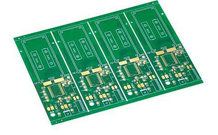
The Manufacturing Process of Blank PCBs
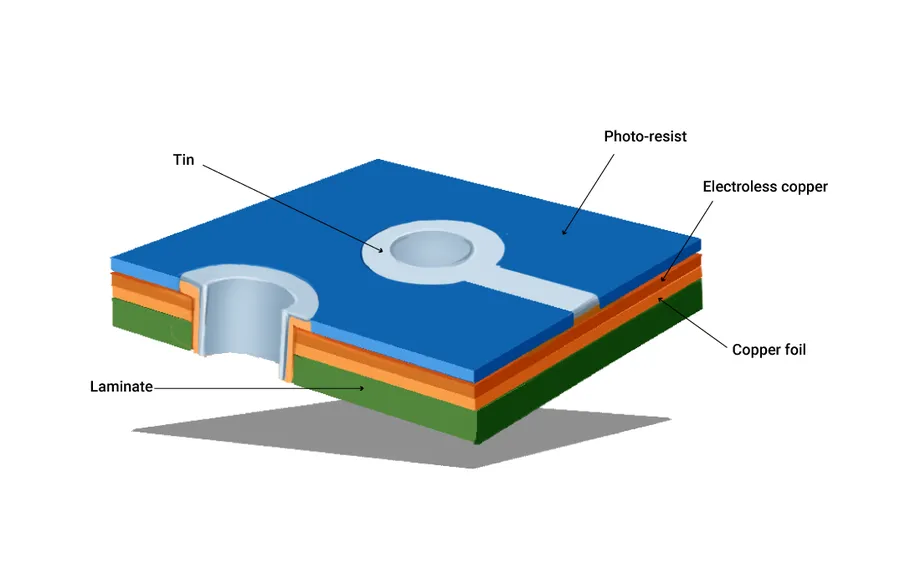
The creation of a blank PCB, the foundation for all electronic circuits, involves a sequence of precise manufacturing steps. These steps transform raw materials into the basic structure ready for component mounting. This process is critical, influencing the board's performance, reliability, and the precision of the final electronic device.
- Substrate Preparation
The process begins with selecting the appropriate substrate material, most commonly FR-4. This material is cut to the desired dimensions, forming the base of the PCB. Precision cutting ensures uniform board sizes and consistency. - Copper Lamination
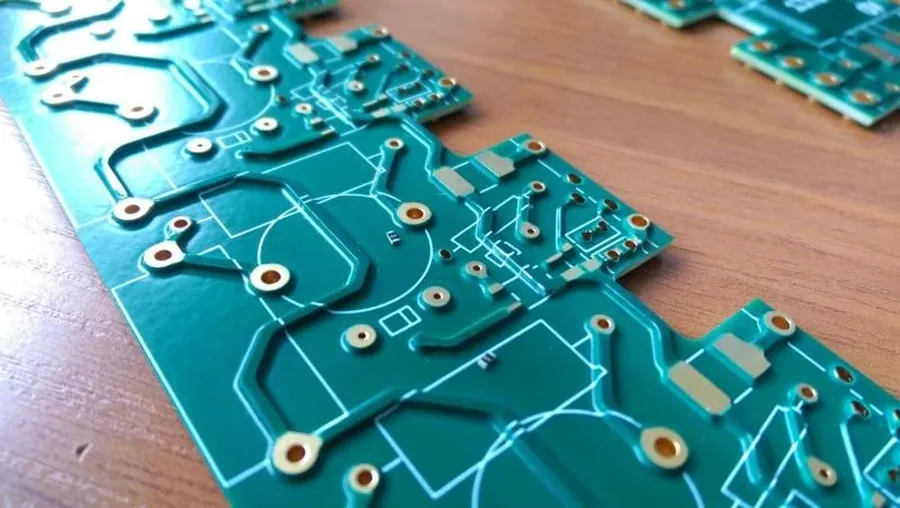
A thin layer of copper foil is then laminated onto one or both sides of the substrate using heat and pressure. This copper layer provides the conductive pathways for electrical signals. - Etching Process
The copper-clad board is then coated with a photosensitive material, which is exposed to ultraviolet light through a mask depicting the desired circuit pattern. The exposed areas harden, while the unexposed areas are washed away. A chemical etchant then removes the unwanted copper, leaving behind the precise copper traces and pads of the circuit design. - Drilling
Drilling machines are then used to create holes for component leads and vias. These holes are essential for mounting components and creating electrical connections between different layers of the board. - Surface Treatment and Quality Control
The final steps include applying surface finishes, such as solder mask (a protective layer that prevents solder bridges) and silkscreen (for component markings). Finally, each board undergoes rigorous inspection to ensure that it meets the required quality standards before being prepared for shipping.
Where to Buy Blank PCBs
Sourcing blank PCBs is a critical step in electronics prototyping and manufacturing. A variety of options are available, catering to different project needs, from small-scale hobbyist endeavors to large-scale industrial applications. Understanding the landscape of suppliers is crucial for obtaining the right boards at the right price.
- Online Retailers
Platforms like Amazon and AliExpress offer a wide selection of blank PCBs, often at competitive prices. These are suitable for hobbyists and small projects. However, ensure to check supplier reliability and product quality. - Specialized Electronics Suppliers
Companies like Jameco, Digi-Key, and Mouser Electronics specialize in electronic components, including blank PCBs. They typically provide a higher level of quality and a broader range of options, including various materials and thicknesses, often with more detailed product specifications. This is a good choice when technical specifications are of higher importance. - Direct Manufacturers
For large quantities or highly customized PCBs, consider working directly with manufacturers. This can offer cost savings at scale and provides the greatest control over material selection and design specifications, allowing more complex boards. For specific requirements, this is often the most suitable path. - Local Electronics Stores
Local electronics stores might carry a limited selection of common blank PCB sizes and materials, suitable for simple projects and prototyping. Availability can be very variable, but these can be a good option to purchase immediately, especially for beginners.
| Supplier Type | Pros | Cons | Best Use Cases |
|---|---|---|---|
| Online Retailers | Competitive pricing, wide selection, convenient shopping | Variable quality, potential for unreliable suppliers | Hobbyists, small-scale projects, prototyping |
| Specialized Suppliers | Higher quality, broader selection of materials, detailed product specifications | Potentially higher prices, may require minimum order quantities | Technical projects, professional development, specific material requirements |
| Direct Manufacturers | Cost savings at scale, full customization, precise control over specifications | Requires large quantities, longer lead times, requires technical knowledge | Large-scale projects, industrial applications, complex designs |
| Local Electronics Stores | Immediate availability, suitable for simple projects, accessibility | Limited selection, potentially higher prices, may not have specific types | Simple prototyping, quick access, beginners |
DIY and Custom PCB Creation
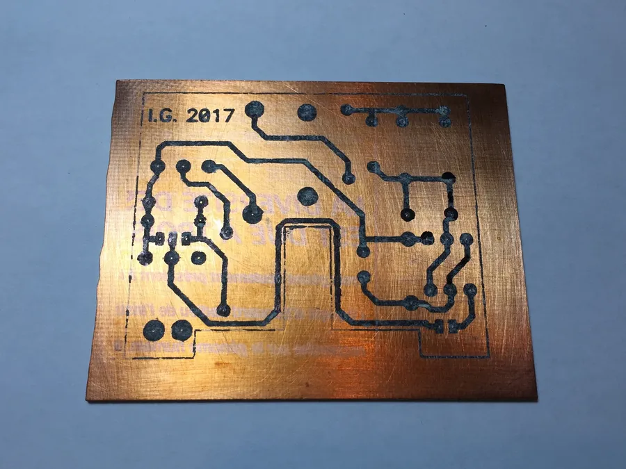
For advanced users and hobbyists, creating custom blank PCBs in-house provides unparalleled flexibility and deepens understanding of the fabrication process. This approach allows for highly customized layouts, unique board shapes, and sizes not readily available through standard suppliers.
There are two primary methods for creating custom PCBs: chemical etching and CNC milling, each with distinct advantages and requirements.
- Chemical Etching
This method involves printing the desired circuit pattern onto a copper-clad board using a laser printer and toner transfer paper. The board is then immersed in an etchant solution, typically ferric chloride, which dissolves the exposed copper, leaving the desired circuit traces intact. This process requires safety precautions due to the chemicals involved, including proper ventilation and personal protective equipment. - CNC Milling
CNC milling uses a specialized machine with a small milling bit to physically remove copper from the PCB, thereby defining the traces and pads. This method does not involve chemicals, but it does necessitate a CNC milling machine capable of high precision and a proper CAM (Computer-Aided Manufacturing) software to generate toolpaths from the PCB design files.
Both methods offer the advantage of creating custom-sized and shaped boards, which can be useful for non-standard enclosures or applications. The DIY approach is beneficial for rapid prototyping of new designs and for gaining a deeper understanding of the PCB fabrication process.
Frequently Asked Questions About Blank PCBs
This section addresses common queries regarding blank PCBs, offering clear and concise answers to help users better understand these fundamental components of electronics manufacturing.
- What are blank PCBs also called?
Blank PCBs are also commonly referred to as bare PCBs or empty PCBs. These terms all describe a printed circuit board that has not yet had any electronic components attached. - Why can PCBs sometimes be expensive?
The cost of PCBs can vary significantly based on several factors. These include the size of the board, the number of layers (single, double, or multi-layer), the materials used (such as FR-4, CEM-1, or metal cores), and the precision required in the manufacturing process. Complex designs or special material requirements can substantially increase costs. - What is a zero PCB board?
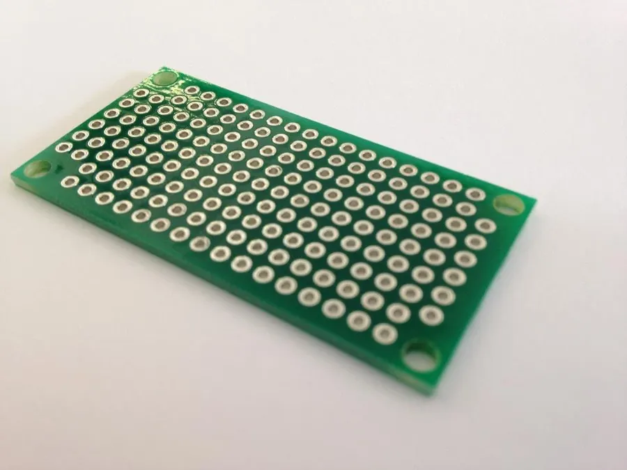
A 'zero PCB board' is a term often used to describe a prototyping board, typically with a grid of pre-drilled holes. These boards are designed for the easy assembly of through-hole components without the need for custom etching, enabling hobbyists and engineers to quickly prototype basic circuits. It's essentially a blank canvas for building experimental electronics. - What does 'blank circuit' mean in the context of PCBs?
A 'blank circuit' in the context of PCBs refers to the state of the board before any electrical circuit is formed. It's the initial condition of a blank PCB where conductive pathways are present but not yet interconnected to function as a specific electronic circuit. - Can I make my own blank PCBs?
Yes, it is possible for advanced users to make their own blank PCBs. Common methods include using a laser printer and chemical etchants to transfer a circuit pattern onto a copper-clad board, or utilizing a CNC milling machine to remove unwanted copper. This requires specific tools, materials, and expertise in PCB design and fabrication. - How does the number of layers affect the blank PCB's cost?
The number of layers significantly influences the cost of a blank PCB. Single-sided boards are the least expensive, while double-sided and multilayer boards increase in cost due to the more complex fabrication processes and materials required for their production. Multilayer PCBs allow for higher circuit density and more complex designs, which justifies the additional expense in many applications.
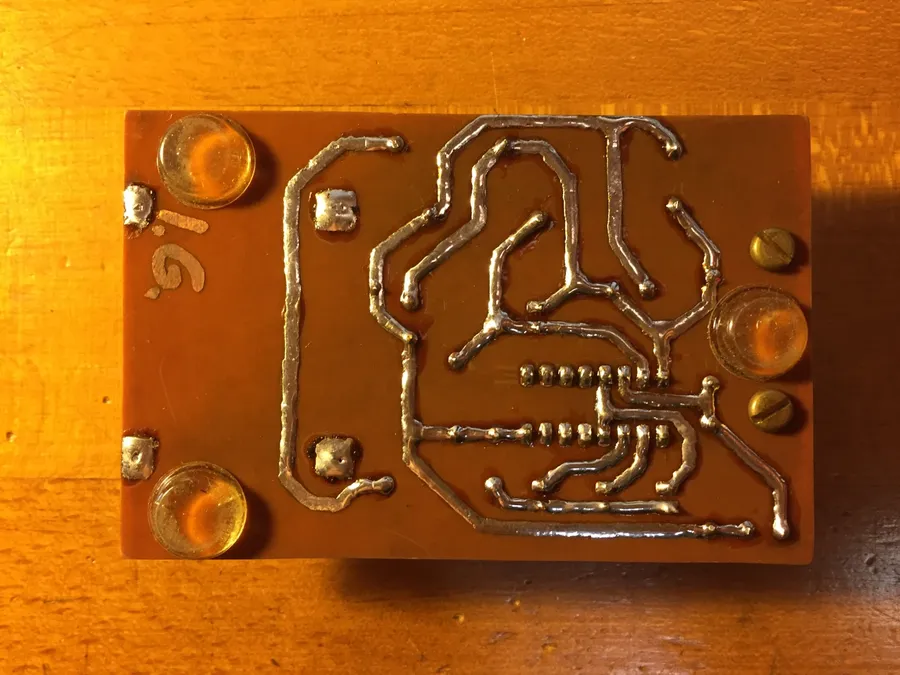
Using Blank PCBs: Tips and Best Practices
Working with blank PCBs requires careful planning and execution to ensure the creation of functional and reliable electronic circuits. This section outlines essential tips and best practices for handling, designing, and assembling components onto blank PCBs, emphasizing precautions to prevent damage and ensure optimal performance.
- Handling Precautions
Always handle blank PCBs by the edges to avoid transferring oils and contaminants from your fingers to the copper traces, which can interfere with soldering and conductivity. Additionally, be aware of electrostatic discharge (ESD) risks; use proper grounding techniques and ESD-safe tools to protect sensitive components from damage. - Design Considerations
Utilize PCB design software to plan and verify the circuit layout before beginning assembly. Carefully consider trace width, spacing, and component placement for proper signal transmission and heat dissipation. Ensure the design adheres to your specific needs and adheres to standard design rules. - Proper Soldering Techniques
Use a temperature-controlled soldering iron to avoid overheating the PCB and components, which can lead to damage. Use the correct solder type and flux to ensure quality connections. Always ensure adequate ventilation to avoid inhaling solder fumes, and practice soldering on scrap boards first to get the process down before attempting it on the actual project. - Component Placement
Plan the order in which you will solder components to ensure that you're not blocking access to other parts of the circuit. Start with smaller, less critical components before moving on to larger, heat-sensitive ones. Pre-tinning component leads and pads can help to ensure proper solder flow during the final soldering step. - Testing and Verification
Thoroughly test the assembled PCB using a multimeter to verify that there are no shorts or open circuits. Validate power and signal paths to ensure the circuit functions as designed. Troubleshoot and rectify any identified issues before moving on. This is a vital step to avoid potential damage or failure down the road.
Blank PCBs vs. Pre-Etched Boards
The selection between blank PCBs and pre-etched boards hinges on project requirements, particularly concerning complexity, customization needs, and user expertise. Blank PCBs provide a versatile foundation for intricate and custom circuit designs, acting as a blank canvas. Pre-etched boards, while offering convenience for simpler designs, compromise flexibility for complex projects, often making them suitable for simple circuits or as a starting point for novice users.
Blank PCBs, the silent heroes of electronics, form the base upon which countless innovations are built. Understanding the ins and outs of these bare boards is essential for anyone involved in electronics, whether you’re a hobbyist, a student, or a professional engineer. With the right knowledge and planning, a blank pcb can be transformed into a functional and efficient circuit, limited only by your imagination and goals. As we advance in technology, the blank PCB will remain at the forefront of electronic advancements, making the world of electronics accessible to everyone.