The Ultimate Guide to Copper PCB Boards: Materials, Types, and Applications
In our daily lives, copper plays a pivotal role, silently enabling much of the technology we rely on. From the complex circuits in our smartphones to the robust systems in industrial machines, the copper PCB board is the unsung hero. This article explores the world of copper PCB boards, detailing their composition, manufacturing, varied types, and critical role in modern electronics, helping you understand this fundamental component.
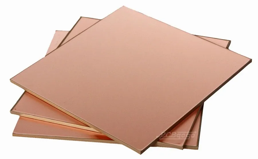
Understanding Copper Clad Laminates
Copper clad laminates (CCLs) are the foundational building blocks of printed circuit boards (PCBs). They are composite materials comprising a base substrate, typically a non-conductive material, and a thin layer of copper foil bonded to one or both sides. The precise arrangement of these layers is paramount to the performance and functionality of the resulting PCB.
The selection of the base substrate, such as FR-4, significantly influences the laminate's mechanical and electrical properties, while the copper foil's thickness and quality determine the board's conductivity and current-carrying capacity. This interplay of materials dictates the PCB's ultimate suitability for specific electronic applications.
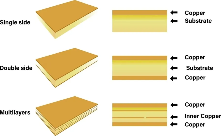
Single-Sided vs. Double-Sided Copper PCB Boards
Single-sided and double-sided copper PCB boards represent fundamental configurations in circuit board design, each offering distinct advantages and limitations that determine their suitability for various electronic applications. Understanding these differences is crucial for engineers and designers selecting the appropriate board type.
| Feature | Single-Sided PCB | Double-Sided PCB |
|---|---|---|
| Copper Layers | One layer of copper on one side of the substrate | Two layers of copper on both sides of the substrate |
| Complexity | Simpler design, fewer routing options | More complex designs, greater routing flexibility, ability to create more connections. |
| Via Usage | No vias are typically used as there is only one copper layer | Vias are used to create interconnections between the top and bottom layers. |
| Cost | Generally less expensive to manufacture | More expensive to manufacture. |
| Applications | Suitable for simpler circuits, low-density applications such as LED lighting, simple sensors, and basic control circuits | Suitable for complex circuits, higher density applications such as communication devices, computer hardware, and industrial control systems. |
The choice between single-sided and double-sided PCBs hinges on the complexity and functional requirements of the electronic device. Single-sided boards are cost-effective for basic circuits where routing is straightforward, whereas double-sided boards provide the necessary flexibility for intricate designs. The manufacturing process for double-sided PCBs is more involved, including additional steps to ensure proper alignment and interconnection between the copper layers. The vias are a critical part of double sided boards, creating pathways to connect components on either side. Understanding the routing limitations of single sided boards and benefits of vias in double sided boards helps engineers select the right type of board for their project
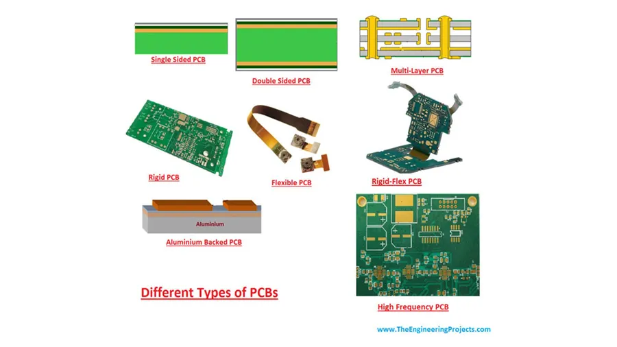
Types of Copper PCB Boards Based on Materials
The performance and application of a copper PCB board are significantly influenced by the base material used in its construction. Common materials include FR-4, phenolic, and others, each offering distinct properties that cater to different design and performance requirements. Understanding these materials is crucial for selecting the appropriate PCB for a given application.
| Material | Description | Thermal Stability | Cost | Typical Applications |
|---|---|---|---|---|
| FR-4 | Flame Retardant 4, a composite material made of woven fiberglass cloth with an epoxy resin binder. | Good | Moderate | General-purpose PCBs, widely used in various applications |
| Phenolic | Paper-based material impregnated with phenolic resin. | Lower | Low | Lower-cost consumer electronics, simpler circuits |
| CEM-1 | Composite material made of paper and woven glass fabric with epoxy resin binder. | Moderate | Moderate | General-purpose PCBs where cost is a consideration |
| Aluminum | Aluminum substrate with a dielectric layer and copper foil. | Excellent | Higher | LED lighting, power electronics, applications requiring efficient heat dissipation |
| Polyimide | Flexible polymer material that provides high temperature resistance and flexibility | High | High | Aerospace, medical equipment, high-frequency applications, flexible circuits |
Copper Thickness in PCBs: What You Need to Know
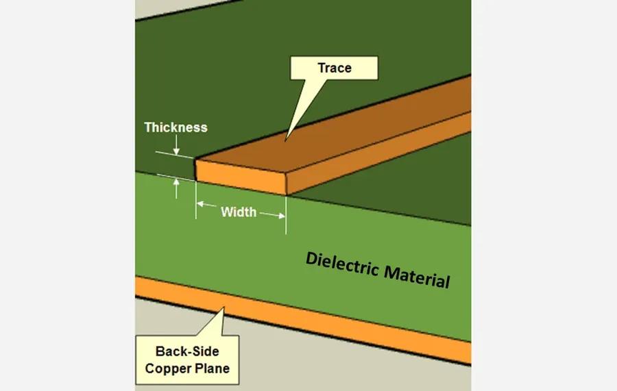
Copper thickness in printed circuit boards (PCBs), typically measured in ounces (oz), is a critical parameter influencing both the electrical performance and the structural integrity of the board. The weight of copper spread over one square foot defines the thickness, where 1 oz copper corresponds to approximately 1.37 mils (0.0348 mm) or 34.8 micrometers. Understanding copper thickness is crucial for managing current-carrying capacity, signal integrity, and overall PCB reliability.
| Copper Thickness (oz) | Approximate Thickness (mils) | Approximate Thickness (mm) | Applications |
|---|---|---|---|
| 0.5 oz | 0.70 | 0.0174 | Low power, signal layers |
| 1 oz | 1.37 | 0.0348 | General purpose, standard applications |
| 2 oz | 2.74 | 0.0696 | Moderate power, power layers |
| 3 oz | 4.11 | 0.1044 | Higher power, heavy current applications |
| 4 oz and above | 5.48+ | 0.1392+ | High power, demanding environments |
Thicker copper layers allow for higher current carrying capacity, which is essential for power electronics. However, increased copper thickness can affect the etching process, making it more challenging to create fine traces and leading to increased cost. Conversely, thinner copper layers are easier to process and are suitable for signal layers with low power requirements, but they are more susceptible to signal loss and have limited current carrying capacity. The choice of copper thickness depends greatly on the specific application requirements and board design considerations.
The Manufacturing Process of Copper PCB Boards
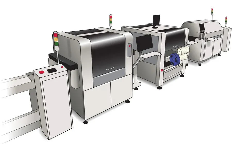
The fabrication of copper PCB boards involves a series of precise and controlled steps, transforming raw materials into functional circuit boards. This process encompasses everything from the initial design to the final board testing, with each stage playing a critical role in determining the board's performance and reliability.
Here's a breakdown of the key steps involved:
- Design and Layout
The process begins with the design of the circuit board using CAD (Computer-Aided Design) software. This stage involves defining the placement of components, the routing of traces (conductive paths), and the overall board dimensions. The design also specifies the type of copper thickness required and any other special considerations such as impedance control. - Printing the Circuit Pattern
The designed circuit pattern is transferred onto a transparent film or a photo-plotter. This film is used to create a mask for subsequent etching processes. - Preparing the Copper Clad Laminate
A copper clad laminate, consisting of a base material (like FR-4) with a thin layer of copper foil bonded to one or both sides, is prepared. The laminate is cleaned to ensure proper adhesion of the photoresist. - Applying the Photoresist
A layer of photosensitive material (photoresist) is applied to the copper surface. This material hardens when exposed to UV light. - Exposure and Development
The photoresist-coated laminate is exposed to UV light through the mask. The UV light hardens the photoresist according to the circuit pattern. The unexposed photoresist is then removed in a developing solution, revealing the copper that needs to be etched away. - Etching
The exposed copper is removed by chemical etching, leaving only the desired circuit traces. Common etchants include ferric chloride or cupric chloride. - Resist Removal
Once etching is complete, the remaining photoresist is removed, revealing the copper circuit pattern. - Drilling and Plating
Holes are drilled for component leads and vias (connecting layers). For multilayer PCBs, this is a key stage for vias through the stacked layers. In multilayer boards, the drilled holes are then plated with copper (electroless plating, followed by electrolytic plating) to establish electrical connectivity between layers. - Solder Mask Application
A solder mask is applied to the board to protect the copper traces from oxidation and to prevent solder bridging during assembly. It also provides a surface for silkscreen printing. - Silkscreen Printing
Silkscreen printing is used to apply identifying markers, component outlines, and logos to the board for easier assembly and troubleshooting. - Surface Finishing
The boards undergo surface finishing to enhance solderability and protect the copper. Common finishes include HASL (Hot Air Solder Leveling), ENIG (Electroless Nickel Immersion Gold), and OSP (Organic Solderability Preservative). - Electrical Testing
Finally, the fabricated PCBs undergo electrical testing to verify the circuit's integrity. This includes testing for shorts, opens, and the correctness of electrical parameters. - Profiling/Routing
The individual boards are cut out from the production panel by routing or v-scoring. The v-score is used when the boards will be separated later in the assembly process.
Each of these stages requires careful control of process parameters, such as temperature, chemical concentration, and exposure times. Maintaining this accuracy is crucial for producing high-quality and reliable copper PCB boards.
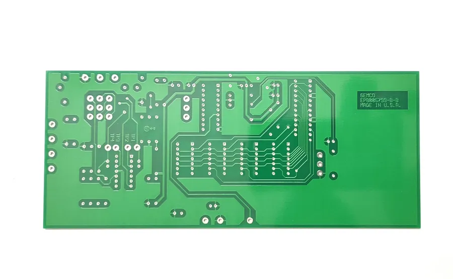
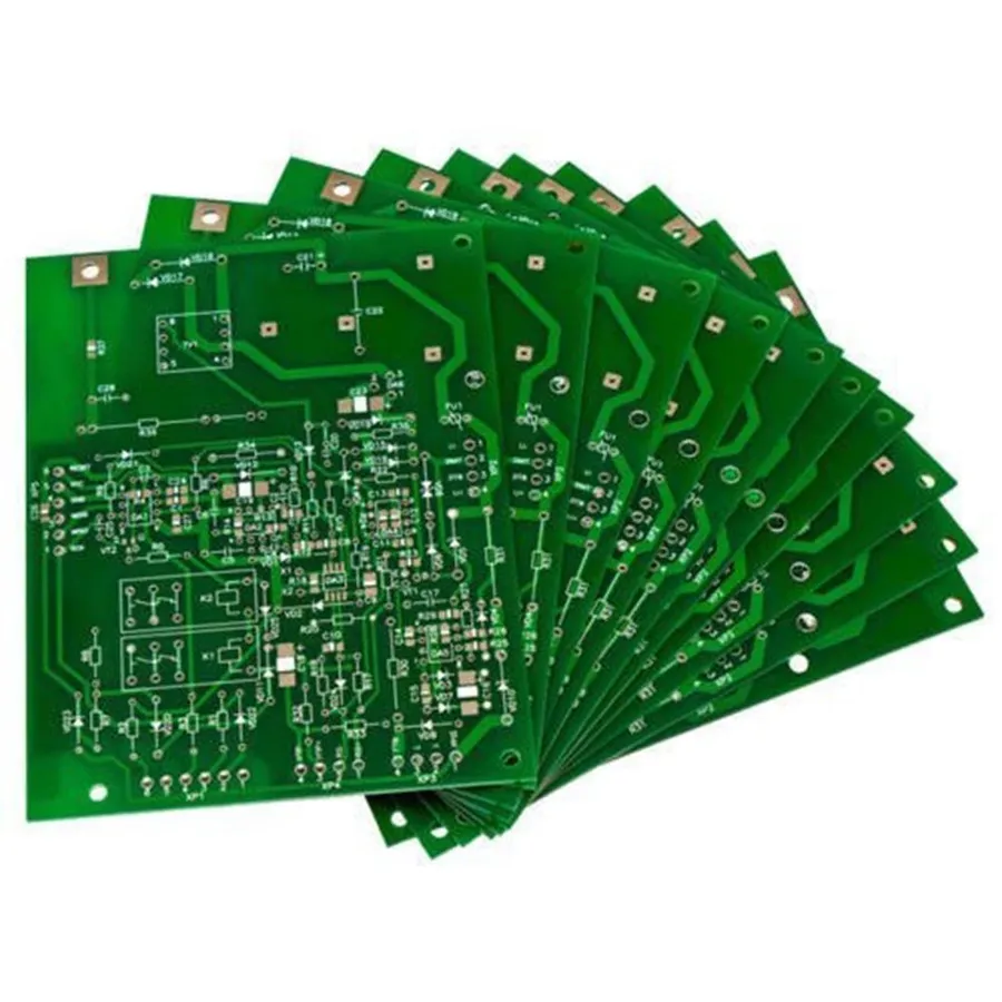
Applications of Copper PCB Boards
Copper PCB boards are fundamental components in a vast array of electronic devices, serving as the backbone for electrical connections and component mounting. Their versatility and conductive properties make them indispensable across diverse sectors, from everyday consumer electronics to highly specialized aerospace applications.
- Consumer Electronics
Copper PCB boards are ubiquitously used in smartphones, tablets, laptops, and home appliances. They facilitate the complex circuitry required for these devices to operate efficiently. - Telecommunications
In telecommunications, copper PCBs are critical for networking equipment such as routers, switches, and base stations, enabling reliable and high-speed data transmission. - Automotive Industry
Modern vehicles heavily rely on copper PCBs for engine control units (ECUs), infotainment systems, safety features like ABS and airbags, and various sensors. These boards must endure harsh conditions, necessitating robust design and materials. - Industrial Equipment
Industrial machinery, control systems, and automated equipment incorporate copper PCBs to manage complex operations and ensure reliable performance in demanding environments. They are also common in power conversion and distribution systems. - Medical Devices
From diagnostic equipment to patient monitoring devices and implantable technologies, copper PCB boards play a vital role in healthcare. Their reliability and precision are critical for accurate diagnoses and effective treatments. - Aerospace and Defense
In aerospace and defense, copper PCBs are found in navigation systems, communication arrays, and control systems for aircraft, satellites, and missiles. The need for high reliability and resistance to extreme conditions is paramount in these applications. - LED Lighting
Copper PCBs provide both the electrical connections and thermal management necessary for LED lighting applications, including household, commercial, and outdoor lighting systems.
Frequently Asked Questions About Copper PCB Boards
This section addresses common inquiries regarding copper PCB boards, providing clear and concise answers to help you better understand their composition, usage, and properties.
- What exactly is a copper PCB board?
A copper PCB (Printed Circuit Board) board is a foundational component in electronics, consisting of a non-conductive substrate (like FR-4) layered with conductive copper traces. These copper traces form the electrical pathways that connect various electronic components mounted on the board, enabling the functionality of electronic devices. The copper provides excellent conductivity, crucial for signal transmission and power distribution. - What are copper clad boards primarily used for?
Copper clad boards, which are essentially PCBs before components are mounted, serve as the base for constructing electronic circuits. They are the canvas upon which circuits are designed by etching away unwanted copper, leaving the desired conductive pathways. These boards are used in nearly all electronic devices for mounting components, providing mechanical support, and facilitating electrical connections. - How can copper be recovered from a PCB board?
Recovering copper from PCB boards is a multi-stage process typically involving physical and chemical methods. Initially, components are removed and the boards are often shredded. The shredded material then undergoes processes like hydrometallurgy (using chemical leaching to dissolve copper), or pyrometallurgy (high-temperature smelting), to separate the copper from other metals and non-metallic materials. The recovered copper can then be refined and reused, contributing to a circular economy and reducing reliance on virgin materials. However, these are complex industrial scale processes. - How thick is a 1 oz copper PCB layer?
A 1 oz copper PCB layer, often referenced in PCB specifications, corresponds to a copper thickness of approximately 1.37 mils (thousandths of an inch), or 0.0348 mm. The '1 oz' designation indicates that one ounce of copper, spread evenly over a one-square-foot area, would achieve this specific thickness. This unit is crucial in PCB design, dictating the current-carrying capacity and signal integrity of the traces. - Can a copper clad board be used for other purposes beyond electronics?
While primarily designed for electronics, copper clad boards, due to their unique material properties, can be repurposed for other applications, such as art projects involving conductive surfaces, model making where electrical contacts are required, or for scientific experimentation involving controlled electrical pathways. However, alternative materials may be more suitable for non-electrical applications depending on requirements. - What is the significance of copper purity in PCB boards?
The purity of copper in PCB boards is critical to its performance. High purity copper offers superior electrical conductivity, reduced signal loss, and better heat dissipation. Impurities in copper can lead to increased resistance, affecting the efficiency and reliability of the circuit. Therefore, PCB manufacturers use high-grade copper to ensure optimal performance and long-term stability of the electronic devices that rely on these boards. - Is it possible to repair a copper PCB board at home?
While minor repairs like soldering a broken trace or replacing a component are possible with appropriate tools and skill, more extensive damage is often unrepairable. Home repairs should be undertaken only with proper safety precautions, as soldering involves heat and potentially toxic fumes. For complex issues, professional repair or replacement may be more suitable and reliable.
Comparing Copper PCB Boards: Phenolic vs FR4
Selecting the appropriate base material for a copper PCB is critical to its performance and longevity. Phenolic and FR4 are two common materials, each possessing distinct properties that suit different applications. This section provides a detailed comparison to guide informed material selection.
| Feature | Phenolic PCB | FR4 PCB |
|---|---|---|
| Material Composition | Paper impregnated with phenolic resin | Woven fiberglass cloth impregnated with epoxy resin |
| Cost | Lower | Higher |
| Thermal Stability | Lower, prone to warping at higher temperatures | Higher, more resistant to temperature fluctuations |
| Mechanical Strength | Lower, more brittle | Higher, more durable and less prone to cracking |
| Moisture Resistance | Lower, absorbs moisture, affecting performance | Higher, better resistance to humidity |
| Electrical Properties | Adequate for basic circuits | Superior, consistent dielectric constant |
| Fire Resistance | Lower, more flammable | Higher, self-extinguishing |
| Applications | Simple, low-cost electronics, hobbyist projects | Most electronics, high-performance applications, reliable operation |
| Workability | Easy to cut, drill, and handle | Requires more robust tools due to fiberglass |
In summary, Phenolic PCBs are cost-effective and suitable for basic, low-temperature applications. However, FR4 PCBs offer superior mechanical strength, temperature resistance, and electrical characteristics making it the preferred choice for most applications that require high reliability and performance. When selecting materials consider cost, operating environment, and required electrical performance to align with the specific needs of your project.
Practical Tips for Working with Copper PCB Boards
Working with copper PCB boards, whether for hobbyist projects or professional applications, requires a blend of careful design, precise fabrication, and meticulous soldering techniques. This section provides actionable advice to help you navigate these stages effectively, minimize errors, and ensure the successful creation of robust and reliable circuit boards. We cover everything from design considerations to best practices for handling copper clad materials during the etching and soldering phases.
- Designing for Copper PCBs
Start with a well-defined schematic. Use PCB design software to accurately translate the schematic into a layout. Pay close attention to trace width, spacing, and component placement to ensure electrical functionality and manufacturability. Always check design rule compliance (DRC) to avoid errors like short circuits or insufficient clearances. - Choosing the Right Copper Clad Material
Selecting the appropriate copper clad laminate is crucial. For most general purpose applications, FR4 is the most suitable choice. However, consider other materials like phenolic for more budget-friendly boards, or materials with better high-frequency performance characteristics if needed. Consider the thickness of the copper clad, as it determines the current carrying capability. One-ounce copper is often a default option for standard circuits, but higher current designs may need 2 oz or even 3 oz copper to ensure it can handle the current demands. - Etching Best Practices
When etching, ensure you have the appropriate etchant (e.g., ferric chloride or ammonium persulfate), and follow proper safety procedures. Consistent agitation and temperature control of the etchant are vital for uniform etching. Use a toner transfer method or photoresist process to achieve precise etching patterns from your design. Always check that the etching process removes all the unnecessary copper from the board to avoid shorts. - Soldering Techniques
Employ proper soldering techniques. Ensure the soldering iron is at the correct temperature, and use flux to help solder flow properly. Apply solder to pads rather than the component leads to improve the connection. Avoid overheating components which can damage them. Always double check the soldering joints to ensure there are no dry joints. - Handling Copper Clad Materials
Handle copper clad materials with care to avoid scratches and contamination. Store boards in a dry environment to prevent oxidation. Use gloves to prevent skin oils from interfering with the etching process and the soldering. Use non-scratching cleaning solutions or microfibers to clean boards to avoid damaging the copper surface. - Common Errors to Avoid
Be meticulous with your layouts, as common errors include short circuits due to lack of clearance, poorly designed vias that cause connection issues, not having enough copper for sufficient current flow, and poor solder joints due to bad soldering practices. Carefully plan the board design to avoid such issues. Before etching, double check the board for any flaws in the toner transfer or photoresist. Test your boards thoroughly before integrating them into a finished product. This allows for easy corrections before problems become more difficult to solve. - Recommended Tools
Essential tools include a precision soldering iron with temperature control, good quality solder, desoldering wick, flux, a multi meter, a well vented area for soldering and etching, personal protective equipment and a sharp cutting tool. You will also need copper clad materials, etching chemicals, photoresist or laser printer for toner transfer, and a PCB design software package.
Copper PCB boards are a cornerstone of modern electronics, underpinning countless devices that enhance our lives. Understanding their composition, types, and applications provides valuable insights into the technology around us. As technology advances, the role of the copper PCB board will remain pivotal in innovation. By learning how these components are made and used, designers can optimize their electronic designs and unlock the potential of copper in future advancements.