Top 3D Printed Circuit Board Companies: Revolutionizing Electronics Manufacturing

From the smartphones in our hands to the complex systems powering industries, electronics underpin modern life. The traditional way of producing circuit boards is now being challenged by a fascinating technology: 3D printing. This article will dive deep into the world of 3D printed circuit board companies, exploring how they are reshaping electronics manufacturing, offering faster prototyping, and pushing the boundaries of what's possible in additive manufacturing.
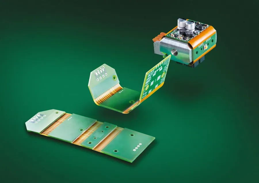
The Rise of 3D Printed Circuit Boards
The integration of 3D printing into circuit board manufacturing marks a significant shift, driven by the demand for rapid prototyping, intricate designs, and customized electronics. This innovative approach transcends the constraints of conventional PCB production, enabling engineers and designers to realize concepts previously deemed unfeasible, and is seeing increasing adoption across a range of industries.
Several key factors have contributed to the increasing adoption of 3D printing in PCB manufacturing:
- Reduced Lead Times:
Traditional PCB manufacturing often involves lengthy processes, while 3D printing enables rapid prototyping and production, significantly reducing the time from design to functional circuit board. - Design Flexibility:
3D printing allows for the creation of complex geometries and intricate designs that are difficult or impossible to achieve with conventional methods, providing greater flexibility in electronic design. - Customization:
The ability to produce highly customized circuit boards tailored to specific applications with relative ease is a key advantage, especially for niche or low-volume electronics production. - On-Demand Manufacturing:
3D printing offers on-demand production capabilities, allowing for more efficient manufacturing workflows and cost savings, especially for low-volume production. - Complex Geometries:
With layer-by-layer construction, 3D printing excels at creating intricate, multi-layered circuits, something that is challenging for traditional PCB fabrication methods.
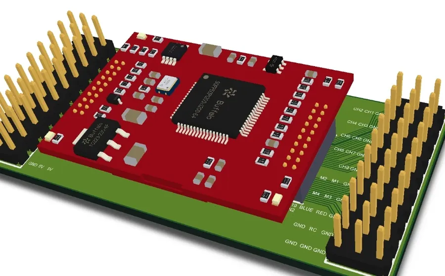
Key Players in 3D PCB Printing

The 3D printed circuit board market is rapidly evolving, with several companies pioneering advanced technologies and carving out distinct market positions. These key players are driving innovation in materials, printing methods, and application development. This section highlights some of the most influential companies in the 3D PCB printing space.
- Nano Dimension
Nano Dimension is renowned for its DragonFly Pro system, which utilizes inkjet technology for multi-layer PCB fabrication. Their focus is on rapid prototyping and agile hardware development, enabling companies to quickly iterate on designs with high precision. They are recognized for their ability to produce complex circuits, including embedded components and through-hole vias, in a single printing process. - BotFactory
BotFactory offers the Squink system, a desktop solution for PCB prototyping and functional electronics manufacturing. Their technology combines material dispensing and pick-and-place capabilities, facilitating the creation of diverse electronic circuits. BotFactory emphasizes ease of use and accessibility, making 3D PCB printing more available to a wider audience, including smaller design firms and academic institutions. - Neotech AMT
Neotech AMT specializes in 3D printed electronics using its unique Aerosol Jet technology for conformal and embedded electronics. Their method is effective for creating complex geometries and integrating electronics directly onto 3D structures, making it suitable for aerospace, automotive, and medical device applications. Neotech AMT's offerings emphasize high precision and advanced material capabilities. - IDS (Innovative Digital Systems GmbH)
IDS focuses on additive manufacturing solutions for printed electronics, leveraging technologies suitable for a range of PCB designs. They are known for their flexibility in supporting various substrate materials and conductive inks, enabling rapid prototyping as well as customized production requirements. IDS works on solutions for rapid development cycles and quick-turn production of 3D printed PCBs. - Optomec
Optomec is a leader in Aerosol Jet printing, which is utilized in various fields including printed electronics. Their systems allow for the direct printing of electronic circuits onto complex and non-planar substrates, suitable for applications requiring high flexibility and performance in harsh environments. They offer printing solutions to various electronic manufacturing challenges.
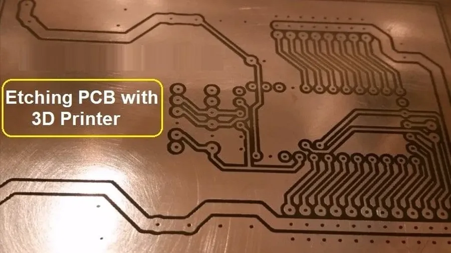
Understanding Different 3D PCB Printing Technologies
The landscape of 3D printed circuit board (PCB) manufacturing is defined by a variety of technologies, each with unique capabilities and limitations. Understanding these methods is crucial for selecting the appropriate approach for specific applications. This section details the primary 3D printing techniques used in PCB fabrication, including their operational principles and suitability for different PCB requirements.
| Technology | Description | Strengths | Weaknesses | Material Compatibility | Typical Application |
|---|---|---|---|---|---|
| Aerosol Jet Printing | Uses a carrier gas to deposit conductive inks or other materials onto a substrate. The material is sprayed in a fine mist and then dried or cured to form the desired pattern. | High-resolution printing, wide material compatibility, non-contact process. | Limited layer thickness, requires specialized inks, can be slower than other methods. | Conductive inks, polymers, ceramics, nanoparticles. | High-precision circuits, sensors, antennas, flexible electronics. |
| Material Jetting | Employs print heads to precisely deposit droplets of photopolymer resins which are then cured using UV light. Multiple print heads are able to deposit multiple materials simultaneously. Can build complex structures. | High-resolution printing, excellent surface finish, allows for multi-material deposition. | Can be costly, limited material selection, can require support structures. | Photopolymer resins. | Prototyping, complex structures, multi-layer PCBs. |
| Fused Deposition Modeling (FDM) | Extrudes a thermoplastic filament through a heated nozzle to build the desired structure layer by layer. | Cost-effective, suitable for larger parts, simpler technology. | Limited resolution, typically used for non-functional prototypes, poor conductivity. | Thermoplastic polymers embedded with conductive particles | Early stage prototyping, basic structural components, limited electronic functionality. |
| Direct Ink Writing (DIW) | Uses a nozzle to dispense viscous inks (conductive or dielectric) onto a substrate. These inks can be pastes, gels or other viscous materials that maintain shape after dispensing. | Versatile material selection, can handle highly viscous materials, high print volumes. | Print resolution can be limited by nozzle diameter, requires controlled environment for optimal printing, needs specific viscosity inks. | Conductive pastes, polymers, ceramics, epoxies. | Large area electronics, sensors, flexible circuits |
Comparing 3D PCB Printing vs. Traditional PCB Manufacturing
3D printed circuit boards and traditional PCBs represent distinct manufacturing approaches, each with unique advantages and limitations. A direct comparison highlights the trade-offs between these methods across key factors such as cost, speed, materials, design flexibility, and production volume.
| Feature | 3D Printed PCBs | Traditional PCBs |
|---|---|---|
| Cost | Higher for small volumes, lower for complex designs and prototypes. Tooling costs can be avoided. | Lower for high-volume production, but higher initial setup costs and tooling for complex designs. |
| Speed | Faster turnaround for prototypes and custom designs, with minimal lead times. | Longer lead times, especially for complex designs and initial setup. |
| Materials | Limited by printable conductive inks and substrates, expanding but still less diverse than traditional methods | Wider range of materials and substrate options, including FR-4, Rogers, and flexible substrates. |
| Design Flexibility | Excellent for complex geometries, multi-layer structures, and custom designs. | Limited by subtractive manufacturing processes, more difficult to achieve complex internal geometries. |
| Production Volume | Best suited for low to medium volume production, prototyping, and customized parts. | Ideal for high-volume manufacturing due to established processes. |
| Layer Count | Potentially higher layer count capability, with vertical interconnects readily achievable. | Limited layer count, with more complex structures requiring specific, costly processes. |
| Environmental Impact | Potentially less waste from additive process, reduced chemical use. | Significant waste from subtractive processes and use of chemicals |
Materials Used in 3D Printed Circuit Boards
The selection of materials is paramount in 3D printed circuit board (PCB) manufacturing, directly influencing the functionality, performance, and durability of the final product. These materials must exhibit specific electrical and mechanical properties to ensure optimal operation in diverse applications. This section will explore the key materials employed in 3D PCB printing, including conductive inks, polymers, and ceramics, and will emphasize the importance of appropriate material selection.
| Material Type | Description | Typical Applications | Advantages | Disadvantages |
|---|---|---|---|---|
| Conductive Inks | Inks containing conductive particles (e.g., silver, copper, gold) dispersed in a carrier fluid. | Creating conductive traces, interconnects, and components in circuits. | High conductivity, fine feature resolution, flexible substrate compatibility. | Potential for oxidation, material cost, limited structural integrity. |
| Polymers | Thermoplastics and thermosets, often used as the substrate material or for encapsulation. | Structural support, insulation, encasing sensitive components. | Wide range of mechanical properties, cost-effective, good flexibility. | Limited thermal stability, potential for moisture absorption, lower electrical conductivity |
| Ceramics | Inorganic, non-metallic materials offering high thermal and electrical stability. | High-temperature applications, components requiring high dielectric strength. | Exceptional thermal and chemical resistance, high dielectric strength. | Brittle, more expensive, limited flexibility. |
The choice of material is contingent on the specific application requirements. For instance, flexible electronics necessitate the use of flexible conductive inks and polymers, whereas high-temperature applications demand ceramics. Furthermore, material compatibility with the printing process itself (Aerosol Jet, Material Jetting, or Fused Deposition Modeling) is an important factor to consider for optimal printing results and to ensure the final product meets the desired performance metrics.
Applications of 3D Printed PCBs
3D printed circuit boards (PCBs) are rapidly expanding beyond prototyping, finding diverse applications across various industries due to their unique capabilities in creating custom and complex electronic components. The flexibility of 3D printing allows for innovative solutions in fields where traditional manufacturing methods fall short.
- Rapid Prototyping
3D printing enables engineers to quickly produce and test PCB prototypes, dramatically reducing lead times and facilitating faster design iterations, which is crucial for agile development cycles. - Custom Electronics
The ability to create uniquely shaped and sized PCBs makes 3D printing ideal for custom electronic devices and systems where standard boards will not fit or meet the specific requirements, including wearables, sensors, and specialized robotics. - Aerospace
In the aerospace sector, 3D printed PCBs can withstand extreme temperatures and vibrations, enabling the production of lightweight, high-performance components for satellites, drones, and aircraft, contributing to enhanced operational efficiency and performance. - Medical Devices
3D printing allows the fabrication of intricate, patient-specific PCBs for medical devices, including prosthetics, implants, and diagnostic tools, enhancing patient care through customized and biocompatible solutions. - Internet of Things (IoT)
The complexity of IoT devices, combined with the need for miniaturization and integration, makes 3D printing a highly suitable method for developing custom PCBs that fit the small form factors and unique requirements of various IoT applications, such as smart homes, industrial sensors, and environmental monitoring systems. - Research and Development
3D printing enables researchers to experiment with unique geometries and materials, supporting exploration into new electronic devices, and thus accelerating technological advancements.
Frequently Asked Questions About 3D Printed PCBs
This section addresses common questions regarding 3D printed circuit boards (PCBs), providing clarity on cost, turnaround time, and the future potential of this innovative technology.
- What are the primary cost factors associated with 3D printed PCBs?
The cost of 3D printed PCBs is influenced by several factors, including material costs (conductive inks, polymers), printing technology used (aerosol jetting, material jetting), design complexity, layer count, and production volume. Initial setup costs may be higher than traditional methods but can be offset by reduced material waste, faster prototyping, and the ability to produce highly customized boards. As the technology matures and materials become more readily available, costs are expected to decrease. - How does the turnaround time for 3D printed PCBs compare to traditional PCB manufacturing?
One of the major advantages of 3D printed PCBs is their significantly faster turnaround time, particularly for prototypes and small production runs. Traditional PCB manufacturing involves multiple steps and can take weeks, whereas 3D printing can produce boards in a matter of hours or days, depending on the complexity and size of the board. This rapid prototyping capability allows for faster design iteration and reduced time to market. However, this advantage may diminish for mass production runs. - Can 3D printed PCBs achieve the same level of performance as traditional PCBs?
While 3D printed PCBs are rapidly advancing, they currently may not match the high-volume performance of traditional PCBs across all parameters. For example, achieving high-frequency signal integrity or very high layer counts is an active area of development. However, 3D printed PCBs are highly suitable for many applications, and ongoing advancements in materials and printing technologies are continually expanding their performance capabilities. The best choice depends heavily on the specific application's requirements. - What types of materials are commonly used in 3D printed PCBs?
Common materials include conductive inks based on silver or copper nanoparticles, insulating polymers like polyimides or epoxies, and sometimes ceramics for specific high-temperature or high-frequency applications. The choice of material depends on the performance requirements of the PCB, including conductivity, insulation, thermal stability, and mechanical robustness. The continued development of new materials is expanding the range of applications for 3D printed PCBs. - What is the typical size and complexity of PCBs that can be produced with 3D printing?
Currently, the build volume for most 3D PCB printers limits the overall size of printed circuit boards. Typical boards are similar to those used in mobile phones and other small electronics. Complexity is less limited by the printing process itself but by design rules and the capability of the printing material to maintain fine details. However, technology is advancing to allow for larger PCBs and increasingly complex designs. - What are the primary applications where 3D printed PCBs are most beneficial?
3D printed PCBs are particularly advantageous for rapid prototyping, custom electronics, small batch production, and applications with unique or complex shapes that are difficult to produce with traditional methods. Specific sectors include aerospace, medical devices, Internet of Things (IoT) applications, and research & development environments, where the ability to quickly iterate on designs or produce specialty boards outweighs the cost for mass production. They also excel in applications requiring conformal electronics or intricate 3D structures. - What are the future possibilities for 3D printed PCBs?
The future of 3D printed PCBs is promising, with ongoing advancements in materials, printing technologies, and software. Expect to see improvements in material conductivity, mechanical strength, and thermal resistance, as well as increased printing resolution and speed. We also expect to see greater integration of 3D printing into a more digital and automated manufacturing process and in the future, the ability to print fully functional multi-layered PCBs with embedded components, all from a single 3D printing process.
Future Trends in 3D Printed Electronics
The future of 3D printed electronics is poised for significant advancements, driven by innovations in materials, automation, and software. These developments promise to revolutionize not only how circuit boards are manufactured but also how electronic devices are designed and integrated into our daily lives.
- Advancements in Materials Science
The exploration of new conductive and non-conductive materials is crucial for enhancing the performance and functionality of 3D printed electronics. Research is focused on developing materials with improved conductivity, thermal stability, and mechanical properties, including novel inks, polymers, and ceramics. - Increased Automation
The incorporation of robotics and AI is expected to automate the 3D printing process, leading to higher production rates, improved accuracy, and reduced manufacturing costs. Automated systems will also facilitate the integration of 3D printing with other manufacturing processes. - Enhanced Software Capabilities
Sophisticated software will play a critical role in the future of 3D printed electronics. Advanced design tools, simulation software, and integrated platforms will enable engineers to create more intricate and functional electronic devices with greater precision and efficiency. - Integration with AI and IoT
The integration of 3D printed electronics with artificial intelligence (AI) and the Internet of Things (IoT) will unlock new possibilities for smart devices and connected systems. 3D printing allows for the customized fabrication of sensors and actuators, leading to the creation of intelligent and personalized electronic products. - Development of Multi-Material Printing
Multi-material printing will enable the fabrication of complex electronic devices in a single build, combining conductive, insulating, and structural materials seamlessly. This technology will accelerate the creation of high-performance, miniaturized, and flexible electronics. - Sustainability and Eco-Friendly Practices
A growing emphasis on sustainable manufacturing practices is driving the adoption of eco-friendly materials and printing processes. This will involve the development of recyclable or biodegradable materials and the minimization of waste in the 3D printing of electronics.
The landscape of electronics manufacturing is rapidly changing thanks to the rise of 3D printed circuit board companies. These innovators are not just creating boards; they're crafting a future where electronic devices are more customized, more accessible, and faster to prototype and produce. The continued development of 3D PCB printing will undoubtedly lead to remarkable innovations across countless industries, and companies like Nano Dimension and BotFactory are at the forefront, paving the way for a new era of electronic possibilities.