Transform Your Arduino Project: From Breadboard to Custom PCB
The Arduino platform has revolutionized electronics prototyping, enabling rapid development of interactive projects. But what happens when you want to take your creation from a breadboard to a more robust and permanent solution? The answer lies in the Arduino PCB—a printed circuit board designed to bring your Arduino projects to life in a compact and reliable form. This article will explore the process of designing, creating, and optimizing your own custom Arduino PCB, offering a comprehensive guide for hobbyists and professionals alike.
Understanding the Need for an Arduino PCB
Transitioning from a breadboard to a custom Printed Circuit Board (PCB) for Arduino projects marks a significant step towards enhanced functionality, reliability, and professional presentation. While breadboards are invaluable for prototyping, they present limitations that a custom PCB effectively addresses, especially when projects move beyond initial experimentation.
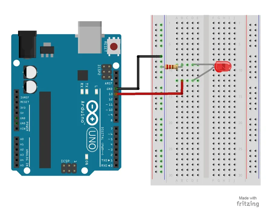
Breadboard prototypes, while excellent for initial circuit construction and testing, suffer from several drawbacks which become more apparent with increasing complexity. These limitations include a lack of physical robustness, susceptibility to loose connections which can interrupt operation, a tendency towards unwieldy layouts, and general difficulties in portability. By contrast, a custom Arduino PCB overcomes these challenges by offering a more compact, durable, and reliable solution, making it ideal for permanent installations and projects requiring greater stability.
| Feature | Breadboard Prototype | Custom Arduino PCB |
|---|---|---|
| Durability | Low, easily damaged and connections can be loose | High, robust and resistant to physical damage |
| Reliability | Prone to connection issues | Stable and consistent connections |
| Size | Often bulky and cumbersome for complex projects | Compact and can be designed to fit specific size constraints |
| Organization | Can become disorganized with many components and wires | Well-organized with clear layouts and component placements |
| Portability | Difficult to transport and use outside of a lab setting | Highly portable and suitable for long term installations and projects |
| Professionalism | Looks like a prototype | Looks finished and professional |
The shift to a custom PCB is motivated by the need for a finalized, reliable product. A custom PCB not only provides a robust platform for electronic components but also enables better thermal management, allows for optimized signal routing to minimize interference, and ultimately facilitates a more professional and refined outcome.
Planning Your Arduino PCB: Schematic Design
The schematic diagram is the foundational blueprint for any printed circuit board (PCB), and for an Arduino project, it serves as a vital link between your conceptual design and a physical realization. This design process involves representing electronic components and their interconnections using symbolic representations. A well-structured schematic not only guides the subsequent layout process, but also is crucial for accurate component selection, efficient PCB assembly, and effective troubleshooting.
A comprehensive schematic design process consists of several key steps:
- Component Selection
Carefully select components based on your project's functional requirements and ensure that they are available in surface-mount packages that are suitable for PCB assembly, such as resistors, capacitors, integrated circuits, and connectors. Consider components that are widely available to prevent future issues with supply. For an Arduino project, this might include a microcontroller, voltage regulator, and any necessary interface circuits. - Schematic Capture
Use schematic capture software to draw the circuit, connecting components with wires, also referred to as nets, and adding labels to each net for identification. This stage involves placing components onto a drawing canvas, using pre-defined symbols to represent the actual electronic parts, and connecting these symbols with wires (nets). The components must be chosen based on the application specifications. Common software options for this process are KiCad, EasyEDA, and Altium Designer. - Annotation and Validation
Label all components with appropriate reference designators and validate the schematic against your design specifications. Use the software's annotation features to assign unique identifiers to each component (e.g., R1, C2, U3) to ensure it can be referenced during assembly and troubleshooting. It's best practice to perform a design rule check (DRC) within your schematic capture software to verify that no components are missing and that there are no shorted components. Verify connections, power supply and ground connections to avoid potential errors.
Key considerations for selecting components for your Arduino PCB design:
- Component Footprint
Choose components with footprints that are suitable for PCB manufacturing, such as surface-mount (SMD) components or through-hole (THT) components that can be soldered to the board. SMD components are preferred for their smaller size and suitability for mass production, however, THT components are easier for manual assembly. - Availability
Prioritize components that are readily available from reputable suppliers, to avoid supply chain issues later during production. Consider components that are not subject to long lead times or end of life notifications. - Electrical Specifications
Ensure that each component's electrical ratings (voltage, current, power) are compatible with the operating requirements of your project, including but not limited to temperature limits. Use components that can comfortably operate within their intended limits.
PCB Design Software Options for Arduino
Selecting the right PCB design software is crucial for transforming your Arduino project from a breadboard prototype to a custom printed circuit board. This section explores several popular options, evaluating their ease of use, features, and costs, specifically considering their compatibility with Arduino projects. The goal is to empower you to choose the software that best fits your skill level and project needs, ensuring a smooth transition from schematic capture to PCB layout.
| Software | Ease of Use | Key Features | Cost | Arduino Compatibility |
|---|---|---|---|---|
| KiCad | Moderate | Open-source, Cross-platform, Full suite of tools, 3D viewer | Free | Excellent |
| EasyEDA | High | Cloud-based, Integrated with LCSC component library, Community collaboration features | Free (with paid options) | Good |
| Fritzing | High | Beginner-friendly, Breadboard view, Simple PCB layout | Free | Good for basic projects |
| Eagle | Moderate | Industry standard, Large component library, Powerful PCB layout tools | Subscription-based | Excellent |
| Altium Designer | Low | Professional-grade, Advanced features, High cost | High-cost subscription | Excellent |
The software options above offer varied approaches to PCB design. KiCad, as a completely free and open-source software, provides an excellent solution with a full suite of tools. EasyEDA's cloud-based accessibility and direct integration with a component library make it highly efficient for rapid prototyping. Fritzing is perfect for those new to PCB design due to its simplicity and breadboard simulation features. Eagle has historically been an industry standard and is quite powerful, while Altium Designer is usually preferred by professional engineers due to it's extensive features, but has a higher cost barrier to entry.
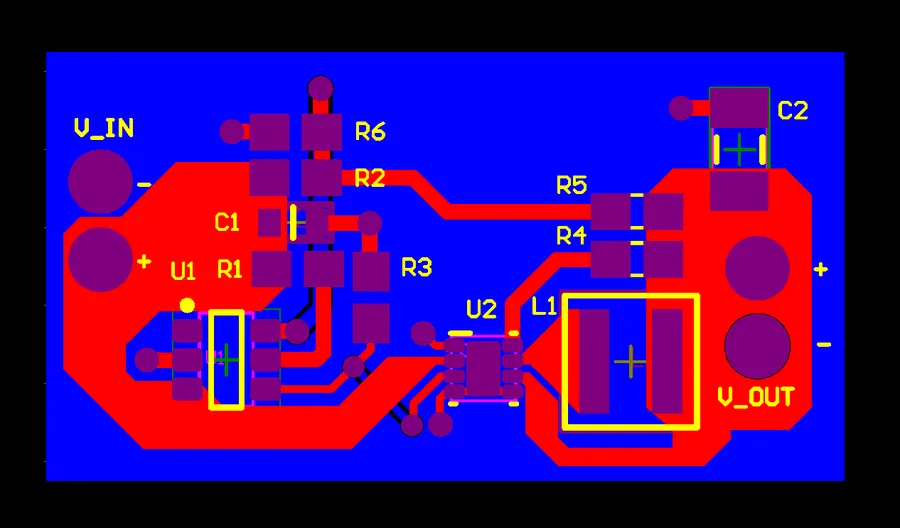
Laying Out Your Arduino PCB
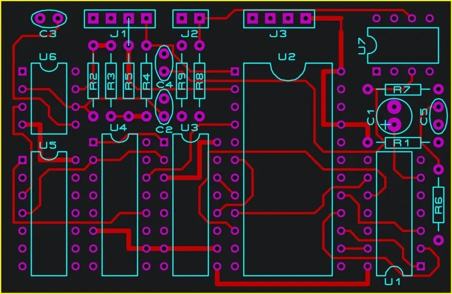
Effective PCB layout is crucial for the functionality and reliability of any Arduino-based project transitioning from a breadboard to a custom printed circuit board. This process involves the careful arrangement of electronic components, the routing of conductive traces, and consideration of thermal management and manufacturability to ensure the PCB operates as intended, with specific attention to Arduino integration.
- Component Placement
Start by strategically placing components, prioritizing the Arduino microcontroller and its related circuitry. Group components based on their functional relationships, placing critical components like power regulators and crystal oscillators close to the microcontroller. Consider the physical dimensions of each part and their footprints when determining placement. - Trace Routing
The routing of traces (copper paths connecting components) must ensure that signals travel efficiently between components. Employ techniques such as minimizing trace lengths, avoiding sharp angles which can cause signal reflection, and using appropriate trace widths for different current levels. Separate sensitive analog traces from noisy digital traces to prevent interference. - Ground Planes and Power Distribution
Implement a dedicated ground plane, usually on one of the PCB layers, to provide a stable ground reference for all components. Distribute power via sufficiently wide traces or power planes to handle the current demands of the board. Ensure bypass capacitors are placed close to the power pins of active components, such as the microcontroller, for stable voltage. - Thermal Considerations
Consider how much heat components will generate when in operation. High heat dissipation components, such as voltage regulators, should have adequate copper areas for heat transfer. Use thermal vias to conduct heat away from components and consider heatsinks where necessary, in cases where there is high power dissipation. - Manufacturability
Adhere to your selected manufacturer’s Design for Manufacturability (DFM) guidelines, including minimum trace widths and clearances, via sizes, and annular ring requirements. This will help prevent fabrication problems. Double check your design for errors and ensure it meets the manufacturing limitations. - Arduino Specific Considerations
Ensure all connections to the Arduino board or microcontroller are made correctly. Take care of signal pin assignments, power requirements, and ensure the headers are accessible for connecting external hardware if needed. The form factor of your PCB should align with your intended application and the Arduino ecosystem, or be a unique design.
From Gerber Files to Manufactured PCBs
The culmination of PCB design is the generation of Gerber files, the industry-standard format for communicating design specifications to PCB manufacturers. These files encapsulate all the necessary information, such as copper layers, solder mask, silkscreen, and drill data, required for fabrication. Subsequently, selecting a suitable manufacturing service becomes paramount, factoring in cost, turnaround time, and the complexity of your design.
The following details the process and considerations when moving from design to fabrication.
- Gerber File Generation
Gerber files are typically generated directly from your PCB design software. The process usually involves selecting a Gerber output option and choosing the specific layers needed for production, such as top and bottom copper layers, solder mask, and drill files. Most software will have a specific 'Generate Gerber' or 'Plot' option to create the necessary files. - Understanding Gerber File Formats
Different file extensions represent different layers. For example, `.GTL` might represent the top copper layer, while `.GBL` could represent the bottom copper layer, with `.GKO` being the outline of the board, etc. Each file is a text-based representation of the physical PCB layout. Always verify the outputted Gerber files using a Gerber viewer to confirm the layers are correct. - Selecting a PCB Manufacturer
Numerous PCB manufacturing services are available online, offering a range of options and pricing tiers. Consider factors like the complexity of your design (number of layers, trace width, via size), the desired quantity of boards, turnaround time, and shipping costs. Comparing multiple quotes and looking at online reviews before selecting is critical.
| Factor | Description | Considerations |
|---|---|---|
| Design Complexity | Number of layers, trace width, via size | More complex designs increase cost and potentially require more specialized manufacturers. |
| Quantity of Boards | Number of PCBs to be produced | Unit price decreases as quantity increases. |
| Turnaround Time | Time from order to delivery | Faster turnaround usually results in higher costs. |
| Cost | Price per board and additional fees | Compare multiple quotes from different manufacturers. Be wary of extremely cheap offers, as this may indicate a lower quality board. |
| Shipping | Time and cost for shipping | Factor shipping into overall cost, particularly from overseas manufacturers. |
By carefully navigating the Gerber file generation process and thoughtfully choosing a manufacturer, your Arduino PCB design will be brought from concept to reality.
Assembling and Testing Your Arduino PCB
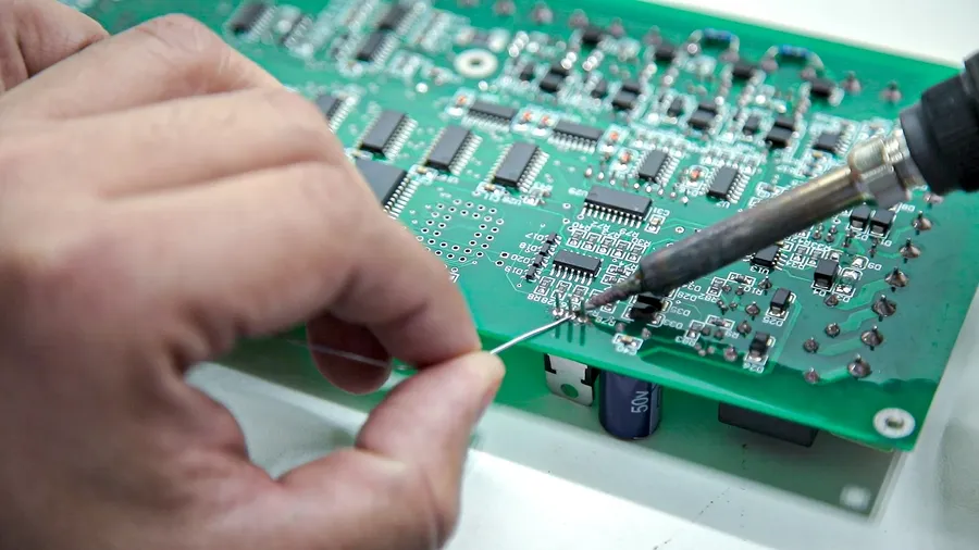
The transition from a designed PCB to a functional electronic system involves careful component assembly and thorough testing. This section details the crucial steps of soldering components onto your custom Arduino PCB, functional testing procedures, and effective troubleshooting techniques. Successfully navigating this phase is essential to validate the design and ensure its performance.
- Soldering Components
Soldering is the process of joining electronic components to the PCB using a molten metal alloy (solder). It requires precision and care. Ensure you use appropriate soldering equipment (soldering iron, solder, and flux), and follow proper soldering techniques to achieve strong and reliable connections. Begin with larger components and proceed to smaller, more delicate components, and double-check each solder joint for a good connection and avoid cold solder joints. - Essential Soldering Equipment
A temperature-controlled soldering iron with various tip sizes is necessary. Additionally, lead-free solder, flux, desoldering braid (for removing excess solder), and tweezers for handling small components are essential. It's also recommended to have a good magnifying glass and ventilation system to enhance visibility and maintain safety. - Testing Functionality
After soldering, visual inspection for poor solder joints or accidental shorts. Once satisfied with the soldering quality, connect the assembled PCB to a power source and test its basic functionality. Use a multimeter to verify voltage levels and continuity at critical points in the circuit. Start with a simplified test program or use simple diagnostic test that can quickly check essential features. - Troubleshooting Common Issues
Debugging the PCB includes checking for shorts, opens, and correct components. Incorrect component placement or faulty components are often sources of problems. Use datasheets to verify the functionality of individual components and a circuit diagram to locate test points to check for signal and power issues. Thorough troubleshooting is crucial before proceeding to the next stage of development.
Frequently Asked Questions About Arduino PCBs
This section addresses common inquiries regarding Arduino PCBs, providing clear, concise answers to guide your understanding and project development.
- What exactly is an Arduino PCB?
An Arduino PCB (Printed Circuit Board) is a custom-designed board that houses the electronic components of an Arduino project, replacing the need for a breadboard. It offers a more permanent, robust, and compact solution compared to a breadboard prototype. It typically includes the microcontroller, power regulation, and any other components specific to the application. Essentially it's a tailored physical manifestation of your electronic design. - How can I create my own Arduino PCB?
Creating your own Arduino PCB involves several key steps: First, design your schematic diagram, selecting components suitable for PCB mounting. Second, choose PCB design software to lay out your board. Third, generate Gerber files from the PCB layout. Finally, use a PCB manufacturing service to fabricate the board. Once manufactured, components are soldered, followed by rigorous testing. This process requires careful planning and attention to detail. - How many layers are typically found in an Arduino Uno PCB?
The standard Arduino Uno PCB typically utilizes a two-layer design. This means that the conductive copper traces that form the electrical connections are located on two separate layers of the board (top and bottom), simplifying both design and manufacturing. However, more complex custom PCBs can use four or more layers to accommodate more sophisticated circuitry. - How do I transition from an Arduino prototype to a production-ready PCB?
Transitioning from a prototype to a production PCB requires moving from a breadboard to a custom PCB design. This entails several considerations: optimizing the design for manufacturability (DFM), ensuring proper component selection and sourcing, selecting a manufacturing process appropriate for your production volume, testing and iteration, and finally setting up a quality control process. Planning for scalability is crucial when moving to mass production. - Is using a custom PCB always better than a breadboard for an Arduino Project?
While a custom PCB provides numerous advantages like durability and compactness, it's not always the superior choice. Breadboards are more flexible for rapid prototyping and experimentation. The decision depends on the project's complexity, production volume, and the intended use-case. Breadboards remain ideal for early-stage development and testing. - Can I use surface mount components for my Arduino PCB?
Yes, surface mount components (SMD) can be used effectively in Arduino PCBs, allowing for smaller and more compact designs. SMD components are directly mounted on the PCB surface rather than having leads through holes. The usage requires attention to correct footprint in design, and you also need to be competent in soldering SMD components, typically requiring some experience, flux, and a hot air station. This design approach is ideal for more complex, high-density boards. - What are the key factors to consider when designing a custom Arduino PCB?
Key considerations include: Component placement to optimize signal routing and minimize noise, trace width and spacing to ensure adequate current carrying capacity, thermal management to prevent overheating, via placement for layer-to-layer connections, and choosing a suitable PCB material for the environmental conditions. Also it is necessary to ensure that the design is manufacturable, also known as Design for Manufacturing (DFM).
Advanced Tips for Arduino PCB Design
Optimizing an Arduino PCB beyond basic functionality involves considering factors like power management, signal integrity, and physical size. These advanced techniques are crucial for creating robust, efficient, and production-ready designs tailored to specific applications. Addressing these aspects will move your project beyond a simple prototype to a professional, market-ready product.
- Power Management Optimization
Implementing efficient power regulation is critical, especially for battery-powered applications. This involves selecting low-dropout regulators (LDOs), considering switching regulators for higher efficiency, and incorporating power-saving modes. Careful component selection and circuit design minimize power consumption and extend battery life. - Signal Integrity Considerations
Ensuring signal integrity minimizes signal degradation and interference, particularly in high-frequency circuits. Techniques include impedance matching, proper trace routing, using ground planes, and minimizing trace lengths. Proper termination methods and shielding techniques can also significantly improve the reliability of the PCB. - Size Reduction Strategies
Reducing the size of the PCB is often essential for compact devices. Surface-mount components (SMD) are smaller than through-hole components and enable more compact designs. Careful layout and use of multi-layer PCBs also contribute to a smaller footprint. Integrating functions into fewer components is also an option by using integrated circuits with multiple function blocks. - Design for Manufacturing (DFM)
Creating a PCB that is easily assembled and tested in a production environment is necessary. Design choices like component orientation, test points placement, and panelization are important. Adhering to design rules provided by manufacturers reduces errors and production costs. Consulting with your PCB manufacturer early can reduce unforeseen costs and delays in manufacturing. - Thermal Management Techniques
Heat dissipation is critical to prevent component failure and ensure reliability. Implementing heat sinks, thermal vias, and strategically arranging heat-generating components will improve thermal management. Finite Element Analysis (FEA) can be utilized to simulate thermal performance of the design to identify hot spots and address them before fabrication.
Arduino PCB Prototyping Options
When developing Arduino-based projects, the choice between using off-the-shelf prototyping boards and designing a custom PCB is crucial. This section explores various prototyping options, evaluating cost-effectiveness and development time to aid in selecting the most suitable approach.
| Prototyping Option | Cost | Development Time | Flexibility | Complexity | Ideal Use Case |
|---|---|---|---|---|---|
| Arduino Development Boards (Uno, Mega, Nano) | Low | Very Fast | Low | Low | Initial prototyping, learning, simple projects |
| Arduino Shields | Low to Medium | Fast | Medium | Low to Medium | Expanding functionality of dev boards (e.g., motor control, sensor interfacing) |
| Breadboard Prototypes | Very Low | Medium | High | Low | Initial circuit experimentation, simple sensor testing |
| Perfboard Prototypes | Low | Medium | Medium | Medium | More permanent but still flexible circuits |
| Custom Designed PCB | Medium to High | Medium to High | Very High | Medium to High | Production-ready projects, projects needing size optimization, specific function integrations |
The decision to use an off-the-shelf solution versus designing a custom PCB should be driven by the project's requirements, including the complexity, production volume, and the necessity for a tailored approach. For simple projects, readily available development boards and shields provide a quick and cost-effective method. Conversely, for projects that necessitate compact design, unique component integration or larger production runs, the initial investment in a custom PCB can be more cost effective in the long run.
Moving from an Arduino breadboard prototype to a custom PCB is a significant step in maturing your electronics projects. By understanding the fundamentals of PCB design, choosing the appropriate tools, and carefully planning your layout, you can transform your Arduino creations into professional-grade, robust, and compact products. This not only enhances the functionality of your projects but also allows for more efficient scalability and production, marking a critical turning point in your Arduino journey.