Understanding Bare PCBs: The Foundation of Modern Electronics

In today's technology-driven world, electronics are indispensable. At the heart of nearly every electronic device lies a crucial component: the bare PCB. Think of a bare PCB as the blank canvas before it becomes a fully functional electronic circuit; it's the base structure, without components, providing the pathways for electrical connections. This article delves deep into the world of bare PCBs, examining their manufacturing process, testing procedures, and their critical role in creating the devices we rely on daily. Understanding bare PCBs not only gives insight into the complexity of technology but also reveals how carefully designed circuits bring life to our electronic gadgets.
What is a Bare PCB?
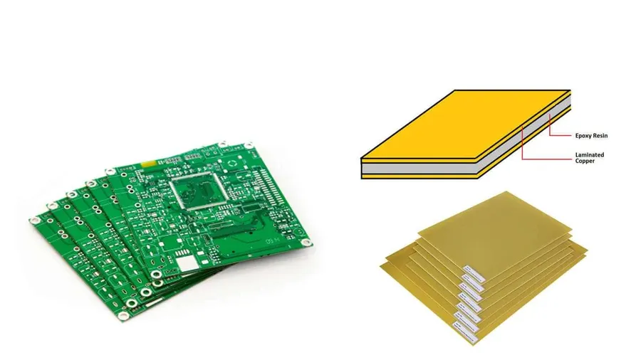
A bare PCB, or Printed Circuit Board, represents the fundamental building block of nearly all electronic devices. It is a substrate, typically composed of fiberglass or composite materials, upon which conductive pathways are etched, forming the intricate network of circuits. Crucially, a bare PCB is devoid of any electronic components; it is the 'blank canvas' awaiting population with resistors, capacitors, integrated circuits, and other active and passive elements.
Bare PCB Manufacturing Process
The manufacturing of bare PCBs is a complex, multi-stage process requiring high precision and careful control at each step to ensure the final product meets stringent quality standards. This process transforms raw materials into the foundational circuit boards upon which electronic components are assembled.
The process generally includes these key stages:
- Design and Layout
The process begins with the electronic circuit design, typically created using specialized software. This design dictates the precise arrangement of conductive traces, pads, and vias on the PCB. Gerber files, an industry-standard format, are generated from the design and used to control manufacturing equipment. - Material Selection
The choice of substrate material, most commonly FR-4 (a glass-reinforced epoxy laminate), is critical. Other materials such as polyimide (for flexible PCBs) or metal cores may be selected based on application-specific requirements, such as thermal performance or flexibility. - Inner Layer Imaging
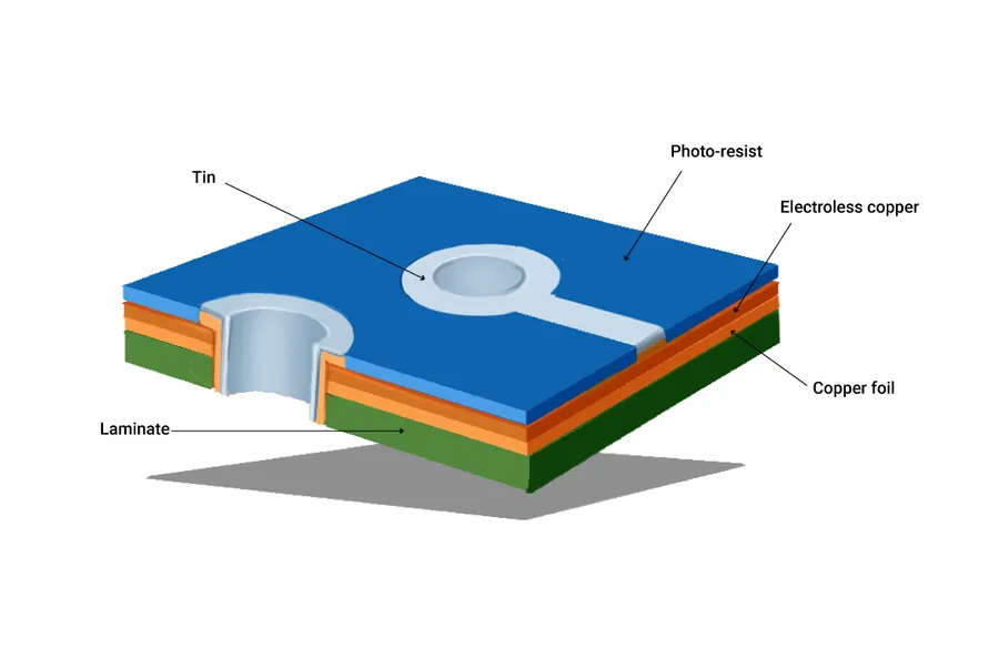
For multilayer boards, this step is critical for each layer. A photosensitive film is applied to a copper clad laminate, exposed to UV light through a film mask which contains the circuit pattern of the inner layer, and then developed to reveal the pattern. This process transfers the desired circuit pattern to the copper layer. - Etching
The copper laminate is treated to remove the unwanted copper areas, leaving behind the designed circuit pattern. This process typically involves using chemical etchants which react with and dissolve the copper not protected by the developed photoresist. - Lamination
Multiple etched layers, along with prepreg layers (insulating layers of partially cured resin), are stacked and laminated under heat and pressure. This process bonds the layers together to create a multi-layer PCB. Precise alignment is crucial during this step to ensure the layers connect as designed. - Drilling
Holes for component leads and vias (interlayer connections) are precisely drilled using CNC machines. These drills range in diameter based on the design requirements, with tight tolerances to ensure proper connectivity and alignment. - Plating
The drilled holes are chemically plated with copper to form conductive vias for interlayer connections. This is achieved through electrochemical deposition in a specialized plating bath. This process allows for electrical connectivity between PCB layers. The surface copper is also often plated to improve solderability. - Outer Layer Imaging
Similar to the inner layer process, the outer copper layers receive photoresist and are patterned using UV exposure and developing. - Final Etching and Plating
The outer layers of copper are etched and then plated with a protective coating, typically solder mask and a finish, which is often immersion gold or tin. This protects the exposed copper from oxidation and also provides a solderable surface for component attachment. - Solder Mask Application
A solder mask, which is a protective coating, is applied to the PCB except on the solder pads to prevent solder bridges during the component assembly process. This mask protects conductive paths from shorts and other assembly defects. - Silkscreen Printing
A silkscreen layer which provides visual identification for components, test points, and the manufacturer's name is applied using an ink printing process. This layer provides information for component assembly and testing. - Final Inspection and Testing
The final bare boards are visually inspected, and electrically tested for shorts and opens to confirm the board is manufactured according to design specifications before shipping. This ensures a high level of quality and prevents assembly defects in downstream processes.
Types of Bare PCBs
Bare PCBs are categorized based on several key factors, primarily the materials used in their construction, the number of conductive layers they incorporate, and their intended applications. These classifications impact performance, cost, and suitability for different electronic devices.
| Category | Description | Typical Applications | Advantages | Disadvantages |
|---|---|---|---|---|
| Based on Material | FR-4 (Flame Retardant 4): Most common material, a fiberglass epoxy laminate. Flex PCBs: Made from flexible substrates like polyimide or polyester. | FR-4: General-purpose electronics. Flex: Wearable devices, automotive, aerospace. | FR-4: Cost-effective, good mechanical and electrical properties. Flex: Lightweight, flexible, high-density packaging. | FR-4: Rigid. Flex: More expensive, temperature-sensitive. |
| Based on Layers | Single-Layer: One conductive layer. Double-Layer: Two conductive layers on opposite sides. Multi-Layer: Three or more conductive layers. | Single-Layer: Simple circuits. Double-Layer: Moderate complexity. Multi-Layer: High-density, complex electronics. | Single-Layer: Lowest cost, simplest designs. Double-Layer: More complex routing. Multi-Layer: Highest density, complex interconnects. | Single-Layer: Limited routing complexity. Double-Layer: Larger size, more complex routing. Multi-Layer: Most expensive, more complex design. |
| Based on Application | Rigid PCBs: Traditional PCBs, rigid and inflexible. Flexible PCBs: Bendable and conformable. Rigid-Flex PCBs: Combination of both rigid and flexible regions. | Rigid: Most applications. Flex: Wearables, curved surfaces. Rigid-Flex: Complex systems with space constraints. | Rigid: Most common, economical. Flex: High flexibility, space savings. Rigid-Flex: Versatile design, compact form factor. | Rigid: Inflexible. Flex: Higher cost, challenging to assemble. Rigid-Flex: Complex design and manufacturing, higher cost. |
Importance of Bare PCB Testing
Bare PCB testing is a crucial step in the manufacturing process, ensuring the integrity of the circuit board before costly electronic components are assembled. Detecting defects at this stage significantly reduces overall manufacturing costs and prevents potential failures in the final product. The primary goal of bare PCB testing is to identify any shorts, opens, or other manufacturing flaws that could compromise the functionality of the assembled board.
Two primary testing methods are employed: electrical testing and visual inspection. These methods are complementary, providing comprehensive coverage of potential defects.
Bare PCB Applications
Bare PCBs serve as the foundational building blocks for a vast array of electronic devices across numerous industries. Their versatility stems from the ability to be customized and populated with specific electronic components, making them indispensable in modern technology. The following sections will highlight some key sectors where bare PCBs are integral.
- Consumer Electronics
Bare PCBs are the foundation for devices such as smartphones, laptops, tablets, digital cameras, and televisions. Their ability to be made small and to high-density requirements are key for these devices. - Automotive Industry
From engine control units (ECUs) and advanced driver-assistance systems (ADAS) to in-car entertainment systems and safety features, bare PCBs enable the complex electronics in modern vehicles. These PCBs must withstand harsh conditions like vibration and extreme temperatures. - Aerospace and Defense
In aviation, bare PCBs are crucial components for avionics, navigation systems, radar, communication devices, and control systems where reliability is paramount. They are also vital in defense applications including communication equipment and weapon systems. - Medical Devices
Bare PCBs are critical in medical imaging equipment such as MRI, CT scanners, patient monitoring systems, and surgical instruments. The stringent requirements of medical applications demand high levels of quality and precision. - Industrial Automation
Bare PCBs underpin various industrial automation systems including programmable logic controllers (PLCs), robotics, and control equipment. These PCBs need to be robust to operate in a variety of industrial environments. - Telecommunications
In the telecommunications sector, bare PCBs are used in base stations, networking equipment, routers, switches and mobile communication devices, enabling seamless communication networks. - Renewable Energy
Bare PCBs are found in solar inverters, wind turbine control systems, and smart grid technologies, contributing to the growth of renewable energy sectors.
Advantages of Using Bare PCBs
Utilizing bare PCBs offers significant advantages in electronic product development, impacting performance, reliability, and cost-effectiveness. The inherent control over the board's quality at this stage is paramount, as any defects here will propagate through the assembly process and compromise the end product.
- Enhanced Product Performance
High-quality bare PCBs ensure optimal signal integrity and minimize signal loss. Precise trace widths, controlled impedance, and proper layer stack-up result in more efficient power distribution, leading to improved performance of the final electronic device. Furthermore, selecting appropriate materials with specific dielectric properties and thermal coefficients of expansion are vital for performance optimization. - Superior Reliability
By testing bare PCBs thoroughly, potential issues such as short circuits, open circuits, and plating defects are identified and rectified before any costly components are mounted. This proactive approach prevents failures in the field and leads to a more reliable end product, increasing its lifespan and reducing the risks of early component failure. For instance, a reliable solder mask application enhances durability and reduces corrosion risks in humid operating environments. - Cost-Effectiveness
Detecting and correcting defects at the bare PCB stage is significantly less expensive than troubleshooting issues after components are assembled. Rework on a populated PCB is costly and time-consuming. By rigorously testing at this initial stage, manufacturers minimize material waste, reduce repair costs, and streamline the entire production cycle, achieving substantial cost savings in the long run. Early detection of defects also minimizes the need for more sophisticated (and expensive) testing later. - Design Flexibility and Customization
Bare PCBs offer maximum design flexibility, allowing for precise customization tailored to specific application requirements. This includes controlling the number of layers, materials, and trace widths, enabling engineers to meet diverse performance requirements. It also facilitates easy integration with other board components in later assembly processes. - Improved Assembly Efficiency
Consistent and high-quality bare PCBs simplify the assembly process. The reduction in defects at the bare board level directly translates into a smoother, less problematic component mounting process. This ultimately reduces labor costs and throughput time during the PCBA assembly stage, further contributing to cost-effectiveness.
Key Differences between a Bare PCB and a Populated PCB (PCBA)
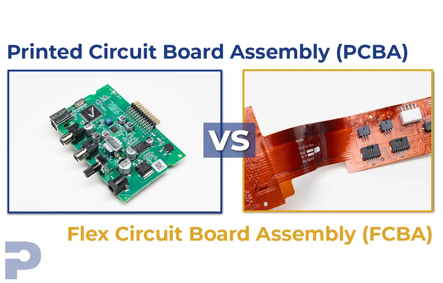
The core distinction between a bare PCB and a populated PCB (PCBA) lies in the presence of electronic components. A bare PCB is the foundational circuit board, consisting of conductive pathways and pads on a substrate, ready to receive components. In contrast, a PCBA is a bare PCB that has undergone a population process, where electronic components like resistors, capacitors, integrated circuits, and connectors are soldered onto the board, forming a complete functional circuit.
| Feature | Bare PCB | Populated PCB (PCBA) |
|---|---|---|
| Components | No electronic components | Electronic components soldered on |
| Functionality | Non-functional as a circuit | Fully functional circuit |
| Appearance | Exposed copper traces and pads | Components mounted on the board |
| Usage | Intermediate product for assembly | Ready to use or part of a device |
| Cost | Lower cost compared to PCBA | Higher cost due to component costs and assembly |
Frequently Asked Questions About Bare PCBs
This section addresses common questions regarding bare PCBs, providing clarity on their characteristics, manufacturing, and applications. We aim to resolve any confusion and provide concise, technically accurate answers based on established engineering principles.
- What exactly is a bare PCB?
A bare PCB, or Printed Circuit Board, is the foundational substrate of electronic devices. It's a board made of insulating material (such as FR-4) with conductive traces (usually copper) etched onto its surface. It acts as a base for mounting and connecting electronic components but contains no components itself. - What is the difference between a bare PCB and a blank PCB?
The terms 'bare PCB' and 'blank PCB' are often used interchangeably and refer to the same thing: a PCB without any electronic components attached. They both represent the starting point before the population process begins. - What is meant by 'bear pcb'?
The term 'bear pcb' is likely a misspelling of 'bare pcb.' Both terms reference the unpopulated PCB. - What are some common defects found in bare PCBs?
Common defects in bare PCBs include shorts (unintended electrical connections), opens (breaks in conductive traces), misaligned layers, insufficient plating, and dimensional inaccuracies. These defects can be caused by issues in the manufacturing process and can lead to significant problems in the final product. Rigorous testing, including electrical and visual inspection, is critical to detect these defects before component assembly. - How does a bare PCB differ from a PCBA (Printed Circuit Board Assembly)?
A bare PCB is simply the board with conductive traces but without any electronic components. A PCBA, or Printed Circuit Board Assembly, on the other hand, includes the bare PCB with all the necessary electronic components (resistors, capacitors, integrated circuits, etc.) soldered onto it. The PCBA is the functional circuit ready to be incorporated into a device. - How do I choose the right bare PCB manufacturer?
Selecting a suitable bare PCB manufacturer requires careful consideration of several factors. These include the manufacturer's experience, production capabilities (e.g., layer count, material options, tolerances), quality control procedures, lead times, and pricing. It's also crucial to review certifications and to seek samples and references to ensure the manufacturer can meet your specific requirements. Additionally, effective communication and customer service are key to a smooth process. - What factors influence the price of a bare PCB?
The price of a bare PCB is determined by several factors, including material type (e.g., FR-4, flex), number of layers, board size, complexity of design (density of traces, via count), surface finish (e.g., ENIG, HASL), order volume, and production lead time. More complex designs with higher layer counts and tighter tolerances typically result in higher costs, as does rush production.
The bare PCB, often unseen yet crucial, forms the backbone of modern electronics. It's the initial canvas where electronic circuits come to life. From the intricate manufacturing processes to rigorous testing and diverse applications, bare PCBs are essential for reliable and functional electronic devices. Understanding the intricacies of bare PCBs highlights the complexity and precision behind the technology that powers our daily lives. As technology continues to advance, the importance of high-quality bare PCBs will only become more crucial in ensuring the performance and reliability of every electronic gadget.