Understanding Patch PCBs: Design, Functionality, and Applications
In our interconnected world, the humble printed circuit board (PCB) plays a pivotal role. One specific type, the patch PCB, is essential in many electronic applications. From communication devices to advanced sensor technologies, patch PCBs are the foundation of wireless connectivity, utilizing their unique structure to create effective antennas. This article dives deep into the design, functionality, and practical applications of patch PCBs, shedding light on their importance in modern technology.
What is a Patch PCB?
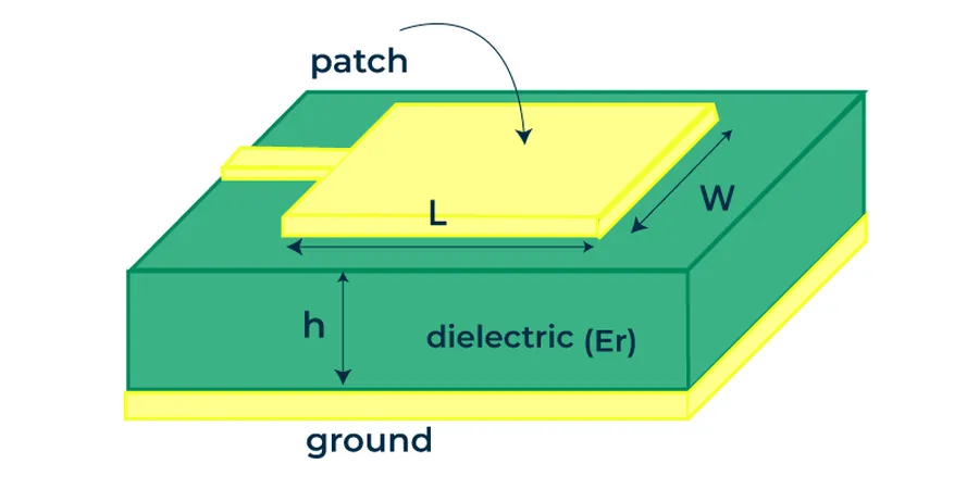
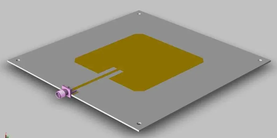
A patch PCB, at its core, is a microstrip antenna fabricated directly onto a printed circuit board (PCB). This type of antenna is characterized by a conductive 'patch' of metal, typically copper, separated from a ground plane by a dielectric substrate. Unlike traditional antennas, which are often discrete components, patch antennas are integrated directly into the PCB structure, making them a compact and cost-effective solution for wireless communication.
The key components of a patch PCB antenna are the radiating patch, the dielectric substrate, and the ground plane. The shape and size of the patch, the properties of the dielectric, and the distance between the patch and the ground plane are crucial factors that determine the antenna's performance characteristics, including its resonant frequency, bandwidth, and radiation pattern. The functionality of a patch PCB relies on the principles of electromagnetic radiation, where the oscillating electric field within the patch creates a propagating electromagnetic wave.
How Patch PCBs Function as Antennas
Patch PCBs operate as antennas by radiating electromagnetic energy, functioning as a resonant structure that efficiently converts electrical signals into radio waves. This functionality hinges on the precise geometry of the conductive patch and the substrate material, coupled with the principles of electromagnetic field theory, specifically regarding how radio waves are generated and propagated.
At the heart of a patch PCB antenna's operation are several key elements. The conductive patch, typically a rectangle or a circle, serves as the primary radiating element. This patch is positioned over a dielectric substrate, which provides mechanical support and also influences the antenna's electromagnetic properties. Crucially, there is a ground plane located on the opposite side of the substrate, which acts as a reflector and is essential for establishing the desired radiation pattern. Radio frequency signals are fed to the patch, initiating oscillations of current that ultimately generate electromagnetic waves.
The physics of radio wave transmission are fundamental to the function of patch PCBs. When an alternating current is applied to the patch, it creates an oscillating electromagnetic field around it. This field causes radio waves to radiate outward, with the ground plane guiding the radiation. The size and shape of the patch are engineered such that it resonates at a specific frequency, efficiently radiating energy at this frequency. Efficient signal radiation is critically dependent on achieving proper impedance matching, and can be achieved using different techniques, including tuning stubs and quarter wave transformers.
Radiation patterns define how the antenna radiates power in different directions and affect signal coverage and quality. These patterns are determined by the geometry of the patch and its position in relation to the ground plane. For instance, a rectangular patch antenna may have a broad radiation pattern while a more complex shape, like a circular patch, may provide a more directional pattern. Proper antenna design ensures that the radiated energy is focused in the desired direction, maximizing signal strength for the intended application.
The shape and size of the patch directly impact the antenna's resonant frequency, bandwidth, and radiation pattern. Generally, a larger patch will resonate at a lower frequency while its shape affects the way the electromagnetic fields are distributed, which defines its directional properties. Therefore, precise tuning of these factors is crucial in optimizing antenna performance for specific applications and ensuring the design meets the requirements, including range and data transfer rate.
Types of Patch PCB Antennas

Patch PCB antennas come in various shapes, each offering unique performance characteristics suitable for different applications. The geometry of the radiating element significantly influences the antenna's resonant frequency, bandwidth, and radiation pattern. Understanding these differences is crucial for selecting the optimal antenna for a specific design.
| Antenna Type | Description | Advantages | Disadvantages | Typical Applications |
|---|---|---|---|---|
| Rectangular Patch | The most common type, characterized by a rectangular radiating element. | Simple design, easy to analyze and fabricate, good for general applications. | Can be relatively narrow bandwidth compared to other types, lower gain than others. | Wi-Fi, Bluetooth, general communication systems. |
| Circular Patch | Features a circular radiating element. | Good polarization purity, can be designed for wide bandwidths, and easier to achieve circular polarization. | More complex analysis and design than rectangular patches, can be larger for the same operating frequency. | GPS, satellite communication, RFID. |
| Square Patch | A special case of the rectangular patch where the length and width are equal. | Balanced performance, slightly wider bandwidth compared to a standard rectangular patch, good compromise between complexity and functionality. | Can still have limited bandwidth, especially at higher frequencies. | Wi-Fi, Bluetooth, general communication systems. |
| Triangular Patch | Radiating element is shaped like a triangle, most often equilateral or right-angled triangles. | More compact than other designs, can achieve wideband characteristics. | More complex design and analysis than rectangular or square patches. | Mobile devices, compact communication devices. |
| Elliptical Patch | Radiating element has an elliptical shape. | Enhanced flexibility for adjusting impedance and bandwidth, can achieve circular polarization | More complex manufacturing, analysis is complex. | Specialized applications such as satellite communication. |
| Slot Antennas | Formed by a slot or opening in the PCB's ground plane. | Easy integration into multilayer PCBs, relatively low profile, broad bandwidths possible. | Can be more sensitive to manufacturing tolerances, require careful design to avoid unwanted radiation. | Applications where space is restricted, such as mobile and wearable devices. |
The selection of a specific patch antenna type depends on the desired performance characteristics and the constraints of the application. Key factors include operating frequency, bandwidth requirements, polarization needs, gain, size restrictions, and fabrication complexities. Careful analysis and simulations are essential to optimize the design for efficient operation.
Design Considerations for Patch PCBs
Designing patch PCBs requires careful consideration of several critical factors to achieve the desired antenna performance. This includes substrate selection, material properties, and manufacturing tolerances, which all significantly affect the antenna’s resonant frequency, bandwidth, and radiation pattern.
Key design considerations are:
- Substrate Selection
The substrate material's dielectric constant (εr) and loss tangent (tan δ) significantly impact the antenna's performance. Materials like FR-4 are cost-effective but may have higher losses at higher frequencies. High-frequency substrates such as Rogers or PTFE offer lower losses and more stable performance but at a higher cost. - Material Properties
The thickness of the substrate and copper cladding are crucial parameters for controlling the antenna's impedance and bandwidth. Variations in these parameters can lead to deviations in performance. Proper understanding of material properties in relation to temperature and humidity is critical for performance over a wide range of operational conditions. - Manufacturing Tolerances
Precise manufacturing is essential for achieving the desired resonant frequency and impedance matching. Variations in etching processes and trace dimensions can result in performance deviations. Controlled etching processes and precise component placement are crucial to maintain antenna performance within designed specifications. - Frequency of Operation
The frequency determines the physical dimensions of the patch antenna. Higher frequency operation results in smaller antenna sizes. The antenna's dimensions must be accurately calculated using formulas specific to the patch shape, which relates the physical parameters of the antenna to its resonant frequency. - Bandwidth Requirements
Patch antennas inherently have narrow bandwidths, so design techniques like impedance matching and the use of specific shapes must be employed to increase the usable frequency range. Different feeding techniques can affect bandwidth as well. - Radiation Pattern
The radiation pattern of the patch antenna is affected by its shape, size, and feeding method. A directional pattern may be needed for point-to-point communication, while an omnidirectional pattern may be required for broad area coverage. The radiation pattern needs to be simulated and optimized to achieve desired coverage areas and reduced interference.
| Design Parameter | Impact | Considerations |
|---|---|---|
| Substrate Dielectric Constant (εr) | Affects antenna size and resonant frequency | Choose a material that meets the size and frequency requirements for the application |
| Substrate Loss Tangent (tan δ) | Impacts efficiency | Use material with low loss tangent, especially at high frequencies |
| Substrate Thickness | Influences bandwidth and impedance | Optimize thickness for bandwidth and efficient coupling |
| Copper Trace Dimensions | Determines antenna impedance and radiation pattern | Fabricate copper layer with tight tolerances |
| Antenna Shape | Directly affects radiation pattern and bandwidth | Select the suitable antenna shape based on the radiation and bandwith specifications |
| Feed Line Position | Crucial for impedance matching | Optimize the location of the feed line to ensure optimum impedance |
Integrating Patch PCBs into Larger Systems
Successfully integrating patch PCBs into larger electronic systems requires careful consideration of several crucial factors to ensure optimal performance and reliability. These factors extend beyond the antenna design itself, encompassing thermal management, electromagnetic interference (EMI) protection, and strategic physical placement within the overall system architecture.
- Thermal Management
Patch PCBs can generate heat, especially when handling high power signals. Adequate thermal management is crucial to maintain performance and prevent damage. Strategies include heat sinks, thermal vias, and careful material selection to ensure proper heat dissipation from the PCB. - EMI Protection
Patch PCBs can be susceptible to or cause electromagnetic interference. To minimize EMI, the integration should incorporate shielding, grounding techniques, and proper placement of components to prevent unwanted signal coupling and maintain signal integrity. Consider using grounded enclosures or Faraday cages to shield sensitive components. - Physical Placement
The physical location of the patch PCB within the larger system can significantly affect its performance. Avoid placing the antenna near metallic objects or other components that can cause signal reflection, absorption, or detuning. Optimal placement typically involves maximizing the clear space around the antenna element to ensure a clean radiation pattern. - Impedance Matching and System Integration
Achieving optimal performance requires careful impedance matching between the patch PCB and the other components in the system, such as RF transceivers or amplifiers. Inappropriate impedance matching can lead to significant signal loss and reduced performance, so designing an effective impedance matching network is critical. - Mechanical Considerations
The mechanical design of the system must accommodate the patch PCB without applying stress or pressure that could alter its performance characteristics. Ensure adequate support and consider the mechanical tolerances of the system and the PCB, as well as any potential vibration or shock that could affect performance. - Testing and Validation
Thorough testing and validation are critical after integration. This includes testing the antenna's radiation pattern, impedance, and overall system performance to ensure the integrated system operates as expected under real-world conditions. Use calibrated RF equipment to ensure measurement accuracy.
Patch PCB Applications
Patch PCBs, owing to their low profile, ease of manufacturing, and cost-effectiveness, find extensive applications across diverse sectors. They are integral in devices requiring wireless communication, location tracking, and identification. This section will detail some key applications where patch PCBs play a crucial role.
- WiFi Routers
Patch PCBs are commonly used as embedded antennas in WiFi routers and access points. Their ability to be directly integrated onto the main PCB reduces cost and complexity. They facilitate wireless connectivity for internet access across homes, offices, and public spaces. The performance and reliability of the WiFi signal depends on careful design of the patch antenna. - GPS Devices
In GPS devices, patch PCBs serve as antennas for receiving signals from GPS satellites. These are crucial components enabling accurate location tracking for navigation systems, handheld GPS devices, and asset tracking applications. The design of the patch needs to ensure reception of weak signals in a wide bandwidth. - RFID Systems
Patch PCB antennas are utilized in RFID (Radio-Frequency Identification) systems for tracking and identifying items. These systems can be found in various sectors such as retail, logistics, and healthcare. Patch antennas are suitable for close proximity communication, making them effective for item tagging, access control, and inventory management, and typically operate in the UHF band. - Medical Implants
In medical implants, patch antennas on a PCB enable wireless communication for monitoring physiological data, drug delivery, or nerve stimulation. These implants necessitate a low-profile, biocompatible, and highly efficient antenna designs to ensure reliable wireless communication within the human body. Compliance with strict medical regulations on material safety and radiation is paramount. - IoT Devices
The Internet of Things (IoT) is experiencing a surge, with patch PCBs being fundamental for providing wireless connectivity to a wide array of devices. From smart home sensors to industrial monitoring systems, patch antennas provide low cost, ease of manufacture and robust communication in compact sizes. The efficiency of power consumption and design compatibility are crucial in IoT device integration. - 5G Technology
5G technology, with its higher frequency bands, needs sophisticated antennas. Patch PCBs can be manufactured to support 5G applications, including beamforming for directed signal transmission. They are becoming important for both infrastructure and mobile devices, and can be designed to work in the mmWave bands with high precision manufacturing techniques.
Advantages and Limitations of Patch PCBs
Patch PCBs offer a compelling blend of advantages and limitations, making them suitable for a range of applications while also presenting certain challenges. Understanding these trade-offs is crucial for effective design and deployment.
| Feature | Advantages | Limitations | Mitigation Strategies |
|---|---|---|---|
| Profile | Low profile, allowing for compact and integrated designs. | May be too fragile for some applications with high mechanical stress. | Implement protective housing or encapsulation for sensitive applications. |
| Cost | Cost-effective to manufacture, especially in high volumes. | Initial design and prototyping can incur costs. | Leverage design reuse and simulation tools. |
| Manufacturing | Easy to fabricate using standard PCB manufacturing processes. | Manufacturing tolerances can impact antenna performance. | Use high precision fabrication techniques. |
| Bandwidth | Relatively narrow bandwidth compared to other antennas. | Restricts applications to specific frequency bands. | Use techniques such as impedance matching, tuning circuits, and stacked patch designs to achieve wider bandwidth. |
| Gain | Moderate gain, suitable for short to medium range communications. | Not ideal for long distance communications. | Use higher gain antenna elements or arrays of patch antennas. |
| Polarization | Offers options for linear or circular polarization. | Cross-polarization sensitivity can cause signal loss if not accounted for. | Carefully align transmitting and receiving antennas. |
| Environmental | Good performance in controlled environments. | Performance can be affected by temperature and humidity fluctuations. | Choose substrate materials with low temperature coefficient and implement temperature compensation circuitry when needed. |
Frequently Asked Questions About Patch PCBs
This section addresses common queries regarding patch PCBs, providing concise and authoritative answers to enhance understanding and practical application.
- What are the common methods for matching impedance in patch PCBs?
Impedance matching in patch PCBs is crucial for efficient power transfer and minimizing signal reflections. Common methods include using quarter-wave transformers, inset feeds, and reactive impedance matching networks. Quarter-wave transformers employ a section of transmission line with a specific impedance and length (typically one-quarter of the operating wavelength) to transform the impedance. Inset feeds adjust the feed position relative to the patch to manipulate the input impedance. Reactive impedance matching networks use lumped elements like capacitors and inductors to achieve the desired impedance. Each of these methods is selected based on the desired bandwidth, performance, and the complexity of the design. - Can patch PCBs be used for ultra-wideband applications?
While patch antennas are inherently narrowband due to their resonant nature, techniques exist to broaden their bandwidth, enabling them for use in ultra-wideband (UWB) applications. These techniques include using impedance matching circuits with multiple resonators, employing stacked patch designs, or implementing parasitic elements. However, the performance of patch antennas for UWB is usually a tradeoff between bandwidth and overall gain. Special designs and impedance matching circuits are required to handle wide range of frequencies, which also leads to more complex design and manufacturering. - How to troubleshoot issues with patch PCBs not working correctly?
Troubleshooting patch PCBs involves systematic checks across design, fabrication and application of the antenna. Firstly, confirm the designed dimensions against the manufactured board. A crucial step is verifying impedance matching of the antenna using a Vector Network Analyzer (VNA). Another area to look at is the substrate material and its dielectric properties, which can vary from design specifications. Also verify the signal feed path and solder joints for continuity and proper connection. Finally, environment conditions around the patch can affect its performance. If none of these steps resolve the issue, the design must be evaluated for correctness or to confirm the antenna was applied in the range of its performance. - What are the common materials for making patch antennas?
Common substrate materials for patch antennas include FR-4 (Flame Retardant 4), Rogers materials (e.g., Rogers 4350, Rogers 5880), and ceramic substrates. FR-4 is cost-effective and suitable for many applications, but it has higher dielectric losses at higher frequencies. Rogers materials offer lower dielectric losses, making them ideal for high-frequency or higher power applications where efficiency is essential. Ceramic substrates have high dielectric constants, which help to reduce the size of antennas. The choice of material depends on the operating frequency, performance requirements, and cost considerations. - What are the differences between patch antennas and other types of antennas?
Patch antennas, also known as microstrip antennas, are characterized by their planar structure, low profile, and ease of fabrication on printed circuit boards. Compared to other types of antennas, like dipoles or horn antennas, patch antennas are more compact and less obtrusive. Dipoles are relatively simple but are not planar, while horn antennas have higher gain but are bulky. Patch antennas offer a good balance between size, performance, and ease of integration, making them suitable for many wireless applications. Their bandwidth, though, is usually lower than other options. - Is it possible to design a patch PCB antenna with impedance matching?
Yes, it is absolutely possible, and indeed essential, to design a patch PCB antenna with impedance matching to maximize the power transfer and reduce reflections. Proper impedance matching ensures that the antenna efficiently radiates the signal provided to it. Techniques like inset feed, microstrip matching networks, and quarter-wave transformers can be integrated directly into the PCB layout. Careful selection of the feed point and precise dimensions are critical for impedance matching to the source signal and the system to which it is connected. - What are the trade-offs when using different substrates for patch antennas?
The choice of substrate material for a patch antenna involves trade-offs. FR-4 is cheap and easy to fabricate, but its high dielectric loss is a drawback at higher frequencies. Higher quality substrates such as Rogers materials, offer much better loss characteristics which is critical for high frequency applications, but they come at a higher cost. Ceramic substrates can shrink the antenna dimensions due to higher dielectric constants, but they are more brittle and can be costly to process. The selection usually involves trade-offs between cost, performance, frequency, power handling and overall system requirements.
Future Trends and Innovations in Patch PCB Technology
The field of patch PCB technology is rapidly evolving, driven by the increasing demands for higher performance, smaller size, and greater versatility in wireless communication systems. Emerging trends focus on advanced materials, innovative designs, and integration strategies to overcome the traditional limitations of patch antennas.
- Metamaterial Antennas
Metamaterials are engineered materials with properties not found in nature. Integrating these materials into patch PCB designs allows for unprecedented control over electromagnetic waves, enabling the creation of antennas with enhanced directivity, bandwidth, and efficiency. Metamaterial-based patch antennas can achieve unique radiation patterns and miniaturization, making them suitable for advanced applications. - Tunable Patch Antennas
Tunable antennas offer the capability to adjust their operating frequency in real-time. This is achieved by integrating active components such as varactor diodes or MEMS switches directly onto the patch PCB. Tunable patch antennas are crucial for applications requiring adaptive bandwidth or frequency hopping, providing greater flexibility and performance in dynamic environments. - Multi-Layer Patch PCB Designs
Multi-layer PCB technology is being utilized to improve the performance of patch antennas. By stacking multiple patch elements and dielectric layers, designers can achieve wider bandwidth, higher gain, and more complex radiation patterns. Multi-layer designs also facilitate the integration of matching networks and other components directly within the antenna structure, reducing size and enhancing overall system performance. - Integration with Advanced Materials
Research into advanced substrate materials with lower dielectric constants and losses is critical. Materials such as liquid crystal polymers (LCP) and ceramics are being explored to reduce the size and improve the efficiency of patch PCB antennas. These advanced materials enable higher performance at higher frequencies. - AI-Driven Design Optimization
Artificial intelligence (AI) and machine learning (ML) are increasingly being used to optimize patch antenna designs. AI algorithms can rapidly explore vast design spaces, identify optimal parameters, and predict antenna performance with high accuracy, accelerating the design process and improving outcomes.
Patch PCBs represent a significant advancement in antenna technology, providing a versatile, compact, and cost-effective solution for a multitude of applications. From understanding their design principles to implementing them in complex systems, this article has provided a foundational knowledge base. As we move further into a wireless future, the importance of patch PCBs will only continue to grow, necessitating further innovations and optimized solutions for diverse electronic needs and applications. By understanding the nuances of patch PCB technology, developers and engineers can harness their full potential, ensuring the next generation of electronic devices are both functional and efficient.