Understanding PCB Electronics: A Comprehensive Guide
In today's tech-driven world, the printed circuit board, or PCB, is the unsung hero of almost every electronic device we use. From smartphones to satellites, PCBs provide the essential platform for connecting electronic components. Understanding PCB electronics is crucial for anyone looking to delve deeper into the mechanics of technology, making the invisible infrastructure of our gadgets visible and understandable. This article provides a comprehensive overview of PCB electronics, explaining their function, design, various types, and their impact on our daily lives.
What is a Printed Circuit Board (PCB)?
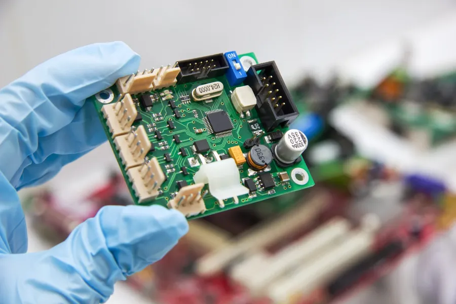
A Printed Circuit Board (PCB) is the foundational platform upon which electronic components are mounted and interconnected to form a functional electronic circuit. PCBs utilize a non-conductive substrate, typically composed of materials like fiberglass or epoxy, onto which conductive pathways, known as traces, are etched, typically from copper. These traces, along with other features like pads and vias, create the necessary electrical connections between components, thereby enabling the flow of electrical current and facilitating the desired electronic functionality.
The PCB's core function lies in providing both structural support and electrical connectivity for electronic components. The process of constructing a PCB involves a meticulous sequence of steps, including design, etching, and assembly, resulting in a critical component that underpins the vast majority of electronic devices today. Without PCBs, the reliable and compact integration of electronic circuits would be fundamentally unachievable.
The Fundamental Role of PCBs in Electronics
Printed circuit boards (PCBs) are indispensable components in the modern electronics industry, serving as the bedrock upon which nearly all electronic devices are built. Their primary function extends beyond simple structural support; they provide a stable and reliable platform for mounting electronic components, establishing precise electrical connections, and facilitating the creation of complex and intricate circuits. PCBs are fundamental to the operation and functionality of today's advanced electronics.
The use of PCBs has revolutionized electronics by moving away from cumbersome point-to-point wiring, thereby significantly increasing the reliability, miniaturization, and mass producibility of electronic devices. Without PCBs, many of the technological advances of the past few decades would be unachievable.
- Platform for Component Mounting
PCBs offer a robust and consistent foundation for the secure placement of electronic components, ensuring that they remain stable and do not shift during operation. - Efficient Electrical Connections
They establish precise electrical pathways, which are crucial for maintaining signal integrity, minimizing interference, and ensuring optimal circuit performance. - Support for Complex Circuitry
PCBs allow for the creation of intricate and multi-layered circuits, enabling the design of increasingly complex electronic devices, ranging from simple controllers to sophisticated processors. - Enhanced Reliability and Durability
By providing a structured environment for connections, PCBs improve the mechanical stability and resistance to physical damage of the entire circuit. - Facilitate Mass Production
The PCB manufacturing process enables mass production with high repeatability and efficiency, reducing manufacturing costs and enhancing the availability of electronic products.
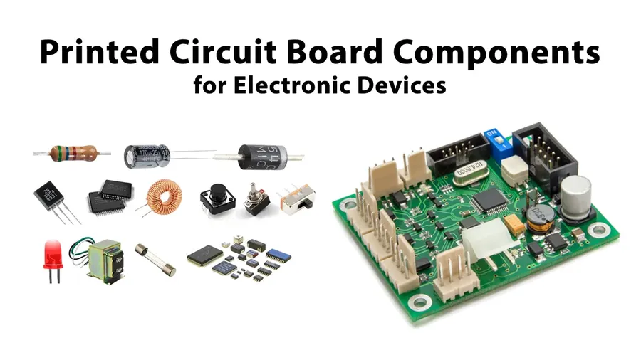
Key Components of a PCB
A Printed Circuit Board (PCB) is a complex assembly composed of several key elements that work together to facilitate the creation of electronic circuits. These components, including substrate materials, copper layers, vias, pads, solder mask, and silkscreen, are fundamental to the functionality and reliability of the PCB and its application in electronic devices. Each element has a specific role to play in ensuring proper electrical connections and mechanical stability.
| Component | Description | Function | Materials |
|---|---|---|---|
| Substrate | The base material of the PCB. | Provides mechanical support and insulation for other components. | Typically FR-4 (fiberglass-reinforced epoxy), but can include other materials like polyimide or aluminum. |
| Copper Layers | Thin layers of copper foil that are etched to form conductive traces. | Provide the conductive pathways for electrical signals and power. | Copper, typically with a thickness measured in ounces per square foot (oz/ft²). |
| Vias | Plated through-holes that connect conductive layers. | Enable electrical connections between different layers of the PCB. | Copper plating inside a drilled hole, usually with a protective plating. |
| Pads | Small areas of copper on the surface of the PCB. | Provide connection points for soldering electronic components. | Copper, typically with a surface finish like HASL (Hot Air Solder Leveling) or ENIG (Electroless Nickel Immersion Gold). |
| Solder Mask | A protective layer applied to the PCB surface. | Prevents solder bridging and protects conductive traces from corrosion. | Epoxy-based polymer material. |
| Silkscreen | A layer of ink printed onto the PCB surface. | Provides component identification, polarity markings, and test points for reference. | Epoxy or acrylic ink. |
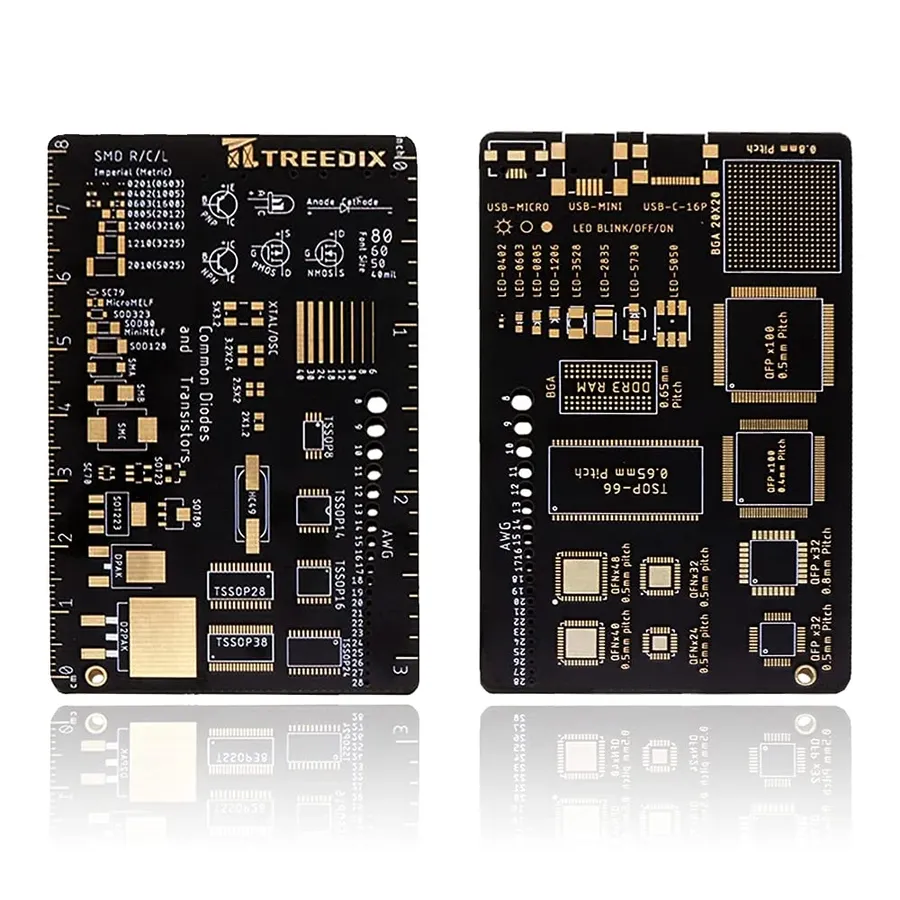
Types of PCBs: Exploring Different Designs
Printed Circuit Boards (PCBs) are not monolithic; they come in a variety of designs, each tailored to specific applications and complexity requirements. Understanding these different types is crucial for selecting the appropriate board for any given electronic project. This section will explore the key differences between single-layer, double-layer, multi-layer, flex, rigid, and rigid-flex PCBs.
| PCB Type | Description | Typical Applications | Advantages | Disadvantages |
|---|---|---|---|---|
| Single-Layer PCB | Features conductive material on one side of the substrate. | Simple electronic circuits, basic appliances, LED lighting. | Low cost, simple design, easy to manufacture. | Limited circuit complexity, difficult to miniaturize. |
| Double-Layer PCB | Has conductive material on both sides of the substrate. | Power supplies, basic control circuits, simple industrial control boards. | Increased circuit density compared to single-layer, more design flexibility. | More complex than single-layer, more expensive. |
| Multi-Layer PCB | Consists of three or more layers of conductive material, separated by insulating layers. | Complex electronics such as smartphones, computers, high-speed communication devices. | High circuit density, high performance, miniaturization possible. | High cost, complex manufacturing process. |
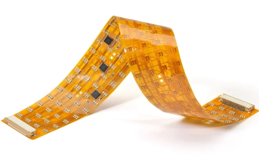
| Flex PCB | Made from flexible substrates like polyimide, allowing the board to bend and flex. | Wearable electronics, flexible displays, automotive electronics. | Flexibility, lightweight, high reliability in dynamic applications. | Higher cost compared to rigid PCBs, requires specialized manufacturing processes. |
| Rigid PCB | Made from a solid substrate that does not bend or flex, such as FR-4. | Most common electronic devices, consumer electronics, industrial equipment. | Cost effective, durable, readily available. | Not suitable for applications requiring flexibility. |
| Rigid-Flex PCB | Combines rigid and flexible sections on the same board. | Aerospace, medical devices, high-end industrial equipment. | Combines advantages of both rigid and flex PCBs, design flexibility. | Complex manufacturing, high cost. |
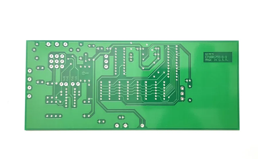
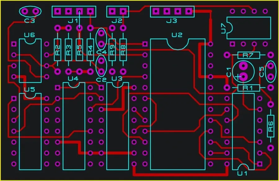
The PCB Manufacturing Process: From Design to Board

The fabrication of a Printed Circuit Board (PCB) is a multi-stage process transforming a digital design into a physical, functional component. This involves a series of precise steps, each crucial to the final performance and reliability of the PCB. From the initial design phase to the final board assembly, meticulous attention to detail is required.
- PCB Design and Layout
The manufacturing process begins with the design of the PCB using CAD software. This includes creating a schematic diagram, which defines the electrical connections, and a layout that specifies the physical locations of the components and traces. The layout is then exported as Gerber files, which are used by PCB manufacturers to fabricate the board. - Film Printing
The Gerber files are used to print the PCB design onto a photographic film. This film is used as a mask during the fabrication process. Accurate printing is critical for the fidelity of the circuit patterns. - Material Preparation
The process starts with the selection of substrate materials, typically FR-4, a glass-reinforced epoxy laminate. The chosen material is then cut to the required panel size. - Copper Cladding
The substrate is coated with a thin layer of copper foil, which serves as the conductive layer. This copper layer is bonded to both sides of the substrate for a double sided PCB, or on a single side for single sided boards, or in various combinations in multi-layer boards. - Etching
The copper is etched away to reveal the desired circuit pattern. The board is first coated with a photoresist, which is then exposed to UV light through the printed film. The exposed photoresist hardens and the unexposed is washed away. The exposed copper is then etched away in a chemical bath, leaving the desired circuit traces. - Drilling
After etching, holes are drilled for component leads and vias (connections between layers). These holes are typically drilled with a computer-controlled drill with high accuracy. - Plating
The drilled holes are then plated with copper to ensure electrical conductivity through the layers. This process creates a conductive pathway in the hole, enabling connections between different layers of the PCB. - Solder Mask Application
A solder mask is applied to the PCB to protect the copper traces from oxidation and to prevent solder bridges during component assembly. The solder mask is a colored polymer coating applied to the entire PCB except the pads which will receive the solder. - Silkscreen Printing
The final step is to apply a silkscreen layer, which consists of labels and markings to help with component placement during assembly, along with other information about the board. - Testing and Quality Control
The finished PCBs are tested for electrical functionality and quality. This includes continuity tests and verification against the original design. Boards that pass quality control are then ready for component assembly. - Component Assembly
Components are placed and soldered onto the board. This process can be automated or manual, depending on the complexity and volume of production. Soldering can be achieved using a variety of methods such as reflow soldering or wave soldering.
Understanding PCB Design Basics
Effective PCB design is crucial for the reliable operation of electronic devices. It involves a systematic approach that begins with schematic capture, progresses to layout design, and takes into account various factors to ensure signal integrity, thermal management, and efficient manufacturing. A well-designed PCB minimizes signal distortion, prevents thermal issues, and facilitates easy component placement and soldering, ultimately resulting in higher-performing and more dependable electronic products.
- Schematic Capture
This initial step involves creating a circuit diagram using electronic design automation (EDA) software. It defines the electrical connections between components and is the blueprint for the physical layout. Accurate schematic capture is vital for proper functionality. - Layout Design
The layout design transforms the schematic into a physical representation of the circuit on the PCB. It involves placing components and routing traces on different layers, optimizing space utilization, and minimizing signal interference. This is where the board's electrical performance is primarily determined. - Trace Routing
Trace routing involves creating conductive paths for electrical signals. This process takes into account impedance control, minimizing signal reflections, and keeping traces short and direct when possible. The path and width of traces greatly impact signal integrity. - Via Placement
Vias are conductive holes that connect different layers of a PCB. Proper via placement is important for efficient signal transmission between layers and is key to optimizing board performance, especially in multi-layered designs. - Thermal Management
This aspect of PCB design involves managing heat generated by electronic components, which can impact performance and reliability. Design strategies include adding heat sinks, using thermal vias, and creating ample space around heat-generating components. - Signal Integrity
Signal integrity focuses on maintaining the quality of electrical signals as they propagate through the PCB. It addresses issues like impedance mismatches, signal reflections, crosstalk, and electromagnetic interference. This is vital to minimizing data errors and ensuring reliable operation, especially in high-speed applications.
Common PCB Applications in Everyday Life
Printed circuit boards (PCBs) are the ubiquitous foundation of modern electronics, extending their influence across nearly every facet of contemporary life. From the devices we handle daily to the complex systems powering industries, PCBs are the unseen architects of functionality, ensuring seamless operation and connectivity.
- Consumer Electronics
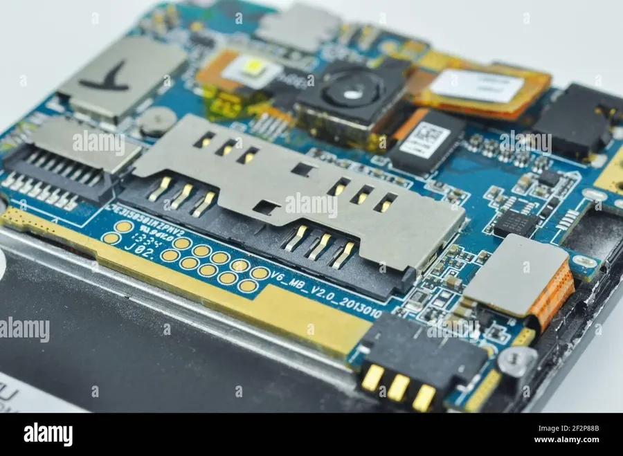
Smartphones, tablets, and laptops rely heavily on PCBs for their complex processing capabilities and interconnectedness. The intricate circuitry of these devices, from the motherboard to the display, is built upon sophisticated PCB designs. - Computing and Data Processing
Desktop computers, servers, and network routers all use PCBs to facilitate data processing and communication. The mainboards, graphic cards, and networking interfaces are all built using PCBs. - Automotive Industry
Modern automobiles feature numerous PCBs for engine control units (ECUs), infotainment systems, advanced driver-assistance systems (ADAS), and safety mechanisms like airbag deployment. PCBs manage crucial vehicle functions and performance. - Medical Equipment
Medical devices, from diagnostic equipment like MRI machines to monitoring devices and implantable technologies, depend on PCBs for their precision and reliability. The accuracy of these tools requires dependable PCB implementations. - Aerospace and Aviation
Aerospace systems require robust PCBs for flight control, navigation, communication, and onboard sensors. Given the harsh operating conditions, PCBs used in this sector need high durability and performance. - Industrial Machinery
Industrial automation, robotics, and control systems all use PCBs for their operation. These systems rely on PCBs for power distribution, motor control, and sensor data processing. - Telecommunications
Communication infrastructure depends on PCBs to support signal transmission and processing across vast networks. From cell towers to data centers, PCBs are the backbone of modern communication.
Frequently Asked Questions About PCB Electronics
This section addresses common questions regarding PCB (Printed Circuit Board) electronics, providing clarity on their purpose, functionality, and cost implications. We aim to enhance your understanding of PCBs through these practical insights.
- What is a PCB and what is it used for in electronics?
A Printed Circuit Board (PCB) is a non-conductive base material, usually fiberglass or composite, with conductive pathways, pads, and other features etched or printed onto it. It is primarily used as a physical support and electrical interconnection platform for electronic components, allowing them to function together as a circuit. Essentially, it's the foundation for almost all electronic devices. - How does a PCB function in an electronic circuit?
PCBs function by providing the physical structure and electrical pathways needed for electronic circuits. The conductive traces etched on the board create specific connections between components, ensuring that signals travel in the designed path. Components are soldered onto the pads, creating a robust and reliable connection. The board itself does not perform computations but facilitates the electrical interaction of the active components. - What are the key differences between PCB types such as single-layer, double-layer, and multilayer?
Single-layer PCBs have conductive traces on one side only and are suitable for basic electronics. Double-layer PCBs have traces on both sides, allowing for more complex circuits. Multilayer PCBs have three or more conductive layers stacked together, offering high density and complexity for advanced electronic devices. The choice depends on the complexity and space requirements of the electronic circuit. - What factors influence the cost of a PCB?
Several factors affect PCB cost, including the type of material used (e.g., FR-4, metal core), the number of layers, board size, the complexity of the design (trace density, number of vias), the finish (e.g., ENIG, HASL), the quantities ordered, and tolerances needed. More complex designs with tighter tolerances and specialty materials will generally increase the price. - Can PCBs be repaired, and what are the implications?
Yes, PCBs can often be repaired, but the feasibility depends on the extent and type of damage. Minor faults like a broken solder joint can be relatively easy to fix, while complex issues like damaged traces or delamination might require specialized equipment and expertise. The repair process involves finding the fault, re-soldering connections, replacing damaged components, and sometimes using specialized chemicals to etch new paths. It's critical to use proper techniques during PCB repair to avoid further damage. - What is the importance of thermal management in PCB design?
Thermal management in PCB design is crucial because electronic components generate heat during operation. This heat needs to be managed effectively to prevent component failure, performance degradation, and reduced lifespan. Poor thermal management can cause overheating and cause components to malfunction. Proper heat dissipation is addressed by using heat sinks, thermal vias, and appropriate layer stack-ups, and thermal-aware component placement. - How does PCB design software aid in the creation of PCBs?
PCB design software, also known as Electronic Design Automation (EDA) software, is essential for designing and creating PCB layouts. It offers tools for schematic capture, layout design, routing, and manufacturing outputs. PCB design software not only automates many aspects of the design process but also ensures accuracy and the ability to perform signal integrity analysis. Without EDA software, the design of complex PCBs would be significantly more time-consuming and prone to error.
The Future of PCB Electronics: Trends and Innovations
The landscape of PCB electronics is rapidly evolving, driven by the increasing demand for smaller, more powerful, and more sustainable devices. This section explores the key trends and innovations that are shaping the future of PCB technology, focusing on high-density interconnects, flexible electronics, and sustainable manufacturing.
- High-Density Interconnects (HDI)
HDI technology focuses on increasing the density of circuitry on a PCB, allowing for more complex and compact designs. This involves using smaller vias, finer traces, and advanced materials to pack more functionality into a smaller area. Key drivers include miniaturization of devices and increased performance requirements. - Flexible Electronics
Flexible PCBs (FPCBs) are gaining prominence, offering the ability to bend, fold, and twist without losing functionality. These PCBs enable the creation of devices that conform to various shapes and surfaces, enabling applications in wearable technology, biomedical devices, and automotive systems. They use flexible substrates and specialized materials to achieve this flexibility. - Sustainable Manufacturing
The electronics industry is increasingly emphasizing environmentally responsible manufacturing practices. This includes the use of eco-friendly materials, reduction of waste, and the development of energy-efficient production processes. Research is ongoing into alternatives to traditional FR-4 materials and less harmful etching chemicals, leading to a greener future for PCB fabrication. - Advanced Materials
New materials with enhanced electrical, mechanical, and thermal properties are being actively developed and adopted. This includes materials with improved signal integrity, better heat dissipation characteristics, and greater flexibility, further enabling the development of high-performance electronics. - Embedded Components
Integrating passive and active components directly into the PCB layers enables miniaturization and reduces the need for surface mount components. This increases circuit density and improves reliability, as well as reduces assembly costs.
Printed Circuit Boards, though often unseen, are the very foundation of our modern technological world. From the simplest single-layer boards to the complex multi-layer designs, PCBs enable the functionality of every device we rely on. A solid understanding of PCB electronics is not just a niche skill but a crucial aspect of the interconnected tech landscape that continues to evolve. Whether you are an electronics enthusiast or just someone curious about what's inside your gadgets, this guide provides a solid foundation to appreciate the importance and ubiquity of PCB electronics in our lives. The continuous innovation in this space promises even more remarkable technological advancements.