Understanding Printed Boards: From Basics to Advanced Applications
In our increasingly interconnected world, the unassuming printed board, or printed circuit board (PCB), is the silent workhorse behind nearly every electronic device we use. From smartphones to spacecraft, these intricate boards provide the essential foundation for electronic circuits. This article will delve into the fundamentals of printed boards, their various types, materials, design, and manufacturing processes, as well as their importance in our everyday lives. Join us as we uncover the core of modern electronics – the printed board.
What is a Printed Board?
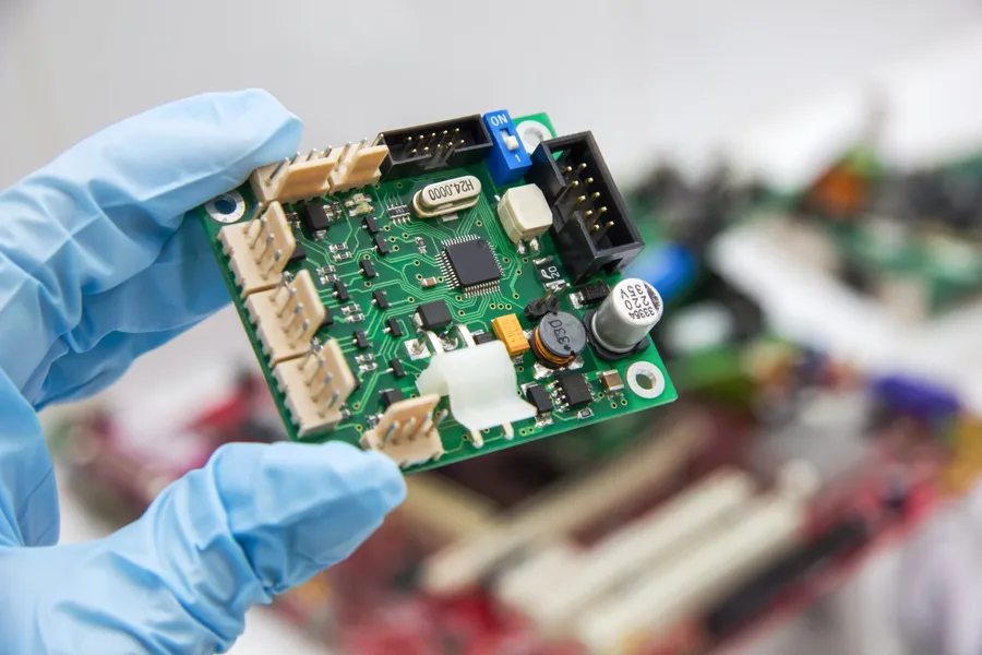
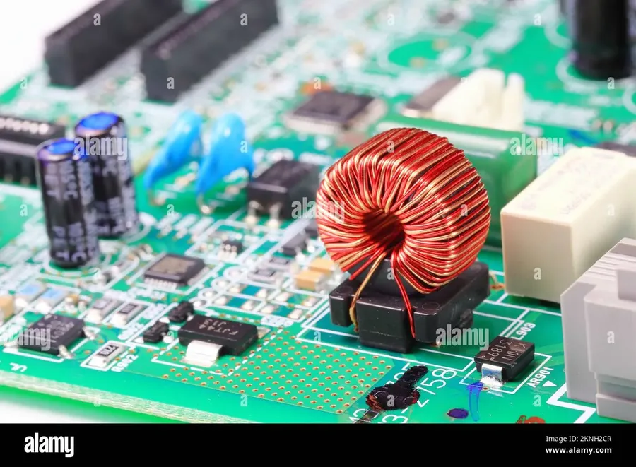
A printed board, commonly referred to as a printed circuit board (PCB), serves as the foundational platform for electronic devices. At its core, a PCB is a non-conductive substrate, typically made of fiberglass or composite epoxy, onto which conductive pathways, or traces, are etched. These traces, usually made of copper, facilitate the electrical connections between electronic components, ensuring the correct function of the overall circuit. The construction and layout of a PCB are critical to a device's performance, reliability, and overall functionality.
Fundamentally, a printed board acts as a mechanical support and electrical connection medium for various electronic components. These components are attached to the PCB's surface using soldering techniques, with their leads or pins connected to the conductive traces. This interconnection network allows for controlled flow of electrical current, enabling the electronic device to perform its intended purpose.
Types of Printed Boards: Rigid, Flex, and Beyond
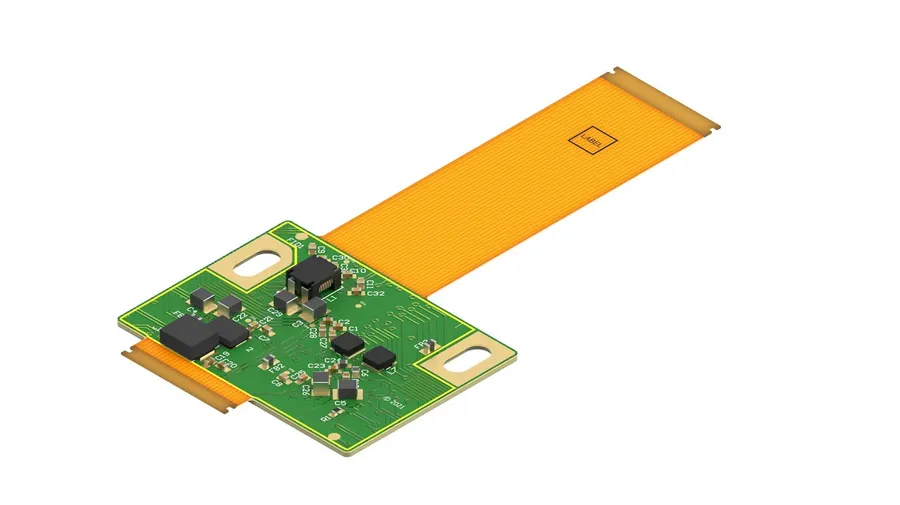
Printed circuit boards (PCBs), or printed boards, are not monolithic in their design and application; rather, they exist in several distinct forms, each tailored to specific functional requirements and environmental conditions. These types range from the ubiquitous rigid PCB to highly specialized flexible and metal-core variants, offering designers a wide spectrum of choices to meet diverse electronic needs.
| PCB Type | Description | Typical Applications | Advantages | Disadvantages |
|---|---|---|---|---|
| Rigid PCBs | The most common type, characterized by their inflexible base material. | Computers, consumer electronics, industrial equipment. | Cost-effective, durable, and widely available. | Limited flexibility, not suitable for dynamic applications. |
| Flexible PCBs | Made with flexible substrate materials, allowing for bending and flexing. | Wearable devices, automotive interiors, medical sensors. | High flexibility, lightweight, and excellent for dynamic applications. | Higher cost, less durable than rigid PCBs, more complex assembly. |
| Rigid-Flex PCBs | Combine both rigid and flexible sections into one board. | Advanced medical devices, aerospace, high-end consumer electronics. | Combines benefits of both rigid and flexible PCBs, saves space, reduced interconnect. | Higher manufacturing cost, complex design and manufacturing. |
| Metal Core PCBs (MCPCBs) | Utilize a metal base material (usually aluminum or copper) to enhance heat dissipation. | LED lighting, power supplies, high-power electronics. | Excellent heat dissipation, enhanced thermal performance, improved reliability. | Heavier, can be more expensive, limited design flexibility. |
| HDI PCBs (High-Density Interconnect) | Characterized by fine lines, small vias, and high component density. | Smartphones, tablets, high-end networking equipment. | Compact size, high density, improved performance. | Higher cost, more complex manufacturing process, requires advanced technology. |
Materials Used in Printed Board Manufacturing
The performance and reliability of a printed circuit board (PCB) are fundamentally linked to the materials used in its construction. These materials, chosen for their specific electrical, thermal, and mechanical properties, directly influence the board's functionality and lifespan. The primary components include the base substrate, conductive materials, and surface finishes, each playing a critical role in the PCB's overall performance.
| Material Type | Material Example | Key Properties | Impact on PCB |
|---|---|---|---|
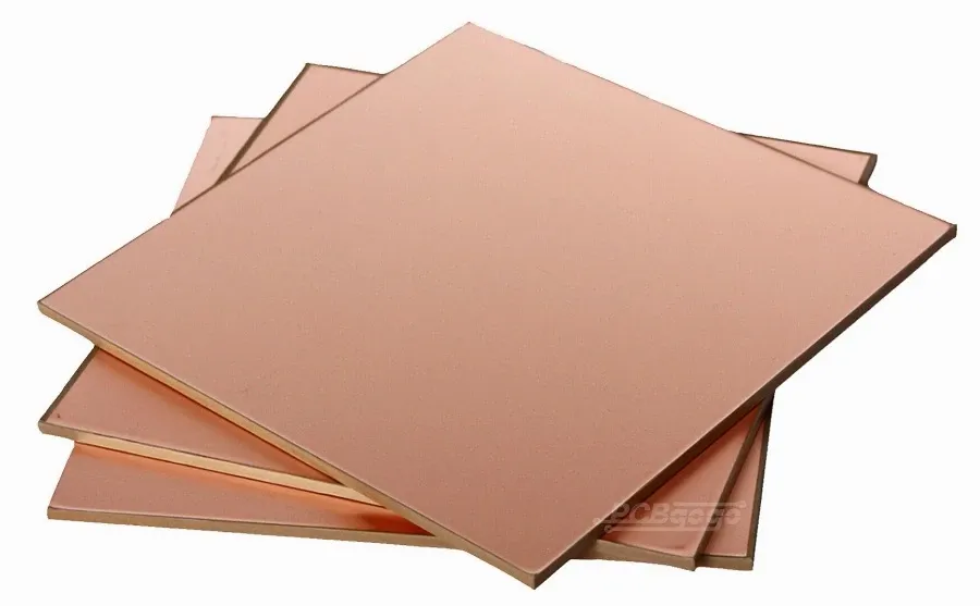
| Base Substrate | FR-4 (Flame Retardant 4) | High strength, good electrical insulation, fire retardant, cost-effective | Forms the structural foundation of the PCB; determines mechanical stability and dielectric properties. |
| Base Substrate | Composite Epoxy | Good dielectric properties, lower cost than FR-4 | Alternative to FR-4; balances cost and performance for less demanding applications. |
| Base Substrate | Polyimide | Excellent temperature resistance, flexibility | Used in flexible PCBs and high-temperature applications. |
| Conductive Material | Copper | High electrical conductivity, good thermal conductivity, malleable | Forms the traces and pads for electrical connections; critical for signal transmission and current flow. |
| Surface Finish | HASL (Hot Air Solder Leveling) | Low cost, good solderability | Protects copper from oxidation; facilitates soldering. |
| Surface Finish | ENIG (Electroless Nickel Immersion Gold) | Excellent solderability and corrosion resistance | Provides a very flat, solderable surface, suitable for fine-pitch components and high reliability applications. |
| Surface Finish | OSP (Organic Solderability Preservative) | Environmentally friendly, good solderability | Offers a thin, protective coating for a short time, good for lead-free assembly |
Printed Board Design Process

The printed board design process is a critical phase in the development of any electronic product, involving the meticulous transformation of an electronic schematic into a physical board layout. This process encompasses several key stages, from initial schematic capture to final routing and verification, emphasizing both functional correctness and manufacturability.
- Schematic Capture
The process begins with translating the circuit's functional requirements into a schematic diagram using Electronic Design Automation (EDA) software. This involves selecting appropriate components from a library and interconnecting them logically based on the intended functionality. Accurate component selection and precise connections are paramount. - Component Placement
Once the schematic is complete, the components are physically positioned onto the virtual printed board layout. Considerations for component placement include signal integrity, thermal management, assembly efficiency, and overall board size. Strategic placement minimizes signal interference, optimizes thermal performance, and facilitates efficient manufacturing. - Layer Stack-up Definition
The number of layers in a PCB, the material used, and the positioning of conductive layers are essential factors that significantly affect the board's electrical and thermal performance. A well-designed stack-up optimizes impedance control and minimizes noise. For instance, multilayer boards may be necessary for complex designs. - Routing
Routing involves connecting the components using conductive traces on the board. This stage requires careful planning to ensure signal integrity, proper impedance matching, and sufficient clearance between traces. Automated routing tools within CAD software assist with this complex task, while human expertise remains critical to ensure optimal outcomes. - Design Rule Checks (DRC)
Before proceeding to manufacturing, the design undergoes thorough checks, ensuring it adheres to predefined design rules and constraints. These checks verify trace widths, clearances, via placement, and other critical aspects to prevent design flaws and facilitate reliable manufacturing. This step is essential to avoid issues during the physical creation of the PCB. - Design For Manufacturing (DFM)
DFM analysis reviews the PCB design from a manufacturability perspective, confirming that the board can be reliably fabricated and assembled. It identifies potential issues that may lead to manufacturing difficulties and suggests design modifications. Incorporating DFM principles ensures that designs are optimized for production efficiency and minimize manufacturing defects. This includes consideration of panelization, fiducial markings, and solder mask clearances. - Output File Generation
After successful DRC and DFM, output files are generated, which typically include Gerber files for the fabrication process, and pick-and-place files for assembly. These files contain all the necessary information for the manufacturer to physically produce the PCB.
Printed Board Manufacturing Process
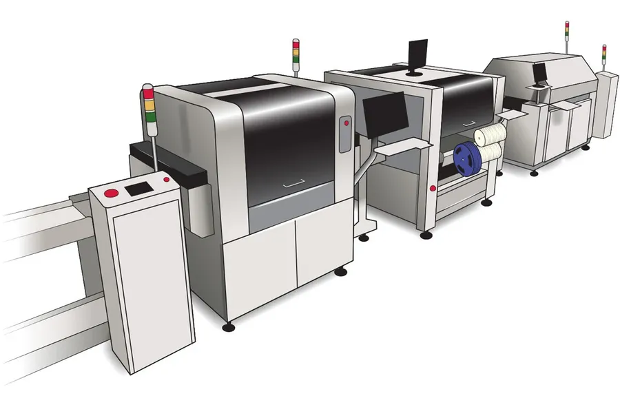
The manufacturing of printed boards, or PCBs, is a complex, multi-stage process involving precise chemical and mechanical techniques. These processes transform raw materials into functional circuit boards, which form the backbone of nearly every electronic device. The process includes steps such as etching, drilling, plating, and soldering.
Below we will explore the typical sequence of operations involved in creating a printed board, the key steps involved and manufacturing method:
- Material Preparation
The process begins with the selection of appropriate base materials, typically including a substrate (such as FR-4), and copper foils. These materials are cut to the desired size and prepared for subsequent stages. - Imaging
The desired circuit pattern is transferred onto the copper surface. This involves applying a photoresist film and exposing it to UV light through a mask containing the circuit layout. The exposed areas of the photoresist harden, while the unexposed areas remain soluble. - Etching
The board is then immersed in an etching solution, which dissolves the copper not protected by the hardened photoresist. This process precisely removes unwanted copper, leaving the desired circuit traces. - Drilling
Holes are drilled through the board using computer-controlled drilling machines. These holes are required for vias (connections between layers) and for mounting electronic components. - Plating
The drilled holes are plated with copper to establish electrical connections between different layers of the board. This is typically done using an electroless plating process followed by electrolytic plating. - Solder Mask Application
A solder mask layer is applied to protect the copper traces from oxidation and prevent solder bridges during component assembly. This mask is also photosensitive and is applied similarly to the photoresist used in the etching process. - Surface Finishing
The board surface is finished with a protective layer, such as gold plating, HASL (Hot Air Solder Leveling), or ENIG (Electroless Nickel Immersion Gold). This finish protects the copper and provides a reliable surface for soldering components. - Silkscreen Printing
A silkscreen is printed on the board surface to provide component designators, logos, and other important information for assembly. - Testing and Quality Control
Finally, the boards undergo electrical testing using automated test equipment (ATE) to ensure the circuit is functional and meets design specifications. Visual inspections are also conducted to ensure quality standards are met. - Cutting & Separation
The finished boards are cut from the larger panel and separated in preparation for assembly
Each of these steps requires meticulous control and adherence to design specifications to ensure the final product meets stringent quality standards. Different manufacturing methods, such as subtractive and additive processes, can be employed depending on the complexity and volume of the printed board.
Applications of Printed Boards Across Industries
Printed boards, or PCBs, are the ubiquitous foundation of modern electronics, enabling the functionality of devices across a diverse spectrum of industries. Their versatility stems from their ability to provide both structural support and electrical connectivity for electronic components, a capability that has propelled innovation in numerous sectors.
- Consumer Electronics
From smartphones and laptops to TVs and gaming consoles, PCBs are the central element. They allow for complex circuit designs in increasingly smaller form factors, enabling the features and performance we expect in these devices. The constant push for miniaturization and increased functionality drives the need for advanced PCB designs and materials. - Automotive
Modern vehicles rely heavily on PCBs for engine control units (ECUs), infotainment systems, safety features like anti-lock braking systems (ABS) and airbags, and advanced driver-assistance systems (ADAS). The automotive industry's demanding environment requires robust PCBs capable of withstanding harsh temperatures, vibrations, and humidity. The transition to electric vehicles further increases PCB demand for battery management systems and power electronics. - Aerospace
In aerospace, PCBs are crucial for flight control systems, communication equipment, navigation systems, and in-flight entertainment. These applications demand high reliability, precision, and resilience against extreme conditions, often necessitating specialized PCB materials and manufacturing processes to meet stringent performance and safety standards. - Medical Devices
Medical devices, including diagnostic equipment, patient monitoring systems, and surgical tools, use PCBs for their accuracy, reliability, and size considerations. The biocompatibility of PCB materials is critical in many medical applications, alongside considerations for low noise and high precision in sensitive medical instrumentation. - Industrial Automation
PCBs are integral to programmable logic controllers (PLCs), robotics, and control systems that drive factory automation. These boards are designed for harsh operating conditions, must be robust, and often require specific certifications related to industrial environments.
Printed Board FAQs: Addressing Common Questions
This section addresses frequently asked questions about printed boards (PCBs), providing clear and concise answers to common queries. These FAQs cover essential aspects of PCBs, from their construction to their applications and impact on electronic products.
- What are the key differences between single-sided, double-sided, and multi-layer PCBs?
Single-sided PCBs have conductive material on one side, limiting their complexity. Double-sided PCBs have conductive layers on both sides, allowing for more intricate routing. Multi-layer PCBs contain three or more conductive layers, separated by insulating material, enabling highly complex and dense circuit designs. The choice depends on the complexity of the circuit, space constraints, and cost considerations. Single-sided PCBs are generally the most cost-effective but have the lowest density, while multi-layer PCBs are more expensive but offer the highest density and performance. - What exactly is PCB assembly, and why is it important?
PCB assembly is the process of mounting electronic components onto a bare printed circuit board (PCB). This includes placing components like resistors, capacitors, integrated circuits (ICs), and connectors onto the board using automated machinery and soldering them into place. PCB assembly is a crucial step as it transforms the bare PCB into a functional electronic circuit or module. Proper assembly ensures reliable electrical connections and correct functionality of the designed circuit. Inadequate assembly can lead to performance degradation or complete system failure. - How are printed circuit boards (PCBs) tested after manufacturing?
PCBs undergo several rigorous testing procedures to ensure their quality and reliability. Common methods include visual inspection to check for defects such as cracks, misaligned components, or solder issues; in-circuit testing (ICT), which uses probes to verify the electrical integrity of the circuits; functional testing, where the board is subjected to typical operating conditions; and automated optical inspection (AOI), using cameras to scan for manufacturing defects. These tests confirm the conformity of the board to the specifications. - Why are printed boards so crucial to the functionality of electronic products?
Printed boards are fundamental to electronic products because they serve as the backbone for electronic circuits, providing a structured platform to support and connect electronic components. They enable electrical signals to flow in a designed manner, are mechanically stable, and provide a means to manage heat dissipation and shielding. Without PCBs, electronic devices would be impractical to manufacture, complex, and unreliable due to the need to wire everything manually. Thus, PCBs are the cornerstone of the electronics industry, ensuring the functionality of devices. - How do material choices affect the performance and cost of printed circuit boards?
The choice of materials significantly impacts both the performance and cost of PCBs. The base substrate material (e.g., FR-4) affects thermal characteristics, mechanical strength, and signal integrity. Conductive material (mostly copper) influences signal transmission efficiency and thermal performance. The surface finish (e.g., ENIG, HASL) affects solderability and corrosion resistance. Higher performance materials (e.g., those with lower dielectric constants) and premium finishes increase the cost but also improve performance and reliability, particularly in high-frequency applications. Balancing material performance requirements and budgetary constraints is vital. - What is the role of copper in printed board manufacturing?
Copper is the primary conductive material used in printed boards due to its excellent electrical conductivity, relatively low cost, and ease of processing. Copper layers are etched into the PCB to form traces and pads that connect electronic components. The thickness and distribution of copper on the board affect current carrying capacity, signal integrity and impedance control.
Future Trends in Printed Board Technology
The printed board industry is experiencing rapid advancements, driven by the ever-increasing demands of modern electronics. These trends are shaping the future of PCB design, manufacturing, and application, moving towards higher performance, greater flexibility, and enhanced sustainability.
- Flexible Electronics Integration
The demand for flexible and wearable electronics is surging, driving the development of flexible PCBs that can bend and twist without compromising functionality. This includes applications in smartwatches, medical sensors, and foldable displays, using materials like polyimide and liquid crystal polymers. - 3D Printed PCBs
Additive manufacturing, or 3D printing, is revolutionizing PCB fabrication, enabling the creation of complex three-dimensional circuit structures within a single step. This eliminates the need for traditional subtractive processes and allows for miniaturized, highly integrated designs. This opens opportunities for more complex circuits and conformal electronics. - Advanced Materials Research
New materials, such as advanced ceramics, graphene, and other nanomaterials, are being explored to enhance the performance of PCBs. These materials offer improved thermal management, higher operating frequencies, and increased mechanical strength, leading to more robust and efficient electronic devices. - Sustainable Manufacturing Practices
Environmental concerns are pushing the industry towards sustainable PCB manufacturing practices. This includes the use of eco-friendly materials, reduced waste generation, and energy-efficient processes. The focus is on creating circular economies within electronics production, with an emphasis on recycling and responsible sourcing. - High-Density Interconnect (HDI) and Advanced Packaging
The demand for smaller and more densely packed circuits has led to the development of HDI PCBs and advanced packaging techniques. These approaches allow for greater component density and improved signal integrity, crucial for high-performance computing and communication systems. These trends are characterized by fine lines and via structures for complex interconnection. - Integration of Artificial Intelligence in PCB Design
AI is being increasingly applied in PCB design, optimizing layouts, signal routing, and performance analysis. AI algorithms can identify potential design flaws, predict performance, and shorten the design cycle, reducing time-to-market for new electronic products. This automation is becoming critical for complex designs.
Printed boards are fundamental to modern electronics, facilitating the seamless operation of countless devices that have become integral to our lives. From simple circuits to complex systems, the design and manufacturing of printed boards are continuously evolving, pushing the boundaries of what’s possible. Understanding the intricacies of printed boards is essential for anyone involved in electronics or technology, and it’s clear that these essential components will only grow in importance as technology advances.