Understanding the Role of the Main PCB in Electronics
In our technology-driven world, the main PCB (Printed Circuit Board) serves as the unsung hero, a foundational component enabling electronic devices to function. Just as the central nervous system is vital for living organisms, the main PCB is the backbone of any electronic system. It's the base where electronic components interconnect, communicating signals and power to bring devices to life. This article will delve deep into understanding the main PCB, its importance, how it works, and its impact on the electronic products we use daily.
What is a Main PCB?
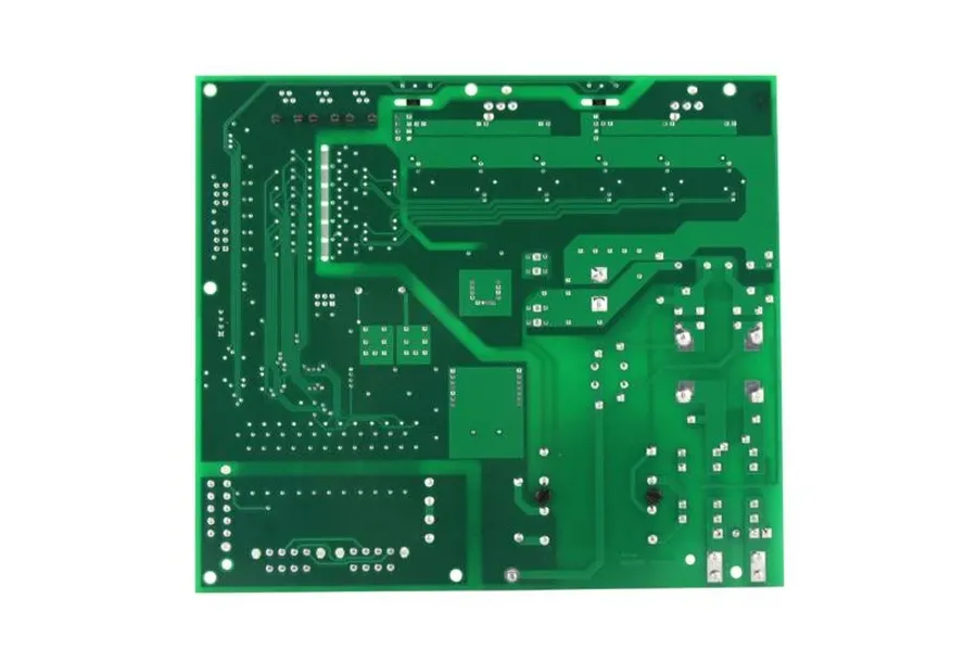
A main Printed Circuit Board (PCB) serves as the foundational platform for electronic devices, functioning as a flat, non-conductive substrate upon which electronic components are mounted and interconnected. This crucial element provides mechanical stability and establishes electrical pathways via conductive traces, typically composed of copper, ensuring the seamless operation of electronic systems.
Key Functions of the Main PCB
The main Printed Circuit Board (PCB) serves as the central functional element within an electronic device, performing several critical roles beyond simple component mounting. It provides the foundational structure for the entire system to operate cohesively and reliably. Its key functions are multifaceted and directly impact the overall performance of the device.
- Mechanical Support
The main PCB provides a rigid, flat platform for mounting and securing electronic components. This ensures that components are precisely positioned and protected from physical stress during operation, handling, and transport. The board's mechanical integrity is essential to maintain reliable interconnections between components. - Electrical Interconnections
The PCB incorporates conductive pathways, typically made of copper, to establish the necessary electrical connections between components. These traces are carefully designed to conduct signals and power efficiently, preventing signal degradation and ensuring proper functionality. The complexity of these interconnections can range from simple point-to-point wiring to intricate multi-layer patterns. - Device Operation
Through its electrical interconnections, the main PCB orchestrates the overall operation of an electronic device. The board’s design and layout play a crucial role in maintaining signal integrity and minimizing noise, which are key factors in ensuring reliable performance. The proper functioning of the circuit is contingent upon a well-designed PCB. - Thermal Management
The PCB acts as a foundation for heat dissipation. Components mounted on the board generate heat during operation, which can affect the components performance and lifespan if not properly managed. The PCB materials and design, including thermal vias and heat sinks, helps regulate temperature distribution and prevent overheating and subsequent failures.
| Function | Description | Impact on Device |
|---|---|---|
| Mechanical Support | Provides a stable platform for components | Ensures components are secure and protected |
| Electrical Interconnections | Establishes conductive pathways for signals and power | Enables communication and functionality between components |
| Device Operation | Orchestrates circuit operation via its interconnections | Ensures signal integrity and proper circuit functioning |
| Thermal Management | Facilitates heat dissipation to prevent overheating | Maintains stable operating temperatures, prolonging lifespan and reliability |
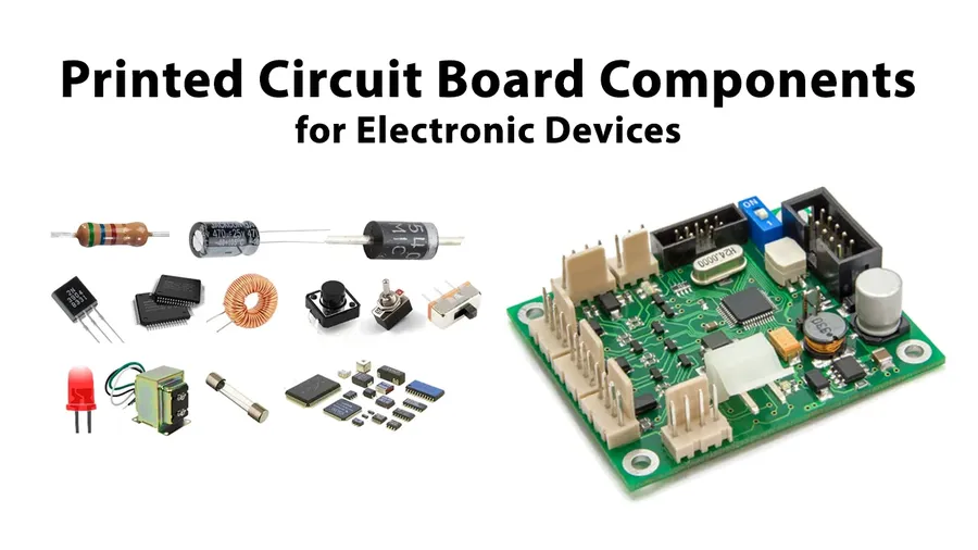
Components Typically Found on a Main PCB
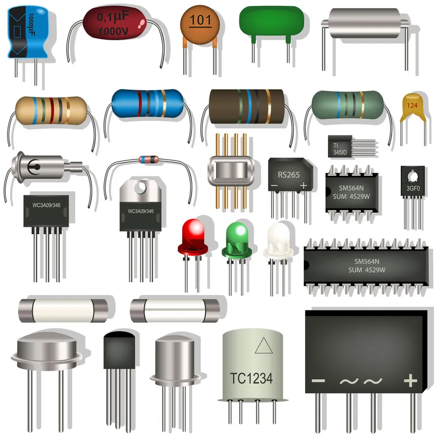
Main PCBs serve as the central hub for electronic devices, hosting a variety of components that work synergistically to achieve the intended functionality. These components range from fundamental circuit elements to complex integrated circuits (ICs), each playing a critical role in the device's operation.
| Component | Function | Description |
|---|---|---|
| Integrated Circuits (ICs) | Processing and logic | Miniaturized electronic circuits that perform specific functions (e.g., microprocessors, memory chips). |
| Resistors | Current control | Limit or resist the flow of electric current. |
| Capacitors | Energy storage and filtering | Store electrical energy and are used for filtering and decoupling. |
| Inductors | Energy storage and filtering | Store energy in a magnetic field and are used in filtering circuits. |
| Connectors | Signal and power interfaces | Provide physical interfaces for signals and power. |
| Diodes | Current direction control | Allow current to flow in one direction only and are used for rectification and signal conditioning. |
| Transistors | Amplification and switching | Used as electronic switches or amplifiers of electrical signals. |
How the Main PCB Impacts Device Performance
The main Printed Circuit Board (PCB) is not merely a passive platform; its design and quality are pivotal determinants of a device's overall performance. Seemingly subtle variations in the PCB's characteristics can manifest as significant differences in signal integrity, thermal management, and ultimately, the device's reliability and longevity.
Several key factors of the main PCB directly influence device performance:
- Trace Width and Spacing:
Trace width dictates the current-carrying capacity of a conductor. Insufficient width can lead to overheating and signal degradation, while excessively wide traces may increase impedance. Spacing between traces affects signal cross-talk and electromagnetic interference. Precisely calculated trace width and spacing are crucial for optimal signal integrity and reducing unwanted noise. - Material Properties:
The dielectric constant and loss tangent of the PCB substrate material significantly impact signal propagation speed and signal losses, respectively. For instance, high-speed digital circuits demand materials with low dielectric loss. Additionally, the thermal conductivity of the material influences heat dissipation from power components. - Component Placement:
The physical placement of electronic components on the PCB can impact thermal distribution and signal path lengths. Strategic positioning of heat-generating components enhances thermal management, while minimizing signal path lengths reduces signal delays and signal reflections. - Layer Stack-up:
The arrangement of conductive and non-conductive layers in a multi-layer PCB significantly influences impedance control, signal integrity, and power distribution. Proper layer stack-up is paramount for complex circuits, such as high-speed digital designs. - Via Design:
Vias are conductive pathways connecting different layers of a PCB, and their design impacts signal integrity and thermal management. Improper via design can cause impedance discontinuities, and increased thermal resistance, affecting overall performance.
For instance, poorly designed traces with insufficient width might cause voltage drops, leading to erratic behavior in digital systems, or overheating in power circuits, causing potential component failure. Likewise, inappropriate choice of PCB materials, for example using a low Tg material for a high-temperature environment, may result in deformation, delamination and failure of the device. Conversely, a well-designed PCB with appropriate trace widths, material choices, and component layout, enables efficient signal transmission, effective thermal dissipation, and reliable device operation.
It's critical to consider not only individual component characteristics but also their interaction within the specific PCB design to achieve optimal and dependable device performance. High-quality PCBs are fundamental to any well functioning electronic system.
Materials Used in Main PCB Fabrication
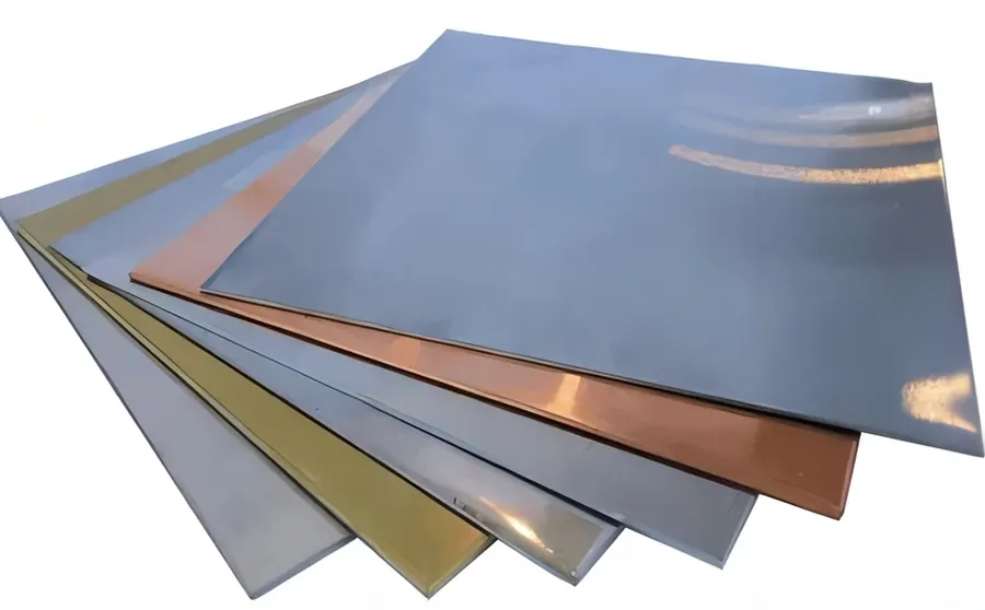
The selection of materials in main PCB fabrication is paramount, directly influencing the performance, cost, and longevity of the final product. The primary materials include the substrate, conductive layers, and protective finishes, each playing a critical role in the PCB's overall functionality and reliability.
| Material | Description | Typical Properties | Application Notes |
|---|---|---|---|
| FR-4 | Fiberglass-reinforced epoxy laminate. | Good mechanical strength, electrical insulation, flame retardant. | Most common substrate material, suitable for a wide range of applications. |
| Copper | Highly conductive metal used for traces and vias. | Excellent electrical conductivity, high thermal conductivity. | Used for signal and power transmission, thickness determines current carrying capacity. |
| Prepreg | Partially cured fiberglass or paper reinforced resin, used as bonding layers. | Acts as an adhesive layer under heat and pressure, providing insulation | Crucial in multi-layer boards, ensures layer to layer adhesion |
| Solder Mask | Resist material which protects copper traces from oxidation. | Provides electrical insulation and protects against shorts, also available in various colors. | Covers the circuit traces and bare vias. |
| ENIG (Electroless Nickel Immersion Gold) | Finish that provides excellent solderability and corrosion resistance | Flat surface, high corrosion resistance, good for wire bonding. | Commonly used for gold plating pads for connections and solder joints |
| HASL (Hot Air Solder Leveling) | Cost-effective tin or tin-lead finish | Good solderability, robust, cost effective. | Covers the copper and solder joints. |
Main PCB Assembly Process
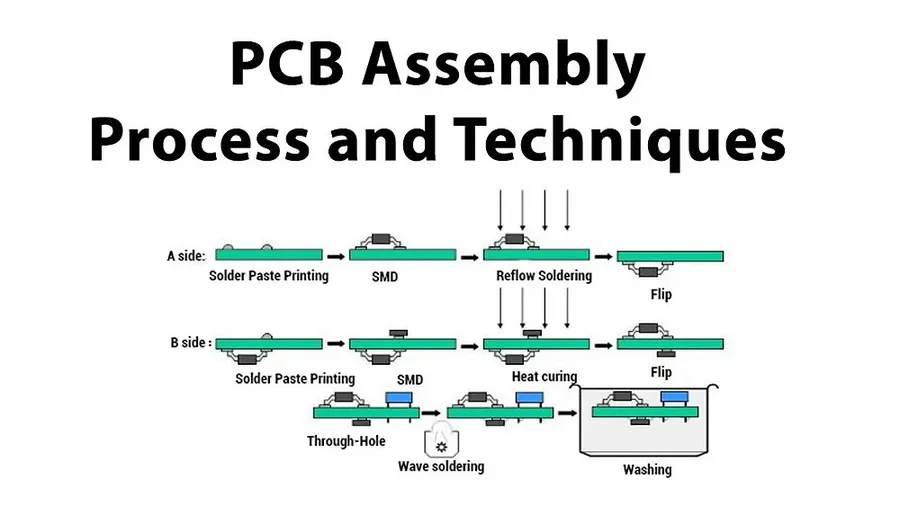
The assembly of a main Printed Circuit Board (PCB) is a complex process involving several critical stages, each demanding precision and adherence to established quality standards. This process converts a bare circuit board into a functional electronic component capable of supporting a wide range of electronic devices.
- PCB Design (CAD/CAM)
The initial step involves translating the circuit's schematic diagram into a physical layout using Computer-Aided Design (CAD) software. This digital representation includes the arrangement of components, traces, and other features. The CAD output is then converted into a Computer-Aided Manufacturing (CAM) file for fabrication. - PCB Fabrication
This stage uses CAM files to manufacture the bare PCB. The process typically involves layering different materials, such as FR-4, etching the copper circuitry, and creating through-holes. The result is a bare PCB ready for component placement. - Component Placement (SMT or Through-hole)
Electronic components are then placed onto the PCB. Surface Mount Technology (SMT) is used for most modern components, where components are placed directly onto the surface of the board. Through-hole technology is used for larger or more robust components, which are placed through pre-drilled holes. Automated machines handle these delicate operations. - Soldering
After component placement, a soldering process permanently attaches the components to the board. This can be accomplished through various methods, including reflow soldering (SMT) or wave soldering (through-hole). Proper soldering ensures reliable electrical connections and mechanical stability. - Testing
Following soldering, the assembled PCB undergoes rigorous testing to verify its electrical functionality. Common tests include in-circuit testing (ICT) and functional testing, checking for continuity, shorts, and correct operation of the circuit. These tests confirm that the board functions according to its specifications. - Quality Control
The final stage encompasses a thorough quality control check. This involves visual inspection for defects such as misalignment, soldering issues, and component damage. PCBs that pass quality control are deemed fit for integration into electronic devices.
Frequently Asked Questions About Main PCBs
This section addresses common questions regarding main Printed Circuit Boards (PCBs), aiming to clarify their purpose, types, and characteristics. Understanding these fundamental aspects is crucial for anyone working with or encountering electronic devices.
- What does PCB stand for in electronics?
PCB stands for Printed Circuit Board. It is a flat, non-conductive board that serves as a base for mounting electronic components. The 'printed' part refers to the conductive pathways, typically made of copper, that are etched onto the board to connect the components. - What is the primary function of a main PCB?
The main PCB’s primary functions are to provide mechanical support for electronic components, offer electrical interconnections between these components, and serve as a foundation for the device's thermal management system, ensuring proper operation and reliability. - What are the key differences between single-layer, double-layer, and multi-layer PCBs?
Single-layer PCBs have conductive pathways on one side only, making them suitable for simple circuits. Double-layer PCBs have conductive pathways on both sides, allowing for more complex designs. Multi-layer PCBs consist of three or more layers of conductive material, enabling very complex and dense circuits suitable for advanced electronics. The choice depends on the application's complexity, cost, and space constraints. - What is the typical material used in main PCB fabrication?
The most common material for PCBs is FR-4, a fiberglass-reinforced epoxy laminate. Copper is used for conductive layers, and various protective finishes, like solder mask and surface plating, are applied to enhance solderability and prevent corrosion. The selection of material impacts performance, cost, and operational longevity of the device. - How does the design of a main PCB influence device performance?
The design of a main PCB directly impacts device performance through factors like trace width, layer stack-up, component placement, and thermal management. Careful layout ensures signal integrity (minimal signal loss and interference), optimized power distribution, and efficient heat dissipation, all crucial for reliable operation. Poor design can lead to performance degradation or failure. - Can a main PCB be repaired if it's damaged?
Yes, minor damages can be repaired through techniques like trace repair, solder reflow, or component replacement. However, the feasibility of repair depends on the extent of damage, the complexity of the PCB, and the availability of specialized equipment and skill. Severe damage might necessitate a complete PCB replacement. - How does a main PCB contribute to thermal management in electronic devices?
Main PCBs facilitate thermal management through design elements such as copper planes, thermal vias and heatsinks. These elements help to dissipate heat generated by electronic components, preventing overheating, which can impact device performance and longevity. Efficient heat dissipation is essential for maintaining optimal operating conditions.
Common Main PCB Failure Points and Troubleshooting
Main PCBs, while crucial for electronic device functionality, are susceptible to various failure modes stemming from manufacturing defects, operational stresses, and environmental factors. Understanding these common failure points and having effective troubleshooting methods is essential for maintaining and repairing electronic systems.
- Faulty Components
Component failures, such as Integrated Circuits (ICs), capacitors, resistors, and transistors, are frequent causes of PCB malfunctions. These can occur due to manufacturing defects, voltage surges, overheating, or aging. Identifying faulty components often requires circuit testing and component-level analysis, with replacements sourced according to the specification to ensure circuit functionality. - Damaged Traces
Copper traces, which act as conductive pathways, can be damaged due to physical stress, corrosion, or excessive heat. Damaged traces disrupt the flow of signals, leading to erratic device behavior or complete system failure. Diagnosis requires visual inspection, and repairs can involve micro-soldering or applying conductive ink to reestablish connections, ensuring proper signal paths are restored. - Poor Soldering Joints
Inadequate soldering, such as cold joints, insufficient solder, or solder bridges, can result in intermittent connections or open circuits. This is often a result of improper manufacturing processes, insufficient heat, and unclean pads during assembly. These issues can be diagnosed using visual inspection, and further inspected using X-ray for hidden defects. Proper soldering techniques, and the implementation of rigorous quality control measures are necessary to address these flaws. - Environmental Exposure
Exposure to moisture, extreme temperatures, or corrosive substances can severely degrade the PCB's performance and reliability. Humidity can cause corrosion and short circuits, while extreme temperatures can lead to material deformation, solder fatigue, and component failures. Implementing preventative measures, including conformal coating, proper storage, and thermal management techniques, are critical to maintain device reliability. - Overheating
Excessive heat generation from components or insufficient thermal management can cause a variety of issues, such as solder joint failures, component degradation, and PCB warping. The heat must be carefully managed to maintain system reliability and longevity. Implementing heat sinks, thermal pads, and optimized airflow paths are critical mitigation methods.
The main PCB is indispensable to modern electronics and its functionality; its design, construction, and maintenance are key aspects of electronics engineering. From the circuit board in your smartphone to the complex boards within industrial machinery, the main PCB serves as the fundamental building block. Understanding its role is essential for appreciating the complexity and precision behind the devices that shape our world. By continually improving PCB technology, we push the boundaries of what's possible in electronics, driving progress across industries.