Unleashing Your Creativity: Exciting PCB Projects for Every Skill Level
In today's world, electronics have become the cornerstone of almost every aspect of our lives, transforming everyday objects with remarkable capabilities. From the phones in our pockets to the smart appliances in our homes, printed circuit boards (PCBs) are the unseen foundation powering these innovations. Whether you are a seasoned maker or just getting started with electronics, engaging with PCB projects can unlock exciting opportunities for learning, innovation, and creation. This article serves as your guide to the world of PCB projects, offering ideas and resources to ignite your curiosity and help you build your own electronic marvels.
Getting Started with PCB Projects: A Beginner's Guide
Embarking on PCB (Printed Circuit Board) projects is an exciting journey into the world of electronics. This section provides a foundational understanding of PCBs, covering essential components, basic circuit concepts, and the crucial steps for building your first successful projects. For beginners, grasping these fundamental principles is key to a fulfilling and educational experience in electronics.
- Understanding the basics of PCBs
PCBs are the foundation of most electronic devices. They provide mechanical support and electrical connections for electronic components through conductive pathways etched onto a non-conductive substrate. Common PCB materials include FR-4 (a fiberglass composite), and understanding their material properties is key. - Essential electronic components
Familiarize yourself with basic components such as resistors, capacitors, diodes, transistors, and integrated circuits (ICs). Understanding their function within a circuit is essential to building projects. A resistor controls current, while capacitors store electrical charge, and diodes allow current to flow in one direction only. - Basic circuit concepts
Learn about basic circuit concepts like voltage, current, resistance, Ohm’s law (V=IR), and series and parallel circuits. These concepts are foundational for designing and troubleshooting simple circuits. Understanding how these parameters interact allows you to predict and control the behavior of a circuit. - Simple circuit concepts
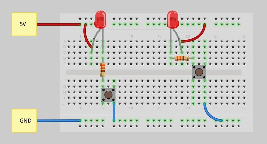
Start with simple circuits to learn the basics of electronic functionality and to understand the role of every component in a circuit, by building simple circuits such as LED blinkers, basic amplifiers, or simple sensor circuits, which will provide hands-on experience and help you gain the skills to move to more complex projects.
Essential Tools and Software for PCB Design
Effective PCB design and fabrication require a suite of specialized tools and software. This section outlines the essential hardware and software components necessary for designing, prototyping, and assembling PCB projects, covering everything from CAD software to soldering equipment.
| Category | Tool/Software | Description | Purpose |
|---|---|---|---|
| PCB Design Software | KiCad | Open-source, cross-platform suite for schematic capture and PCB layout. | Schematic design, PCB layout, generating Gerber files. |
| PCB Design Software | Eagle | Popular PCB design software with both free and paid options. | Schematic design, PCB layout, generating Gerber files. |
| PCB Design Software | Altium Designer | Industry-standard software for complex PCB designs. | Advanced schematic design, high-speed layout, simulation. |
| PCB Design Software | EasyEDA | Web-based PCB design tool, easy to use and suitable for beginners. | Quick PCB design and ordering with integrated LCSC component library. |
| Soldering Equipment | Soldering Iron | Used to melt solder for connecting electronic components. | Assembly of through-hole and surface-mount components. |
| Soldering Equipment | Solder Wire | Alloy with a low melting point used to create electrical connections. | Creating reliable electrical connections. |
| Soldering Equipment | Desoldering Pump/Wick | Used to remove solder from joints for rework or component removal. | Correcting errors and component replacement. |
| Prototyping Equipment | Breadboard | Solderless board for rapid prototyping circuits. | Testing and verifying circuit designs before PCB fabrication. |
| Prototyping Equipment | Multimeter | Electrical measuring device used for voltage, current, and resistance. | Verifying circuit functionality and troubleshooting issues. |
| Prototyping Equipment | Power Supply | Adjustable power source for powering and testing circuits. | Providing controlled power to prototype boards. |
| Component Handling | Tweezers | Small, pointed tools for handling small electronic components. | Placing and manipulating surface mount devices. |
Simple PCB Project Ideas for Beginners
Embarking on your PCB journey is best done with projects that are straightforward yet engaging. For beginners, projects like LED blinkers, basic amplifiers, and simple sensor circuits provide an ideal foundation for understanding circuit design and PCB assembly. These projects not only introduce fundamental concepts but also offer immediate, tangible results, bolstering confidence and encouraging further exploration.
- LED Blinker Circuit
A classic introductory project, the LED blinker uses a 555 timer IC or a microcontroller to periodically turn an LED on and off. This project demonstrates basic timing circuits, power management, and component connection. - Basic Audio Amplifier
Using an operational amplifier (op-amp), this project amplifies a small audio signal. It provides practical experience with analog circuits, signal processing, and gain control, and it is often a stepping stone to more complex audio-related designs. - Simple Temperature Sensor
Implement a simple temperature sensor circuit using a thermistor or a temperature sensor IC. This project introduces the concept of analog input and signal conditioning, as well as the basics of sensor integration into a circuit design. It paves the way to more complex data logging projects. - Light-Activated Switch
A light-activated switch is a basic circuit that uses a phototransistor or a light-dependent resistor (LDR) to control a switch based on the amount of light. This project can be a good introduction to sensor-based circuits, switching circuits and basic control systems.
Intermediate PCB Project Ideas to Expand Your Skills
Moving beyond basic circuits, intermediate PCB projects offer a pathway to deepen your understanding of electronics and embedded systems. These projects typically involve microcontrollers, custom power solutions, and data acquisition, allowing you to integrate more complex functionalities into your designs. This phase is about leveraging your foundation and pushing the boundaries of your skills to build more intricate systems.
- Microcontroller-Based Projects (e.g., Arduino):
Developing circuits around microcontrollers such as Arduino or ESP32 allows for the implementation of complex control systems, automated tasks, and interactive devices. This involves writing code to interface with hardware components. - Custom Power Supply Designs:
Designing your own linear or switching power supply circuits provides essential experience with power electronics. This includes understanding voltage regulation, current limiting, and thermal management. - Data Logging Devices:
Building systems to log sensor data to SD cards or other storage mediums will deepen your understanding of data acquisition and handling. These projects involve interfacing sensors, microcontrollers, and storage devices. - Simple Robotic Systems:
Projects such as a line-following robot or a simple robotic arm provide practical insights into motor control, sensor integration, and basic mechatronics.
Advanced PCB Projects for Experienced Makers
For seasoned makers, advanced PCB projects offer a playground for pushing the boundaries of electronics and engineering. These projects delve into intricate designs and demanding applications, requiring a deep understanding of PCB design principles, component selection, and advanced fabrication techniques. They serve as a platform to apply theoretical knowledge to complex real-world challenges, offering opportunities for significant learning and innovation.
- High-Speed Signal Processing Boards
These boards are designed to handle data at extremely high frequencies, requiring careful attention to impedance matching, trace routing, and signal integrity. They often involve advanced technologies like differential signaling and multilayer PCBs to minimize signal distortion and interference. - Intricate Motor Controllers
Advanced motor controllers go beyond simple on/off switches, implementing sophisticated control algorithms for precise speed, torque, and position control. This can involve designing circuits for field-oriented control, sinusoidal commutation, and sensorless feedback systems. - RF Communication Circuits
These projects focus on designing circuits for wireless communication, such as Bluetooth, Wi-Fi, or custom RF protocols. The design includes impedance-matched transmission lines, filter networks, and antenna designs, which require specific knowledge of radio-frequency engineering. - FPGA-Based Systems
Integrating FPGAs (Field-Programmable Gate Arrays) allows for highly flexible and reconfigurable hardware platforms. Advanced PCB designs for FPGAs need to consider power distribution, high-speed interfaces, and proper thermal management to ensure optimal performance and stability. - High-Precision Sensor Interfaces
Projects involving high-precision sensors, such as pressure, temperature, or inertial measurement units (IMUs), often require low-noise signal conditioning, high-resolution analog-to-digital converters, and precise calibration techniques to maximize data accuracy and reliability.
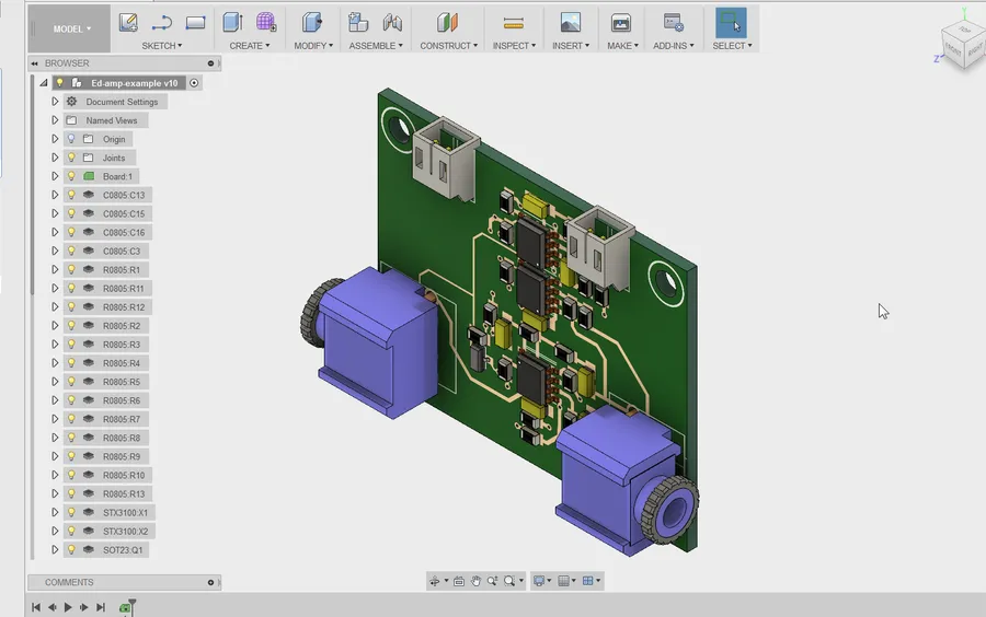
Designing Your Own Custom PCBs: A Step-by-Step Guide
Designing a custom PCB involves a systematic approach, from initial project planning to final fabrication. This process requires a clear understanding of circuit functionality, component selection, and the use of Electronic Design Automation (EDA) tools. This guide provides a structured pathway for creating your own PCBs.
- Define Project Specifications
Begin by clearly defining the function of your PCB. Determine the required inputs, outputs, power requirements, and operating conditions. Create a functional block diagram outlining each stage of your circuit to aid in component selection and layout design. - Schematic Design
Use EDA software to create a schematic diagram of your circuit. This involves selecting appropriate components from libraries, such as resistors, capacitors, integrated circuits, and connectors, and connecting them according to your circuit design. Ensure all component parameters meet the design requirements (e.g., voltage, current, tolerance). - PCB Layout Design
Transfer your schematic to the PCB layout editor within your EDA software. This step involves defining board dimensions, component placement, and routing traces to connect components. Consider factors such as signal integrity, thermal management, and manufacturability. Utilize tools like autorouters judiciously, as manual routing is sometimes necessary for optimal performance. - Component Selection and Footprint Verification
Carefully verify component footprints and ensure they match the selected components. Improper footprints can lead to assembly issues. Check datasheet information for critical dimensions and create custom footprints if necessary. - Gerber File Generation
Once the layout is complete, generate Gerber files using your EDA software. These files contain all necessary information for PCB fabrication, including copper layers, solder mask, silkscreen, and drill holes. Double check the generated files using a Gerber viewer for any errors. - PCB Fabrication
Select a PCB manufacturer. Many online services offer affordable and reliable PCB fabrication. Upload your Gerber files and specify parameters like board thickness, copper weight, and surface finish. Always review the manufacturer's capabilities and requirements prior to uploading files. - Review and Iteration
Carefully review the PCB design for any errors or improvements before submitting for fabrication. It's often wise to have a colleague or mentor review the files as well. Be prepared to make iterative design changes and re-fabricate the PCB as required to get the design perfect.
By adhering to this step-by-step process, you can increase the likelihood of successfully fabricating a functional PCB, while developing a deeper understanding of the underlying engineering principles.
PCB Assembly and Testing: Best Practices
Effective PCB assembly and rigorous testing are crucial steps in ensuring your PCB projects operate as intended. Proper techniques in component placement, soldering, and testing not only prevent functional issues but also contribute to the overall longevity and reliability of your electronic devices.
- Component Placement
Begin by placing larger components first. This allows for easier manipulation and prevents small components from being accidentally dislodged. Use a schematic diagram and a layout plan as guides to ensure correct orientation of each component. Note the polarity of polarized components (diodes, capacitors, LEDs, etc) for correct functionality. - Soldering Techniques
For through-hole components, ensure that the solder joint is smooth and shiny with the right amount of solder. Avoid excessive solder that could create bridges. For surface mount components, use a fine-tipped soldering iron and consider using solder paste. Make sure solder is applied correctly, avoiding any 'cold solder joints' which are a major source of failure. Inadequate heat or too little solder leads to this problem. - Assembly for Through-Hole Components
For through-hole assembly, insert components and then bend their leads slightly to prevent them from falling out during soldering. Use a soldering iron with the right temperature and apply solder to the pad and lead junction to form a strong mechanical and electrical connection. - Assembly for Surface Mount Components
Surface mount assembly can be more delicate. Consider applying solder paste using a stencil, placing the components carefully with tweezers, and then reflowing the solder using hot air. Inspect solder joints with magnification. - Testing methods
After soldering, visual inspection is important, look for solder bridges or faulty solder joints. Use a multimeter to check for shorts and continuity. Power up the board gradually and monitor its current consumption. Check voltages at various points to ensure proper functionality of various circuits. For more complex boards use test points in your design to facilitate troubleshooting.
Frequently Asked Questions About PCB Projects
This section addresses common queries regarding Printed Circuit Board (PCB) projects, offering clear explanations to enhance understanding and confidence in tackling your own designs. It covers essential aspects, from basic concepts to practical implementation, ensuring a comprehensive overview of PCB projects.
- What Exactly Are PCB Projects?
PCB projects involve designing, fabricating, and assembling electronic circuits on a printed circuit board. These projects range from simple LED circuits to complex multi-layered boards for sophisticated electronic devices. They represent the physical manifestation of an electronic design, enabling the interconnection and physical support of electronic components. - What Are Some Common Examples of PCB Projects?
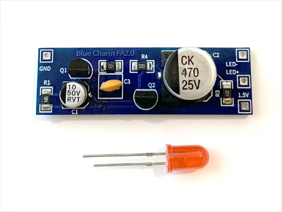
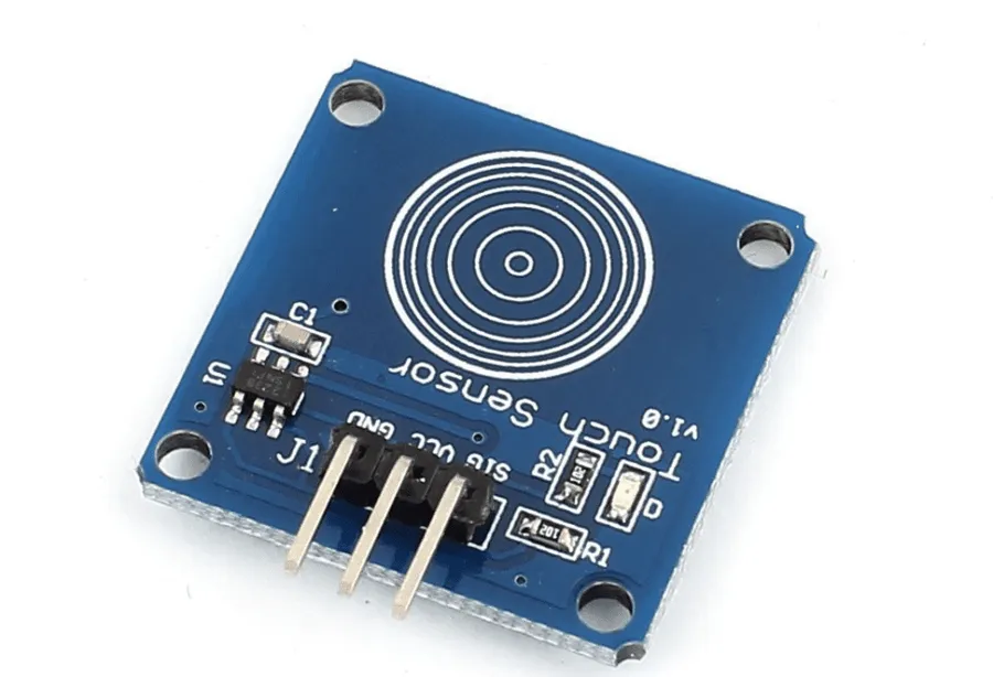
Common PCB projects include LED blinkers, basic amplifiers, power supply circuits, microcontroller-based systems (such as Arduino boards), and various sensor interfaces. More advanced projects encompass high-speed data processing boards, motor controllers, and RF communication circuits. The complexity of these projects varies greatly, suitable for both beginners and experienced makers. - How Do I Start a PCB Project?
Initiating a PCB project involves several steps: conceptualizing your circuit, designing the layout using EDA software, selecting appropriate components, fabricating the PCB through an online manufacturer, assembling the components (soldering), and thoroughly testing the functionality of the circuit. A systematic approach, starting with a clear understanding of the design and objectives, is crucial for success. - What Does PCB Stand For, and Why Are PCBs Important?
PCB stands for Printed Circuit Board. PCBs are critical in modern electronics because they provide a structured and efficient method for connecting electronic components. They eliminate the need for complex point-to-point wiring, which would be impractical for complex circuits, and provide a durable and reliable platform for electronic devices. - What Are the Different Types of PCBs?
PCBs come in various types, including single-layer, double-layer, and multi-layer boards, each with different levels of complexity and capacity. Single-layer PCBs have components on one side, while double-layer PCBs have both sides available for components and traces. Multi-layer boards can have several layers of circuitry, typically used for advanced high-density designs. Additionally, there are flexible PCBs (flex circuits) and rigid-flex PCBs, which combine rigid and flexible materials to provide specific mechanical characteristics. - What Are Some Essential Tools for PCB Project Assembly?
Essential tools for PCB assembly include a soldering iron, solder wire, wire cutters, tweezers, a multimeter for testing, and a desoldering pump or braid for correcting soldering errors. For surface mount technology (SMT) components, hot air stations and magnifying equipment are often necessary. Having the correct tools ensures proper component placement and soldering, leading to reliable and functional circuits. - What Are Some Recommended EDA Software Packages for PCB Design?
Popular EDA (Electronic Design Automation) software packages include KiCad (free and open source), Eagle (Autodesk), Altium Designer, and OrCAD. These tools enable schematic capture, PCB layout design, component library management, and generation of manufacturing files (Gerber files). Choosing EDA software that matches your project requirements and budget is essential for efficient PCB design and fabrication.
Open Source PCB Project Resources and Communities
Open-source platforms and online communities are invaluable resources for PCB project enthusiasts, offering a wealth of designs, collaborative opportunities, and expert support. These resources lower the barrier to entry for beginners and provide advanced makers with sophisticated designs and collaborative environments.
- Open-Source PCB Design Platforms
Platforms such as GitHub, GitLab, and SourceForge host numerous PCB projects, offering access to schematics, layout files, and bill of materials. These resources allow users to inspect, modify, and build upon existing designs, fostering rapid learning and development. - Online PCB Design Communities
Dedicated forums, subreddits (e.g., r/PrintedCircuitBoard, r/electronics), and online maker spaces provide platforms for users to ask questions, share progress, and receive expert feedback on their PCB projects. These communities create an invaluable support network and knowledge base. - Benefits of Open Source
Open-source projects enable rapid prototyping, access to cutting-edge designs, and a collaborative atmosphere where mistakes and successes are shared. This reduces costs and enhances learning curves compared to starting from scratch. - Finding specific projects
Utilize keywords relevant to your project within the search functionality of each resource platform. For example, searching for 'open source motor controller pcb' or 'arduino compatible led driver' can lead to suitable open-source projects for modification.
Engaging in PCB projects offers a unique opportunity to bring your electronic ideas to life. By mastering the design, assembly, and testing processes, you not only gain practical skills but also cultivate creativity and problem-solving abilities. Whether you're a beginner or an advanced maker, exploring these projects can open doors to endless possibilities in the world of electronics, fostering innovation and practical skills, and contribute to an even deeper understanding of the technology around us. Remember to start small, learn continuously, and enjoy the process of bringing your visions to fruition through PCB projects!