Unlocking the Potential of Universal PCB Boards: A Comprehensive Guide
In today's fast-paced world of electronics, prototyping is key to innovation. The universal PCB board, like a blank canvas for your circuits, plays a crucial role in this process. It's the unsung hero of countless projects, from simple DIY creations to complex prototypes. This article will delve into the world of universal PCB boards, exploring their uses, types, and how to leverage them effectively in your next electronics adventure.
What is a Universal PCB Board?
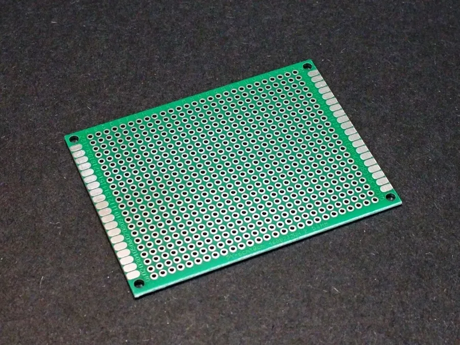
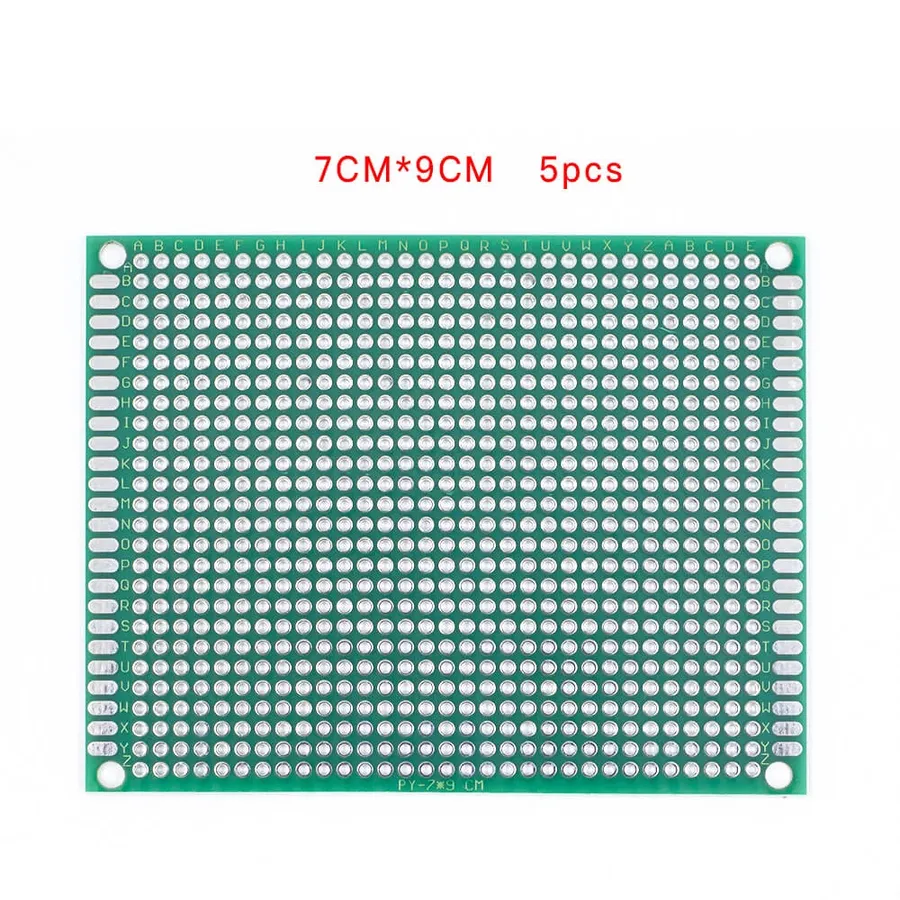
A universal PCB board, often referred to as a proto-board or perfboard, serves as a foundational platform for prototyping electronic circuits. Characterized by a matrix of pre-drilled holes, typically spaced at 0.1 inches (2.54mm), it enables the flexible arrangement and interconnection of electronic components. This design obviates the necessity for custom-designed printed circuit boards, providing an accessible and adaptable means for circuit development.
Types of Universal PCB Boards
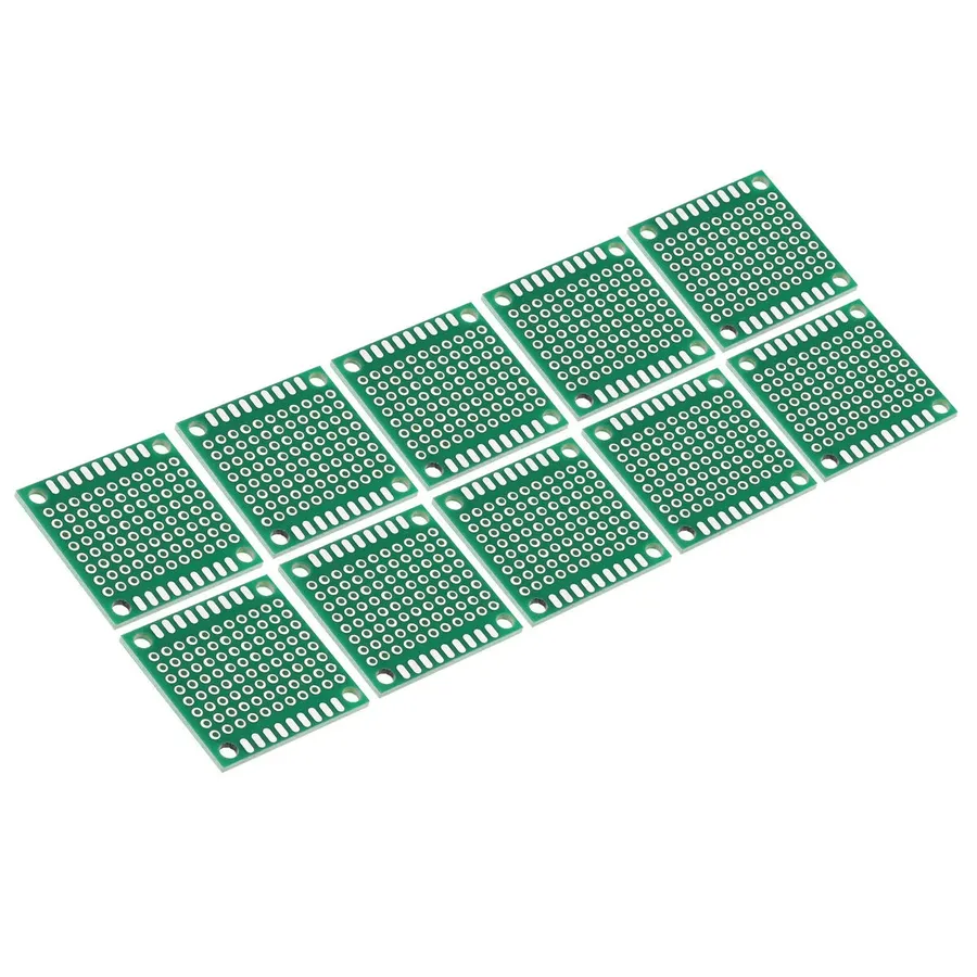
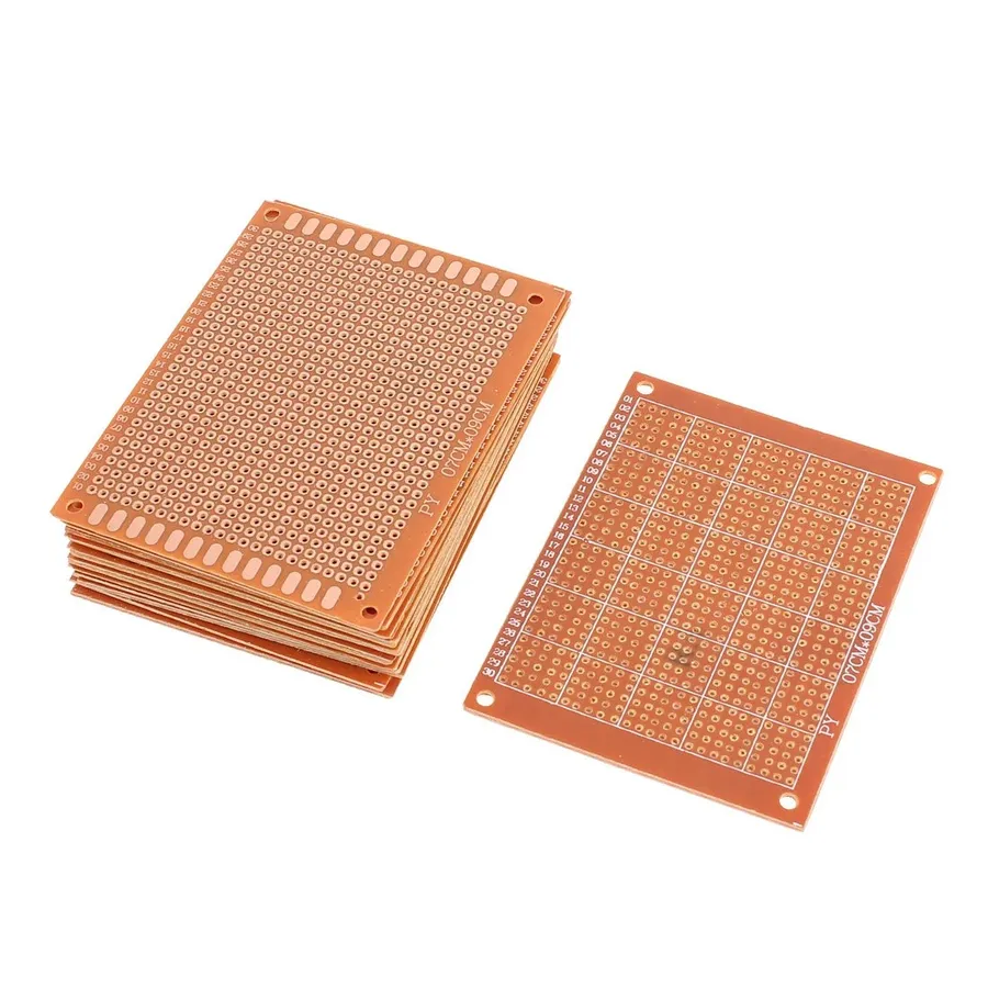
Universal PCB boards, fundamental in electronics prototyping, are available in several variations, primarily distinguished by their copper trace configurations and base materials. These variations cater to diverse project complexities and performance requirements.
| Feature | Single-Sided PCB | Double-Sided PCB |
|---|---|---|
| Copper Traces | Traces on one side only | Traces on both sides |
| Complexity | Suitable for simple circuits | Accommodates more complex circuits |
| Cost | Generally less expensive | Slightly more expensive |
| Use Cases | Basic hobby projects, simple sensor circuits | More complex prototypes, circuits with more components |
The choice of material also significantly influences a PCB’s properties. FR-4 (Flame Retardant 4) is a glass-reinforced epoxy laminate and the most common substrate used due to its excellent balance of electrical insulation, mechanical strength, and thermal stability, including heat resistance. Other materials like phenolic paper boards are available, but they typically have poorer performance and are less durable than FR-4.
Advantages of Using Universal PCB Boards
Universal PCB boards present a compelling array of advantages, particularly in the realm of electronics prototyping and experimentation. Their inherent flexibility and cost-effectiveness make them an invaluable resource for both hobbyists and professional engineers. The key benefits stem from their grid-like structure, which allows for rapid circuit assembly and modification without the need for custom fabrication.
- Rapid Prototyping
Universal PCBs excel in rapid prototyping. Their pre-drilled hole matrix facilitates quick component placement and circuit assembly, allowing for swift testing and iterative design changes. This contrasts sharply with the time-consuming process of custom PCB design and fabrication, making universal boards ideal for preliminary circuit validation and concept exploration. - Cost-Effectiveness
For small-scale projects or one-off builds, universal PCBs are significantly more cost-effective than custom-designed PCBs. The savings arise from the elimination of custom design and fabrication costs, which can be substantial for short production runs. This makes universal boards accessible for educational purposes and for hobbyist projects with limited budgets. - Flexibility in Component Placement
The uniform grid of holes on a universal PCB provides an adaptable platform for arranging various electronic components. This flexibility enables the accommodation of diverse component sizes, shapes, and pin configurations without being confined by specific land patterns. This facilitates the testing and modification of designs with different components and configurations. - Ease of Modification
The design of the board allows components to be easily relocated or changed, making it simple to adapt a circuit. This provides an ease of modification that can be essential when you are exploring different ways to implement the same functionality or when changes are needed based on circuit testing. - Accessibility
Universal PCB's are widely available and easy to procure, making them a convenient choice for many applications. The wide availability of these boards from many different suppliers reduces supply constraints.
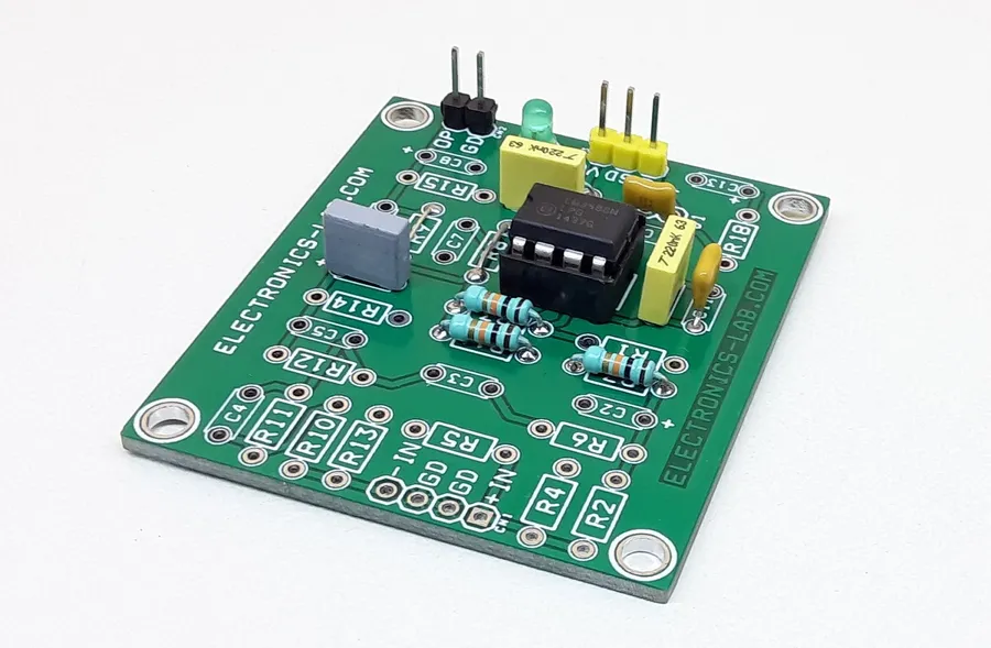
Applications of Universal PCB Boards
Universal PCB boards, characterized by their adaptable nature, serve as a cornerstone in a diverse array of electronic projects. Their flexibility and ease of use make them indispensable tools for various applications, ranging from simple educational exercises to complex system prototyping. They facilitate rapid development and testing, enabling both hobbyists and professionals to efficiently realize their design ideas.
- Hobby Projects
Universal PCBs are widely used by hobbyists to construct various electronic gadgets, circuits, and personal projects. Their ease of use and cost-effectiveness make them ideal for experimentation and learning. - Educational Purposes
In educational settings, these boards provide a hands-on learning platform for students to understand and build electronic circuits. They facilitate practical engagement with theoretical concepts, enhancing the learning experience. - Proof-of-Concept Designs
Before committing to mass production, engineers often use universal PCBs to rapidly test a concept. This approach allows for quick validation of ideas and design modifications as required. - DIY Electronics
DIY electronics enthusiasts rely on universal PCBs to create custom circuits. The ability to freely place components gives them design flexibility to make unique creations and projects. - Sensor Circuit Builds
Universal PCBs are excellent for constructing circuits that interact with various sensors. This includes building environmental monitoring devices, automation systems, or robotics, and provides easy integration with other components. - Initial Testing Phase of Complex Systems
In the development of intricate electronic systems, universal PCBs are useful during the initial testing and prototyping phase. They enable engineers to refine their designs and validate circuit functionality before moving to custom PCBs for mass production.
How to Solder on a Universal PCB Board
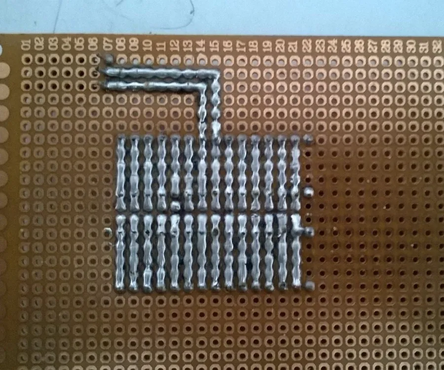
Soldering on a universal PCB board is a fundamental skill for electronics enthusiasts and professionals alike, requiring a methodical approach to ensure reliable electrical connections. The process involves planning the component layout, securing components in place, applying solder to the joints, and diligently checking for errors such as short circuits. Mastering proper soldering techniques, especially heat management and flux application, is crucial for achieving robust and long-lasting connections.
- Planning the Layout
Before beginning to solder, carefully plan the physical placement of components on the universal PCB. Consider the circuit diagram and try to organize the components in a way that minimizes wire crossings and keeps the signal path direct. This planning stage is critical for efficient soldering and a successful final build. - Securing Components
Once your layout is planned, components need to be secured to the board. For through-hole components, insert them into the appropriate holes, and gently bend their leads on the back of the board to hold them in place. This can make soldering much easier and more precise. - Applying Solder
Heat the component lead and the PCB pad simultaneously with the soldering iron. Once both are heated, apply solder to the joint. The solder should flow and form a smooth, cone-shaped joint around the component lead and the pad. Ensure the joint is shiny and not dull, which can indicate a cold solder joint. Use flux to ensure good solder flow. - Checking for Shorts and Errors
After soldering all components, meticulously check for shorts and other errors. A multimeter is essential for this step, allowing you to check for continuity where it should be and for shorts where it shouldn’t. This step is crucial as errors can lead to circuit malfunction or component damage. - Soldering Techniques
Proper heat control is crucial to avoid overheating and damaging components. Apply heat for the minimum time required for the solder to flow. Flux application is also vital; it helps clean the metal surfaces and allows the solder to flow smoothly. Using the appropriate soldering iron tip size for the project is also important.
Choosing the Right Universal PCB Board
Selecting the appropriate universal PCB board is crucial for project success, hinging on a careful evaluation of project needs, which encompasses the board's dimensions, hole spacing, material composition, and complexity of the intended circuit. A well-chosen board will facilitate efficient prototyping and reliable circuit assembly.
| Factor | Considerations |
|---|---|
| Board Size | Match the board size to the scale of your project, ensuring sufficient space for all components. Larger boards provide more flexibility, while smaller boards can be more compact and efficient for simple designs. |
| Hole Spacing | The standard hole spacing is 2.54 mm (0.1 inches). Ensure that this spacing is compatible with the lead pitch of the components you plan to use. Consistent spacing ensures ease of component placement and soldering. |
| Material | FR-4 is the most common material because of its robustness, excellent heat resistance and good electrical insulation. For projects requiring high thermal stability, FR-4 is generally the best choice. Alternatives exist but are less common. |
| Board Type | Single-sided boards are suitable for simple circuits where all connections can be made on one layer. Double-sided boards enable more complex routing and are beneficial when components are on both sides of the board, requiring more space. They allow for greater circuit density and complexity. |
| Component Density | Consider the number of components to be mounted and ensure there's adequate space to prevent overcrowding. Overcrowded boards lead to soldering difficulties and potential connection errors, so plan for ample space. |
| Circuit Complexity | For intricate circuits, double-sided boards are usually necessary to accommodate the additional layers of routing and components. Simple circuits may be constructed on single-sided boards. Choose the board type based on the circuit's overall design complexity. |
Universal PCB Board vs. Custom PCB: When to Choose Which
The selection between a universal PCB board and a custom-designed PCB hinges on project requirements. Universal PCBs are the go-to choice for initial testing, prototyping, and one-off builds due to their flexibility and cost-effectiveness, while custom PCBs become essential for mass production, intricate designs, and when specific performance parameters need to be met. Understanding these differences is paramount in making informed decisions during electronic project development.
| Feature | Universal PCB Board | Custom PCB |
|---|---|---|
| Primary Use | Prototyping, Testing, One-off Projects | Mass Production, Complex Designs, Specific Requirements |
| Cost | Low for small quantities | High for small quantities, lower per unit for mass production |
| Design Flexibility | Flexible component placement, good for simple circuits | Highly specific layouts, optimized for performance |
| Time to Implementation | Quick assembly and modification | Longer lead time required for design and manufacturing |
| Complexity | Suitable for simple to moderately complex circuits | Suitable for multi-layered designs and highly complex circuits |
| Component Density | Lower density due to grid-based layout | Higher density, optimized for the given design |
| Performance | Sufficient for testing and low-speed applications | Optimized for specific performance needs, such as high-frequency circuits |
| Customization | Limited to general layout and component placement | Fully customizable in terms of size, shape, layers, and materials |
Frequently Asked Questions About Universal PCB Boards
This section addresses common questions about universal PCB boards, providing clear and concise answers to help you understand their characteristics, applications, and limitations. We aim to clarify any uncertainties you might have when considering using these versatile prototyping tools.
- What is the primary difference between single-sided and double-sided universal PCB boards?
Single-sided boards have conductive copper traces on only one side, limiting circuit complexity to that single layer. Double-sided boards feature copper traces on both sides, allowing for more intricate and compact circuit designs. This effectively doubles the available area for connections and signal routing, enabling the creation of more complex circuits. Double sided boards can also support vias (vertical interconnect access) allowing for routing of signals between layers. - How durable are universal PCB boards, and what factors affect their lifespan?
The durability of a universal PCB board largely depends on the material used; FR-4 (Flame Retardant 4) is a common and robust choice. Factors such as the number of soldering cycles, physical handling, and environmental conditions like humidity and temperature impact its lifespan. Repeated soldering and excessive mechanical stress can eventually weaken the board. - Can universal PCB boards be used for high-frequency circuits?
While universal PCB boards can be used for prototyping high-frequency circuits, they are not ideal for production due to their inherent limitations. The grid layout and lack of controlled impedance can introduce signal integrity issues, including reflections and signal loss. These boards are best for lower frequency applications or for initial testing of high-frequency designs before migrating to a custom designed PCB with carefully impedance matching. - Is replacing an existing manufactured PCB with a universal PCB board a practical solution?
Replacing a manufactured PCB with a universal PCB is generally not practical for long-term, mass-produced applications. It is more suitable for repairs or replacements where a small batch or one off solution is acceptable. Universal PCB boards lack the precision of custom PCBs, and their performance is usually lower. However, if you need to prototype or develop an alternate fix, they can be useful. - Is it better to use a breadboard or a universal PCB board for prototyping?
Breadboards are excellent for quick, temporary testing because components can be easily added or removed without soldering. However, they are not suitable for permanent designs or when high reliability is needed due to the contact resistances and susceptibility to mechanical disconnect. Universal PCB boards offer a more robust and permanent solution once a circuit design is finalized, and are more suitable for soldered connections. - What is the typical hole spacing on a universal PCB board?
The standard hole spacing on a universal PCB board is 0.1 inches (2.54 mm). This spacing is designed to accommodate a wide range of standard electronic components, such as integrated circuits and discrete parts that often have a 0.1-inch pin spacing. This common spacing allows for ease of prototyping and construction using standard pin headers and connectors. Always check the specification of components for compatibility. - How do you plan the circuit layout on a universal PCB board effectively?
Effective circuit planning on a universal PCB board involves carefully positioning components based on your schematic design and minimizing wire crossings. Use point-to-point wiring, busbars, or other methods to connect components, and always plan your route before soldering. Keep connections short and consider signal paths, while maintaining spacing to avoid overcrowding components.
Tips for Using Universal PCB Boards Effectively
Effective use of universal PCB boards hinges on careful planning and execution. These tips are designed to help you create reliable circuits and avoid common pitfalls.
- Plan Your Layout Ahead
Before placing any components, sketch out your circuit layout. This will help you visualize the connections and optimize the placement of components for minimal wiring and efficient use of space. Consider the signal flow, power distribution, and component proximity. - Use Wire Jumpers for Connections
Employ wire jumpers to establish connections between components. These provide flexibility in routing signals and can be adjusted if necessary, making it easier to modify your circuit. Use different colors for power and signal traces to easily track your connection pathways. - Create Clear and Consistent Layout Designs
Aim for a clear and organized layout. Keep traces straight and use consistent spacing. This not only makes your circuit more visually appealing but also simplifies troubleshooting and maintenance. Uniform layouts prevent signal confusion. - Label Components
Label all components, especially if the circuit is complex. Clear labeling will save time when troubleshooting or modifying the design. This practice helps in easy identification, testing, and prevents errors during assembly. - Avoid Overcrowding Components
Avoid packing components too tightly together. Leaving adequate space between components facilitates easier soldering, prevents short circuits, and assists with heat dissipation. Provide breathing room to maintain proper function. - Always Check Connections Before Powering the Circuit
Before applying power to your assembled circuit, double-check all connections for accuracy and shorts. A thorough pre-power check is vital to prevent damage to components and ensure proper functionality. - Test the Circuit After Assembly
After assembly, thoroughly test your circuit using appropriate testing instruments to ensure all components work as expected and the circuit is performing according to your design parameters. Incremental testing is advisable for complex systems.
Universal PCB boards are an indispensable tool for electronics enthusiasts and professionals alike. Their versatility and ease of use make them perfect for prototyping and experimenting. Whether you're building a simple sensor circuit or a more complex electronic device, understanding how to leverage the power of a universal pcb board will significantly enhance your electronics development journey. They remain crucial in today's innovative landscape, serving as the fundamental stepping stone from concept to functional reality.