Unveiling the Power of HDI PCB: A Comprehensive Guide
In today's fast-paced technological landscape, the demand for smaller, faster, and more efficient electronics is ever-growing. This has led to the rise of High-Density Interconnect (HDI) PCBs, a sophisticated technology that packs more functionality into less space. HDI PCBs aren't just a marvel of engineering; they're a crucial enabler of the cutting-edge devices we rely on daily, from smartphones to medical equipment. This article dives deep into what makes HDI PCBs unique and how they are transforming the electronics industry.
Understanding HDI PCB Technology
High-Density Interconnect (HDI) PCB technology represents a significant advancement in printed circuit board manufacturing, characterized by its ability to pack more functionality into a smaller area. This is achieved through higher wiring density, finer lines and spaces, and the implementation of advanced via technologies, enabling the creation of compact, high-performance electronic devices.
Key Features of HDI PCBs
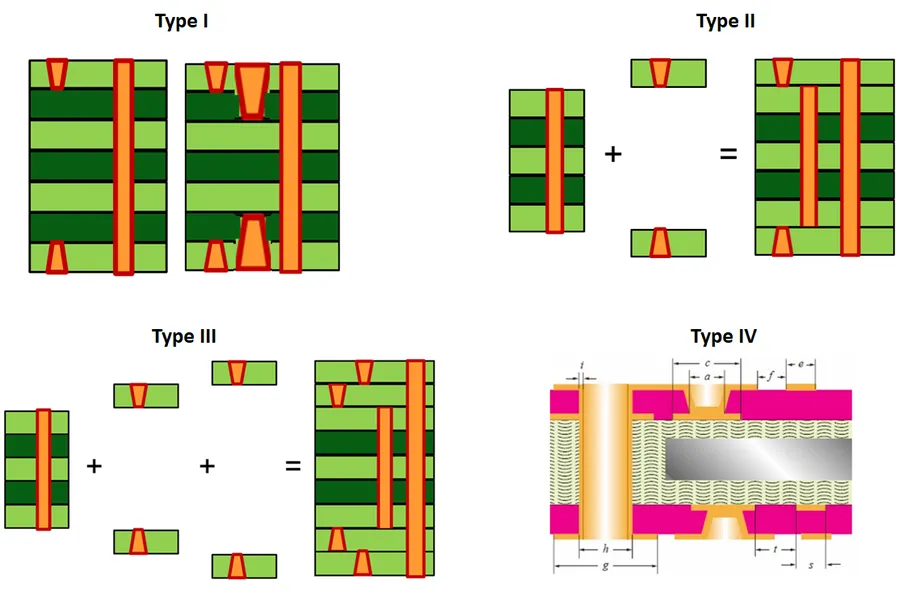
High Density Interconnect (HDI) PCBs achieve their superior performance through several key features centered around advanced via technologies. These features facilitate increased wiring density and miniaturization of electronic devices, offering enhanced electrical performance and design flexibility.
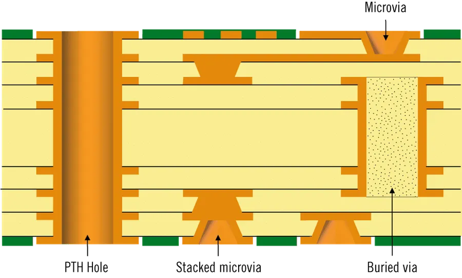
- Microvias
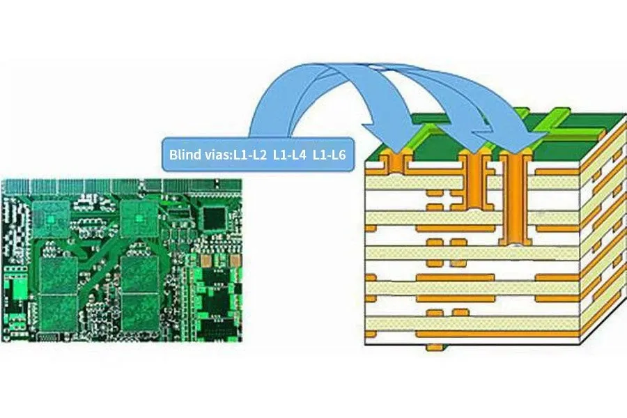
Microvias are extremely small vias, typically with diameters of 150 microns or less, created using laser drilling. They connect adjacent layers, enabling very dense routing and contributing significantly to the miniaturization of HDI PCBs. Their precise nature and minimal size allow for higher interconnection density. - Blind Vias
Blind vias connect an outer layer to one or more inner layers, without passing through the entire PCB. This allows for layer-specific connections and helps maintain signal integrity by reducing stub lengths which can cause signal reflections. - Buried Vias
Buried vias connect two or more inner layers of the PCB without connecting to the outer layers. These vias are completely internal and enable the creation of complex internal routing networks without interfering with surface layer components. - Via-in-Pad
Via-in-pad technology involves placing vias directly within the surface mount pad area of a component. This significantly increases routing density as it enables vias to be incorporated within the component footprint. It is a critical feature in very high-density applications, although it demands precise manufacturing control.
The Advantages of Using HDI PCBs
High-Density Interconnect (HDI) PCBs offer a multitude of advantages over traditional PCBs, primarily stemming from their ability to achieve higher wiring densities, and improved electrical performance. These advantages translate to smaller, more efficient, and more versatile electronic devices.
- Size Reduction
HDI PCBs enable significant miniaturization of electronic devices. By using microvias and finer line traces, HDI technology allows for more components and functionalities to be packed onto a smaller board. This is particularly crucial for portable electronics where size is a critical factor. - Improved Electrical Performance
The shorter and more densely packed traces in HDI PCBs lead to reduced signal path lengths, which minimizes signal reflections and propagation delays, resulting in improved signal integrity and faster data transfer rates. This is especially important for high-speed and high-frequency applications. - Enhanced Signal Integrity
HDI PCBs maintain signal integrity through reduced parasitic capacitance and inductance due to shorter traces and tighter spacing. This leads to cleaner, more stable signals with minimal signal loss, critical for accurate data transmission and reliable performance. - Increased Design Flexibility
HDI technology allows for more complex and intricate circuit designs, providing greater flexibility for layout. With the use of blind and buried vias, components can be placed on multiple layers, optimizing the use of board real estate and enabling more compact and functional designs. This flexibility is crucial for meeting the diverse needs of modern electronics. - Thermal Management Improvements
The increased layer count and use of vias in HDI PCBs improve thermal performance compared to traditional boards. The vias act as thermal pathways, allowing heat to dissipate more effectively, leading to greater stability and reliability.
When compared with traditional PCBs, HDI PCBs are essential for advanced electronic designs. Traditional PCBs, while suitable for many standard applications, cannot achieve the fine features and high density needed for modern electronics. This makes HDI PCBs the only option for smaller, high performance devices.
Common Applications of HDI PCBs
High-Density Interconnect (HDI) PCBs are indispensable in modern electronics, enabling the miniaturization and performance enhancements demanded by today's sophisticated devices. Their unique capabilities allow for complex circuit designs within remarkably compact footprints, making them the technology of choice for applications where space is at a premium and performance is critical.
- Smartphones and Mobile Devices
The miniaturization trend in smartphones necessitates HDI PCBs for complex logic boards, integrating features such as high-resolution displays, multiple camera systems, and advanced connectivity (5G, Wi-Fi, Bluetooth) into compact form factors. - Wearable Technology
Smartwatches, fitness trackers, and other wearable devices utilize HDI PCBs to pack significant computing power and sensing capabilities into incredibly small and lightweight packages, often requiring flexible or rigid-flex circuit boards. - Medical Devices
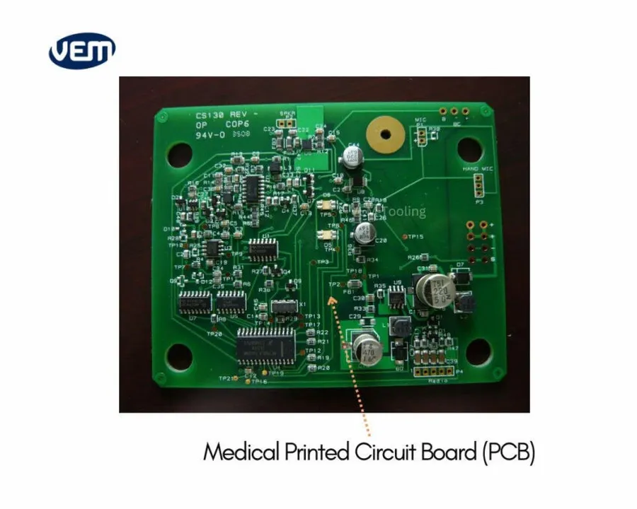
Medical applications, such as diagnostic equipment, portable monitoring devices, and implantable technologies, leverage HDI PCBs for their high reliability and performance, often adhering to strict regulatory standards for accuracy and patient safety. - Automotive Electronics
Automotive systems, including advanced driver-assistance systems (ADAS), infotainment systems, and engine control units, benefit from the robustness and efficiency of HDI PCBs, which must withstand extreme operating conditions and high-vibration environments. - Aerospace and Defense
The rigorous requirements of aerospace and defense applications, including avionics systems, satellite electronics, and communication equipment, rely on the superior performance and reliability offered by HDI PCBs, which often must function under extreme temperatures, pressures, and vibrations. - High Performance Computing
HDI PCBs are employed in high performance computing applications, such as servers, networking equipment and data centers. The increased density allows for faster data transfer speeds and more efficient thermal management.
HDI PCB Design Considerations
Effective HDI PCB design necessitates a meticulous approach, considering factors such as material selection, layer stack-up, and routing strategies. These considerations directly influence the performance, reliability, and manufacturability of the final product. A thorough understanding of these aspects is essential for successful HDI PCB implementation.
- Material Selection
Choosing the right material is critical for HDI PCBs. Key factors include the dielectric constant (Dk), dissipation factor (Df), thermal conductivity, and coefficient of thermal expansion (CTE). Materials like modified epoxy resins, high-performance laminates, and ceramic substrates are frequently used for HDI applications. Selecting materials with appropriate electrical and mechanical characteristics ensures optimal signal integrity and reliability. The choice of material often depends on the operational environment and performance requirements. - Layer Stack-Up Design
Layer stack-up is a critical aspect of HDI PCB design. It dictates the signal integrity, power distribution, and overall performance of the board. A well-designed layer stack-up involves strategic placement of signal, power, and ground layers to control impedance, minimize crosstalk, and provide adequate power distribution. Common stack-up configurations include microstrip and stripline designs. The choice of stack-up also affects the complexity and cost of manufacturing. - Routing Strategies
HDI PCBs require sophisticated routing techniques to accommodate the high density of components and interconnections. Fine-line routing, impedance control, and via management are crucial aspects. Techniques such as differential pair routing, impedance matching, and length matching are essential for maintaining signal integrity. Advanced routing tools and techniques are used to optimize the layout and minimize signal reflections and distortions. Efficient routing also contributes to minimizing manufacturing costs. - Microvia Design
The effective design and implementation of microvias are paramount for HDI PCBs. Considerations include microvia size, location, aspect ratio, and via fill material. Microvias should be designed to minimize impedance discontinuity and ensure reliable electrical connections. The size and density of microvias are limited by manufacturing capabilities, making precision design crucial. - Thermal Management
HDI PCBs often operate in thermally demanding environments. Hence, effective thermal management is crucial. Design techniques such as the use of thermal vias, heat sinks, and thermally conductive materials help dissipate heat. The design should be optimized to ensure that the temperature of critical components remains within acceptable limits, promoting long-term reliability. Careful thermal analysis is a vital step in the design process.
Manufacturing Processes for HDI PCBs
The fabrication of High Density Interconnect (HDI) PCBs necessitates specialized manufacturing techniques to achieve their characteristic high wiring density and miniaturized features. These processes deviate significantly from those used in traditional PCB manufacturing, requiring greater precision and control.
Key manufacturing processes for HDI PCBs include:
- Laser Drilling
Microvias, which are essential for HDI's high density, are created using laser drilling. Precise laser beams, typically UV lasers, ablate the dielectric material to form very small holes (typically less than 150μm) that are then metallized to form electrical connections between layers. This method is preferred over mechanical drilling due to its accuracy and ability to create smaller vias. - Sequential Lamination
HDI boards often require multiple layers of circuits and interconnections. Sequential lamination involves adding layers of copper and dielectric materials step-by-step with each new layer incorporating specific circuit patterns or vias. This method is more complex than traditional single lamination, but allows for higher layer counts and denser interconnects within the PCB. - Fine Line Etching
HDI circuits necessitate fine lines and spacing. Advanced etching techniques are required to create these minute features accurately with very tight tolerances. These may include modified wet etching or semi-additive processes involving photoresist and electroplating to define circuit patterns. - Microvia Metallization
After drilling, the microvias must be metallized to create electrical pathways between layers. This usually involves a combination of electroless plating and electrolytic plating, where thin layers of copper are deposited within the microvias to form reliable and conductive interconnects. - Via Filling
To prevent solder from wicking into vias and potentially causing issues, vias are often filled with conductive or non-conductive materials. The filling process is particularly crucial for via-in-pad designs and is often done using specialized equipment and processes.
The precision and control of these processes are extremely critical as minor errors can lead to functionality issues in the finished product. Proper material selection and process parameter optimization are crucial for reliable and consistent HDI PCB manufacturing.
HDI PCB vs. Traditional PCB: A Comparison
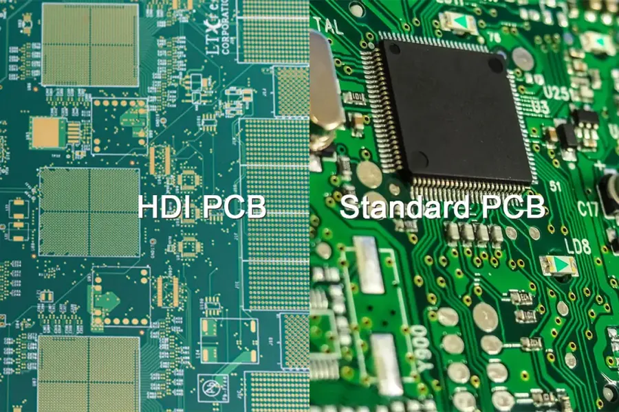
High-Density Interconnect (HDI) PCBs represent a significant advancement over traditional PCBs, primarily distinguished by their enhanced wiring density, use of advanced via technologies, and increased circuit complexity. This section provides a detailed comparison between HDI and traditional PCBs, highlighting their key differences in terms of design, performance, cost, and suitability for various applications.
| Feature | HDI PCB | Traditional PCB |
|---|---|---|
| Wiring Density | High; finer lines and spaces, microvias | Lower; larger lines and spaces, through-hole vias |
| Via Technology | Microvias, blind vias, buried vias, via-in-pad | Through-hole vias |
| Layer Count | Potentially higher; capable of complex multi-layer designs | Typically lower; simpler layer structure |
| Size and Weight | Smaller and lighter for the same functionality | Larger and heavier for equivalent functionality |
| Design Complexity | Higher; requires advanced design tools and techniques | Lower; simpler design requirements |
| Signal Integrity | Superior; shorter signal paths, reduced signal reflection | Lower; longer signal paths, more susceptible to signal issues |
| Cost | Higher; due to specialized manufacturing processes and higher yields. | Lower; simpler manufacturing processes |
| Application Suitability | Ideal for compact, high-performance devices such as smartphones, wearables, medical devices, aerospace and advanced automotive applications | Suitable for simpler, less demanding applications, and devices where space and size are not critical factors. |
Frequently Asked Questions About HDI PCBs
This section addresses frequently asked questions about High-Density Interconnect (HDI) PCBs, providing clear and concise answers to common queries regarding their design, manufacturing, and application.
- What is the fundamental difference between HDI and non-HDI PCBs?
HDI PCBs are characterized by higher wiring density per unit area, achieved through finer lines and spaces, microvias, and advanced via technologies. Non-HDI PCBs, conversely, have lower wiring densities and use larger features. This density disparity allows HDI PCBs to pack more functionality into a smaller footprint, whereas non-HDI PCBs require larger physical dimensions to achieve similar functionality. - What are the performance limitations of HDI PCBs?
While HDI PCBs offer significant benefits, they can present challenges related to signal integrity due to their higher densities and finer traces which increase the likelihood of cross-talk and impedance mismatches. They also exhibit manufacturing constraints because of their complex design that demands precise and repeatable processes, and increased thermal sensitivity given that the density may lead to higher power dissipation in smaller area. - What is the prevailing IPC standard for HDI PCBs?
The primary standard for HDI PCBs is IPC-2226, which provides guidelines for HDI PCB design including stack-up, via technology, and trace and space requirements. IPC-6012 also relevant provides performance specifications and acceptance criteria for rigid printed boards, including HDI PCBs. These standards specify the design, fabrication, and performance requirements for HDI PCBs ensuring quality and reliability. - How does the cost of HDI PCBs compare with traditional PCBs?
HDI PCBs generally incur a higher cost compared to traditional PCBs. This is due to the sophisticated manufacturing processes needed, such as laser drilling, sequential lamination, and fine-line etching, as well as the use of more expensive materials like resin-coated copper (RCC). Although the initial investment is higher, the reduced size, improved performance, and design flexibility can make HDI PCBs more cost-effective for certain applications over the life cycle. - What are common material options for HDI PCB fabrication?
The material selection for HDI PCBs is vital for its performance, common materials include high-performance resin systems such as those based on epoxy, polyimide, and advanced composite materials. These materials should exhibit excellent dielectric properties, high thermal resistance, and low coefficient of thermal expansion. Resin-coated copper (RCC) is a key material in HDI PCB fabrication. Material selection is determined by the application requirements, operating temperatures, and reliability requirements of the finished product. - What are the advantages of using microvias in HDI PCBs?
Microvias, typically created by laser drilling with diameters ≤ 150 µm, significantly increase the routing density in HDI PCBs. Microvias allow for more efficient layer-to-layer connections, enabling complex designs in a smaller form factor, and also reduce signal reflections. Their small size and density enhance signal integrity by shortening trace lengths and minimizing impedance mismatches. - Can the design of HDI PCB be fully automated and what challenges are involved?
HDI PCB design can be highly automated using CAD/CAM software capable of handling complex routing and via placement. However, challenges remain in fully automating the design because the very fine dimensions and intricate layers necessitate careful considerations that cannot always be implemented by software alone. Design for manufacturability (DFM) and design for testability (DFT) analysis are still required which requires engineering expertise and cannot be completely automated.
HDI PCB technology is at the forefront of modern electronics, enabling the miniaturization and enhanced performance of many of our daily devices. From the complex microvias to the increased wiring density, HDI PCBs represent a significant leap in printed circuit board technology. As we move towards more integrated and compact electronics, understanding and utilizing HDI PCB technology will become even more crucial for product innovation and advancement. Its capacity to integrate more functionality into smaller spaces makes it an indispensable tool for future electronic design.