Unveiling the Power of PCB Power Amplifiers: Design, Types, and Applications
In our interconnected world, the ability to amplify signals is crucial, and PCB power amplifiers stand at the forefront of this technology. From driving your favorite tunes to powering critical industrial equipment, these tiny but powerful circuits are indispensable. This article delves into the inner workings of PCB power amplifiers, explores their diverse applications, and guides you through the key aspects of their design and implementation. Prepare to uncover the secrets behind this fundamental component of modern electronics.
What is a PCB Power Amplifier?
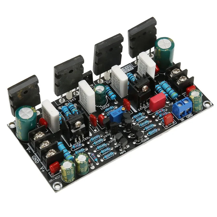
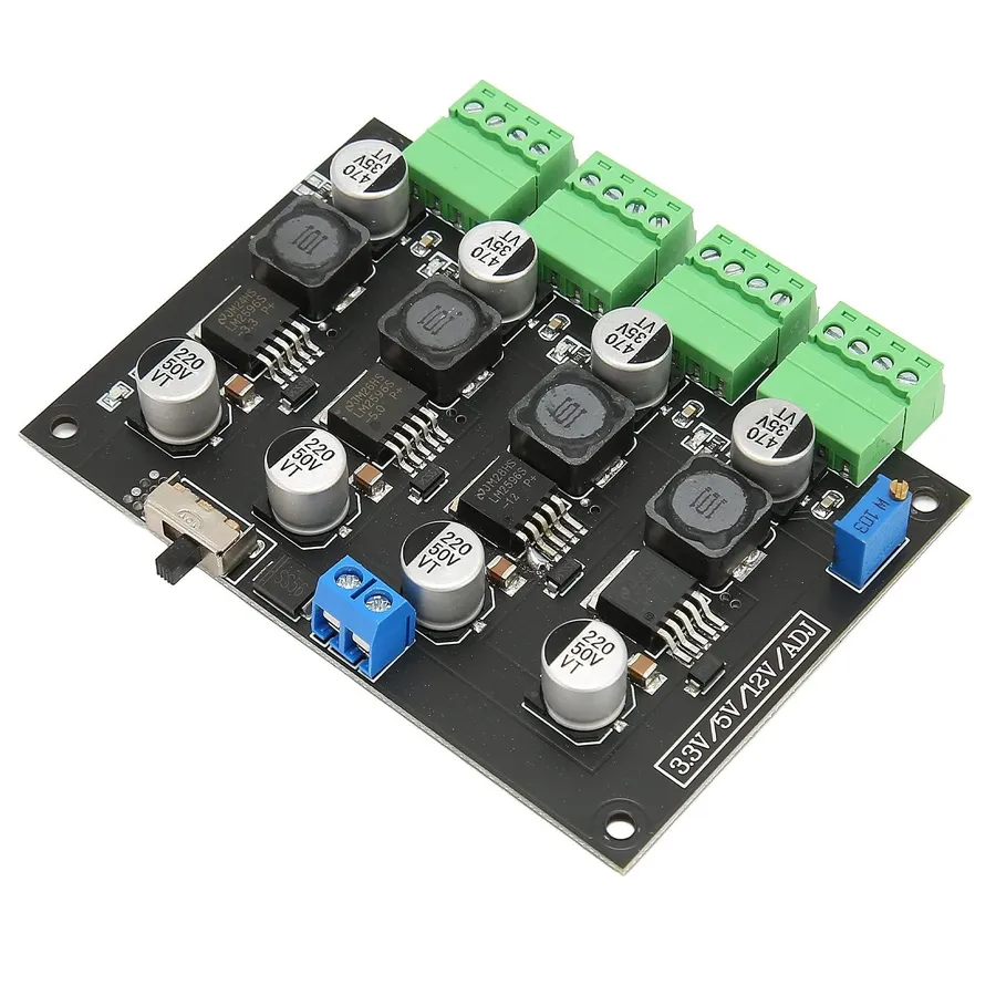
A PCB power amplifier is a specialized electronic circuit, constructed on a printed circuit board (PCB), designed to boost the power of an electrical signal. This amplification is crucial in a wide array of applications, from driving audio speakers and transmitting radio waves to more complex tasks requiring a significantly enhanced signal strength. Fundamentally, it takes a weak input signal and outputs a stronger, amplified version of that signal, ensuring it has sufficient power to perform its desired function.
Key Components of a PCB Power Amplifier
The functionality of a PCB power amplifier is determined by the strategic integration of various electronic components. These components work collaboratively to amplify electrical signals, and their selection and arrangement are paramount to the overall performance of the amplifier. The core components include transistors, operational amplifiers, capacitors, resistors, and inductors.
| Component | Description | Function in Power Amplifier |
|---|---|---|
| Transistors (BJT or MOSFET) | Semiconductor devices used to switch or amplify electronic signals and power. | Primary active device for amplification; controls current flow to boost signal power. BJTs are current-controlled and MOSFETs are voltage-controlled switches. |
| Operational Amplifiers (Op-Amps) | High-gain electronic voltage amplifiers with differential inputs and a single-ended output. | Used in pre-amplification stages to provide voltage gain and drive the main power transistors; can also be used in feedback loops to improve stability and reduce distortion. |
| Capacitors | Passive two-terminal electronic components that store energy in an electric field. | Used for filtering, decoupling, and energy storage; block DC and allow AC signals to pass, often used to smooth out the power supply and stabilize the amplifier's operation. |
| Resistors | Passive two-terminal electronic components that oppose the flow of electric current. | Used to set gain, bias operating points, limit current, and provide a stable operating environment for the amplifier; critical for setting transistor operating parameters and shaping the frequency response. |
| Inductors | Passive two-terminal electronic components that store energy in a magnetic field. | Used for impedance matching, filtering, and forming resonant circuits; often employed in output stages to filter harmonics and ensure stable operation across the desired frequency range. |
Classes of Power Amplifiers: A, B, AB, C, D and Beyond
Power amplifiers are categorized into classes, each with unique operating characteristics that affect efficiency, linearity, and suitability for different applications. These classes, primarily A, B, AB, C, and D (along with other variations), represent distinct approaches to amplifying electrical signals, each with associated trade-offs.
| Class | Conduction Angle | Efficiency | Linearity | Typical Applications |
|---|---|---|---|---|
| A | 360° | Low (max 25%) | High | High-fidelity audio, low-power applications |
| B | 180° | Medium (max 78.5%) | Low (significant distortion) | Push-pull circuits, not used in high fidelity applications |
| AB | Between 180° and 360° | Medium (25-78.5%) | Moderate | Audio amplifiers, general-purpose amplifiers |
| C | Less than 180° | High (up to 90%) | Low | RF signal amplification, oscillators |
| D | Switching | High (up to 90% or more) | High, through use of PWM | Audio amplifiers, motor controls, power supplies |
| G/H | Varying, based on signal | Medium to High | Good | High-efficiency audio amplifiers |
Class A amplifiers conduct throughout the entire input cycle, resulting in high linearity but low efficiency. Class B amplifiers only conduct during half of the input cycle, increasing efficiency but creating significant distortion. Class AB amplifiers are a compromise, offering better efficiency than Class A and lower distortion than Class B. Class C amplifiers have the highest efficiency but the lowest linearity, making them suitable for RF applications. Class D amplifiers use switching technology which gives them high efficiency but requires careful filtering.
Understanding the conduction angle, which is the portion of the input cycle when the active device conducts current, is key to grasping the operational differences. This angle dictates linearity and efficiency trade-offs. Classes G and H are variations which dynamically adjust the power supply voltage based on input, boosting efficiency further.
PCB Design Considerations for Power Amplifiers
Designing a Printed Circuit Board (PCB) for power amplifiers requires meticulous attention to detail, going beyond basic circuit layout to ensure optimal performance, reliability, and longevity. Effective PCB design for power amplifiers involves managing thermal dissipation, ensuring signal integrity, and mitigating noise, thereby demanding a multi-faceted approach.
| Design Consideration | Description | Importance |
|---|---|---|
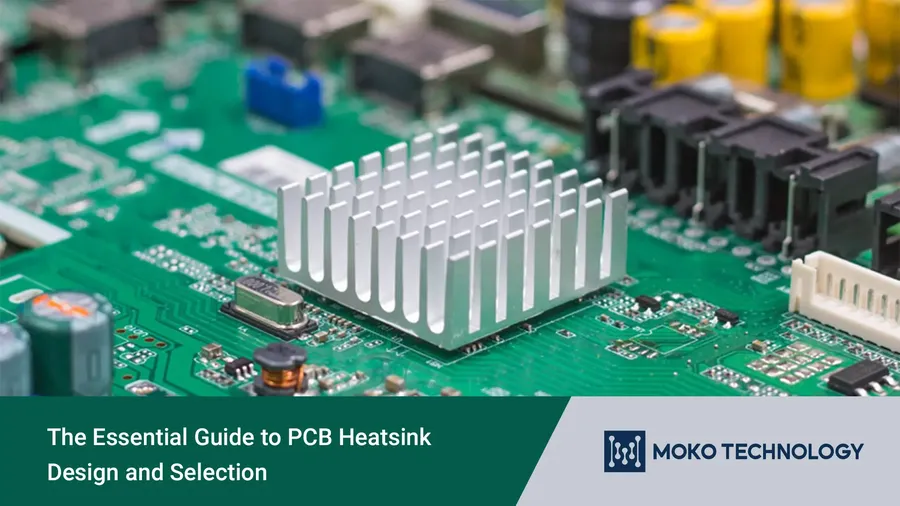
| Thermal Management | Implementing thermal vias, heatsinks, and optimizing component placement for heat dissipation. | Prevents overheating, ensures component reliability and stable operation. |
| Component Placement | Strategic arrangement of components to minimize signal path lengths and reduce parasitic effects. | Improves signal integrity and reduces electromagnetic interference (EMI). |
| Trace Routing | Careful design of PCB traces to maintain impedance control, reduce signal reflections, and ensure proper current handling capabilities. | Preserves signal fidelity, minimizes signal loss, and avoids current-induced damage. |
| Power Plane Design | Employing dedicated power planes to provide a low-impedance path for power distribution and improve noise performance. | Reduces power supply noise, improves overall amplifier stability and performance. |
| Grounding Techniques | Using proper grounding strategies (e.g., star grounding, ground planes) to minimize ground loops and noise. | Reduces ground noise, improves stability and reduces signal distortion. |
Failing to address these PCB design considerations can lead to several issues, including reduced efficiency, signal distortion, component damage from excessive heat, and overall instability of the amplifier circuit. A holistic design approach that includes all of the above is therefore essential for constructing a functional and reliable PCB power amplifier.
Power Supply Design for PCB Amplifiers
A stable and clean power supply is paramount for achieving optimal performance from PCB amplifiers. The power supply directly influences the amplifier's output fidelity, efficiency, and overall reliability. Noise, instability, or inadequate current delivery from the power supply can result in distortion, reduced output power, and even damage to the amplifier components.
The design of a suitable power supply for a PCB amplifier requires careful consideration of several factors, including the amplifier's current requirements, voltage stability, and acceptable noise levels. Both linear and switching power supplies are common choices, each having its advantages and disadvantages depending on the application.
| Characteristic | Linear Power Supply | Switching Power Supply |
|---|---|---|
| Efficiency | Lower (typically 30-60%) | Higher (typically 70-95%) |
| Noise | Lower output noise and ripple | Higher switching noise, requires filtering |
| Cost | Generally simpler and less expensive for low power applications | Generally more complex and expensive but can be cost-effective for higher power applications |
| Complexity | Simpler design, fewer components | More complex design, more components (e.g. inductors, capacitors, switching ICs) |
| Size and Weight | Larger, heavier due to transformer and heat sinks | Smaller, lighter due to high-frequency operation |
| Regulation | Good voltage regulation | Good voltage regulation when designed correctly, potential for overshoot/undershoot |
| Heat Dissipation | Significant heat dissipation due to linear operation | Less heat dissipation at higher efficiency but switching can cause localized heating |
| Typical Applications | Low-noise audio applications, sensitive analog circuits | Portable devices, high-power applications, and systems requiring efficient power conversion |
Proper filtering and regulation are vital in mitigating power supply noise. Filtering typically involves the use of capacitors and inductors to smooth out variations and reduce unwanted high-frequency components. Regulation ensures that the voltage delivered to the amplifier remains stable, even under changing load conditions.
Applications of PCB Power Amplifiers
PCB power amplifiers are integral to a multitude of electronic systems, serving as the crucial link in enhancing signal strength for diverse applications. Their versatility stems from their ability to be tailored to specific power and frequency requirements, making them essential in both consumer and industrial electronics.
- Audio Amplification
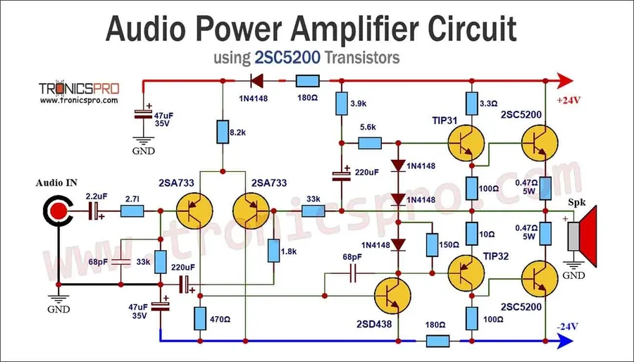
In audio applications, PCB power amplifiers drive speakers in various systems, from home theater setups and car audio systems to headphones and portable audio devices. These amplifiers provide the necessary power to convert weak audio signals into sound waves strong enough to be heard, thus impacting the clarity, loudness, and quality of the audio output. They often require high fidelity, low distortion, and precise control over the frequency response, so Class AB amplifiers are commonly used in this scenario. - RF Power Amplification
RF (Radio Frequency) power amplifiers on PCBs are crucial for transmitting wireless signals. They are used in wireless communication systems (cellular, Wi-Fi, Bluetooth), radar systems, medical devices that employ RF energy, and various scientific instrumentation. These amplifiers must operate efficiently at high frequencies, often requiring specialized designs and components to handle the high power levels and heat dissipation. Classes C, D, E, and F are common depending on the specific application. - Industrial Applications
In industrial settings, PCB power amplifiers are used for motor control and power inverters. They can amplify control signals to drive large motors with precision, as well as convert DC power into AC power for various industrial applications. This category often uses high power levels and requires robust, reliable amplifiers that can withstand harsh industrial environments. These applications often utilize class D amplifiers. - Specific Examples
Beyond the broad categories, there are many niche applications for PCB power amplifiers such as in the control systems of unmanned aerial vehicles (UAVs), instrumentation amplifiers for scientific sensors, and medical equipment that needs precise signal amplification. Each application has unique requirements in terms of power, frequency response, efficiency, size, and overall performance. This emphasizes the need to customize amplifier design based on specific end-user needs.
DIY PCB Power Amplifier Projects
Embarking on a DIY PCB power amplifier project offers an engaging way to understand electronics principles and create customized audio solutions. This section guides you through the necessary steps, components, and considerations for building a functional amplifier, tailored for both beginners and intermediate enthusiasts.
Successful DIY projects hinge on careful planning and execution. Here's a breakdown of key steps:
- Project Planning and Schematic Selection
Begin by selecting a suitable amplifier schematic based on your experience level and desired performance. Several readily available schematics online, ranging from simple single-transistor amplifiers to more complex op-amp designs, can be found. Consider the gain, frequency response, and power output requirements. - Component Acquisition
Procure all the necessary components such as transistors (BJT or MOSFET), op-amps, resistors, capacitors, inductors, and potentiometers. Ensure that the components' ratings meet or exceed the design specifications. Always source components from reputable distributors to ensure quality and authenticity. - PCB Design and Fabrication
Transfer the chosen schematic to a PCB layout. Several PCB design software packages are available, including free versions, which can aid in layout optimization. Pay close attention to signal and power trace routing, component placement for optimal thermal management, and grounding techniques. If you choose to fabricate the PCB yourself, you'll need copper clad boards, etchant, and drilling tools; otherwise, a reliable PCB manufacturer can be selected. - Component Assembly
Solder the components onto the PCB with precision, ensuring no shorts or cold solder joints. Refer to the component datasheet for correct orientation. Start with smaller, simpler components before moving to larger, more complex ones. Use a good quality soldering iron and solder for a professional finish. - Power Supply Integration
Connect a stable and appropriate power supply to the PCB amplifier. Always use a well-regulated power supply to prevent noise and component damage. Double-check the polarity before energizing the circuit. If required build a dedicated PSU for the project. - Testing and Calibration
After assembly, conduct initial tests using a signal generator and oscilloscope to verify the amplifier's performance. Check for gain, frequency response, and any distortions. Calibrate the potentiometers (if present) for optimal output. For audio amplifier testing a suitable audio signal source and speaker could be used. - Enclosure and Finishing
Once the amplifier is fully tested and functioning correctly, mount the PCB assembly in an appropriate enclosure to protect the circuitry and provide necessary heat sinking.
Tools and techniques you'll need include:
- Soldering Iron and Solder
A temperature-controlled soldering station is recommended. - Multimeter
Essential for voltage, current, and resistance measurements. - Oscilloscope
Helpful for visualizing waveforms and measuring signal characteristics (e.g., frequency, amplitude). - Signal Generator
Necessary for testing the amplifier with specific input signals. - PCB design software and/or PCB manufacturing partner
For creating a suitable PCB layout and having it fabricated. - Assorted Hand Tools
Including wire strippers, cutters, and tweezers. - Safety equipment
Including safety goggles and a fume extractor, or working in well ventilated location.
By following these steps, both beginners and intermediate users can create their own functional PCB power amplifiers, gaining valuable hands-on experience in electronics design and fabrication.
Frequently Asked Questions About PCB Power Amplifiers
This section addresses common inquiries regarding PCB power amplifiers, offering clear and concise answers to enhance understanding and assist in practical application.
- What exactly is a PCB power amplifier?
A PCB power amplifier is an electronic circuit fabricated on a printed circuit board (PCB) designed to increase the power of an input electrical signal. It serves to enhance the amplitude of the signal, allowing it to drive loads like speakers or transmitting antennas more effectively. The 'power' aspect refers to the ability to deliver substantial current and voltage, not just signal gain. - What are the primary classes of power amplifiers and how do they differ?
Power amplifiers are broadly categorized into classes (A, B, AB, C, D, etc.) each with unique characteristics. Class A amplifiers offer high linearity but low efficiency, suitable for high-fidelity audio. Class B amplifiers improve efficiency but introduce crossover distortion. Class AB is a compromise, offering decent linearity and efficiency. Class C amplifiers are highly efficient but very non-linear, ideal for radio frequency applications. Class D amplifiers achieve high efficiency through pulse-width modulation (PWM) but require filtering. The choice of class depends on the application's specific needs for efficiency, linearity, and power output. - What distinguishes a power amplifier from a regular amplifier?
While both amplifiers increase signal strength, a power amplifier is specifically designed to deliver significant power to a load (e.g., a speaker or antenna). A standard amplifier, like an operational amplifier (op-amp), is typically designed to provide voltage gain with minimal current output, suited for processing signals at lower power levels. Power amplifiers are optimized for current delivery, thermal management, and impedance matching to effectively drive a connected load. Therefore, the primary distinction lies in their output power and intended application—power amplification versus signal conditioning. - What role does the PCB power supply play in the performance of an amplifier?
The power supply is paramount for a PCB amplifier's stable and efficient operation. It provides the necessary DC voltage and current to power the amplifier's active components. A stable, low-noise power supply minimizes distortion and ensures the amplifier's output signal is clear and accurate. Noise from the power supply can manifest as unwanted artifacts in the output signal. Therefore, proper filtering, regulation, and decoupling are vital to maintain signal integrity and optimal amplifier performance. Poor power supply design will result in poor performance even with a perfectly designed amplifier circuit. - How does heat management impact PCB power amplifier design?
Heat management is crucial in PCB power amplifier design due to the generation of heat from power dissipation. Inadequate heat management can lead to thermal runaway, component damage, or reduced amplifier performance. Design strategies include heat sinks, thermal vias, and proper component placement to enhance heat dissipation. Consideration of materials with good thermal conductivity, and forced air or liquid cooling may be required for high power designs. Careful attention to thermal design is necessary to ensure long term reliability and performance of the amplifier. - What are the key PCB layout considerations for a power amplifier circuit?
Key layout considerations include trace width for power delivery, component placement to minimize signal path lengths, and the use of ground planes to reduce noise and impedance. Impedance matching between stages of the amplifier, as well as between the amplifier and the load, is vital to maximizing power transfer and stability. Avoiding sharp bends in traces and employing star or multiple grounding points can minimize noise and improve signal integrity. The use of decoupling capacitors near power pins is also important. Careful layout design is critical for optimal amplifier performance and robustness.
Troubleshooting Common Issues with PCB Power Amplifiers
Effective troubleshooting of PCB power amplifiers requires a systematic approach to diagnose and rectify common issues such as signal distortion, overheating, and signal degradation. By identifying the root cause and methodically applying corrective actions, optimal performance can be restored.
- Distortion
Distortion in the output signal often indicates a problem in the amplifier's bias circuitry or an overloaded input signal. Begin by inspecting the bias voltages against the amplifier's datasheet specifications. If the bias is within spec, evaluate if the input signal exceeds the amplifier's rated input range. Overdriving the input can create non-linear behavior and distort the signal. - Overheating
Excessive heat generation is usually a sign of inefficient amplifier operation or inadequate thermal management. Check the amplifier's quiescent current (current draw when there's no input signal) which should be within datasheet limits. If the current draw is excessive, this usually indicates a problem with the amplifier's active components. Inspect all thermal connections including heatsinks and thermal vias, ensuring these are correctly installed and in good contact. - Signal Degradation
Signal degradation often points to issues within the amplifier's signal path, power supply or grounding. Evaluate impedance matching using an appropriate signal analyzer, high impedance mismatching can degrade the signal. Inspect the power supply, making sure it provides stable, low noise and the required voltage to the amplifier. Improper grounding, including ground loops can cause noise and signal degradation. Review the PCB grounding system for flaws. - Oscillation
Unwanted oscillation can be caused by feedback through the PCB or an unstable power supply. Check for any layout problems that could be causing parasitic feedback. This can also be the result of an inadequate decoupling capacitor. - Component Failure
Component failure within the amplifier can lead to many problems, such as a no signal output. Inspect all active components and passive components for signs of physical damage or overheating. If any component looks damaged, replace it with a compatible component.
PCB power amplifiers are the workhorses of modern electronics, providing the necessary signal boost for myriad applications. Whether you are a seasoned engineer or an aspiring hobbyist, understanding their intricacies is essential for designing robust and high-performing systems. The continued advancements in materials and design techniques ensure that the field of PCB power amplifiers will remain innovative and indispensable for years to come. The future of PCB power amplifiers lies in further improving their efficiency, miniaturization, and performance for our increasingly technological world. From enhancing home entertainment to advancing communications, PCB power amplifiers continue to shape the way we experience the world around us.